EP0342940B1 - Vorrichtung und Verfahren zur Kühlung von Substraten - Google Patents
Vorrichtung und Verfahren zur Kühlung von Substraten Download PDFInfo
- Publication number
- EP0342940B1 EP0342940B1 EP89304958A EP89304958A EP0342940B1 EP 0342940 B1 EP0342940 B1 EP 0342940B1 EP 89304958 A EP89304958 A EP 89304958A EP 89304958 A EP89304958 A EP 89304958A EP 0342940 B1 EP0342940 B1 EP 0342940B1
- Authority
- EP
- European Patent Office
- Prior art keywords
- article
- seat
- substrate
- gas
- cooling
- Prior art date
- Legal status (The legal status is an assumption and is not a legal conclusion. Google has not performed a legal analysis and makes no representation as to the accuracy of the status listed.)
- Expired - Lifetime
Links
Images


Classifications
-
- H10P72/7606—
-
- H10P72/0434—
-
- H10P72/3302—
-
- H10P72/3306—
-
- H10P72/7602—
-
- H10P72/7626—
Definitions
- This invention relates to an apparatus and method for transporting and cooling a wafer-like substrate in a substrate treating system. More particularly, this invention relates to an apparatus and method for cooling a substrate by free and forced convection and for loading and unloading a substrate.
- substrate treatment processes involve exposing a substrate in a vacuum chamber to an ion beam, thereby causing the substrate to absorb heat. Because the substrate can only absorb a certain amount of heat or reach a certain temperature before being damaged, a common problem encountered is how to cool the wafer during treatment. Typical treatment processes require that substrate temperatures be maintained below 100°C to be compatible with photoresist.
- the density of gas atoms in the vicinity of the substrate is sufficient to absorb the heat from the substrate. As the pressure is reduced less heat can be removed via the gas in the treatment chamber.
- Argon gas and a pressure of approximately 13.3 mPa (10 -4 Torr) the mean free path of the Argon molecules is approximately the physical dimension of a typical process chamber (i.e. 150 cm). Under such conditions, the wafer can not be exposed to the ion beam for a significant period of time without being damaged.
- cooling techniques progressed from grease to thermally conductive rubber pads and electrostatic hold down plates. These techniques have been effective for power densities approximating 500 mW/cm 2 , but are operator intensive requiring careful attention to detail to achieve reliable results.
- An improvement has been to use gas contained between the substrate and the cooled substrate support to enhance the solid-to-solid conduction with thermal conduction by molecular gas heat transfer.
- gas molecules in contact with the back surface of the substrate absorb heat then travel without collision to the cooled support and transfer a portion of the absorbed heat to the cooled support.
- a problem with such a contained gas is that the gas heats up over time and becomes ineffective for treatment processes of long duration such as ion beam etching processes.
- US-A-4508161 describes an apparatus and a method to improve the cooling of a semi-conductor wafer by injection of gas into the space between the wafer stage and the wafer.
- a substrate cooling fixture supports the substrate and provides cooling of the substrate by: (i) solid-to-solid conduction between the substrate and the fixture, (ii) free convection heat transfer between the substrate and the fixture using a gas at pressures between approximately 1.33 kPa and 101.3 kPa (10 Torr and 760 Torr) (the pressure depending on the material and thickness of the substrate), (iii) forced convection heat transfer by flowing the gas into and through the space between the substrate and the fixture.
- the fixture surface adjacent to the substrate is black anodized for improving its heat absorption capabilities.
- the fixture and the clamp pressing the wafer to the fixture have channels within their structure for circulating a cooling liquid.
- the gas is flowed through the region between the substrate and the fixture during processing and absorbs energy from the back surface of the wafer.
- the gas flow is forced causing gas to enter the region, flow behind the substrate, and exit.
- Such gas flow causes energy transfer by forced convection.
- the gas pressure is high enough to cause bowing of the substrate and to cause the mean free path of the gas molecules to be less than the distance between the substrate and the cooling fixture. Due to the gas pressure and the viscosity of the gas heat transfer also occurs between the substrate back surface and the cooling fixture. Such heat transfer is by free convection.
- the region at the periphery of the wafer outside the O-ring seal is cooled by solid-to-solid conduction between the wafer and a clamp containing a circulating cooling fluid.
- the apparatus and method for loading and unloading the fixture involves transporting a substrate from approximately atmospheric pressure to substantially vacuum pressure and loading or unloading the substrate while under substantially vacuum pressure.
- the substrate enters or exits the system at a load station which houses a load-lock volume.
- the substrate enters at approximately atmospheric pressure, then the volume is evacuated and lowered into a vacuum chamber of the load station.
- a transport arm then transfers the substrate from the load station to the cooling fixture in the process chamber.
- the system includes apparatus for tilting and rotating the fixture during treatment processes such as ion beam etching.
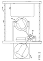
- Fig. 1 is a longitudal cross-section of a substrate treating system, showing a substrate loading station, a substrate cooling fixture, an ion source, and a transport arm.
- Fig. 2 is a top view of the treating system with the process chamber and loading station housing cut away to show the transfer arm in the load station position (solid line) and in the cooling fixture position (dotted line).
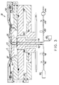
- Fig. 3 is a cross-sectional view of the substrate cooling fixture with a substrate clamped to the fixture and gas flowing between the substrate and the fixture.
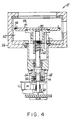
- Fig. 4 is a cross-sectional view of the loading station, excluding the cover and cover actuator.
- Fig. 5a is a plan view of the substrate transfer mechanism.
- Fig. 5b is a cross-sectional view of the substrate transfer mechanism.
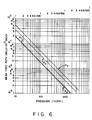
- Fig. 6 is a log-log graph of pressure vs. mean free path of gas molecules for respective Nitrogen, Argon, Hydrogen, and Helium gasses.
- a substrate treating system 10 includes a loading station 12, cooling fixture 14, transport arm 16, ion source 18 and process chamber 20.
- a substrate S is loaded into the loading station 12 and moved by transfer arm 16 onto cooling fixture 14 within the process chamber 20.
- the process chamber is at substantially vacuum pressure (i.e. less than 0.12 Pa (.0009 Torr)).
- the ion source 18 directs an ion beam onto the substrate for processing the substrate (i.e. ion beam etching, reactive ion beam etching, chemically assisted ion beam etching, or other substrate treating process).
- the cooling fixture 14 cools the wafer during treatment by solid-to-solid conduction, free convection and forced convection.
- the loading station cover 24 is raised.
- a manual system an operator inserts the substrate onto substrate holder 28.
- a cassette to cassette automatic feeder or other automatic transport device is used to insert the substrate.
- the cover 24 is then lowered by an actuator 26.
- the substrate within the load station 12 can be seen through a view port 30 in the cover 24.
- an O-ring 32 provides a seal between the load-lock volume 22 and the external environment.
- the substrate holder 28 is connected to the load-lock platform 36 which may be moved up or down.
- a popet-type O-ring seal seals the load-lack volume 22 from the loading station chamber 52.
- the seal enables the load-lock volume 22 to be at atmospheric pressure, while the loading station chamber 52 is at substantially vacuum pressure.
- the load-lock volume 22 pressure is reduced to substantially less than atmospheric pressure.
- platform 36 lowers the substrate into the loading station chamber 52, thereby releasing the seal between the load-lock volume 22 and the chamber 52.
- a brake 38 is deactivated, allowing for rotation of a drive shaft 40.
- a load-lock ball screw 42 moves the platform 36 up or down.
- the drive shaft 40 at approximately atmospheric pressure moves the ball screw 42 at substantially vacuum pressure by transferring a rotational moment through a dynamic seal 44.
- the dynamic seal 44 includes two seal rings 46 housing an external O-ring 48 and an inner O-ring 50.
- the O-ring 48 acts as a seal and also acts as a cushion for absorbing eccentric motion of the shaft 40.
- the volume between the seal rings is differentially pumped.
- the inner O-ring 50 isolates the a vacuum pressure area from an atmospheric pressure area. Such a construction provides a low frictional torque between the shaft 40 and dynamic seal ring 50.
- the loading station chamber 52 is open to the process chamber 20. With the platform 36 in the lower position, the transfer arm 16 having a home position within the process chamber 20 can access the substrate. Referring to Fig. 2, the transport arm 16 moves the substrate from the loading station 12 to the cooling fixture 14. Referring to Figs. 5a and 5B the transport arm 16 includes a spatula-type member 60 connected to a four-bar slider linkage assembly.
- the linkage assembly includes a crank 62, slider block 64, based 66, and rod 68.
- the spatula 60 travels in a horizontal plane, parallel to the plane of the substrate and below such plane of the substrate into the loading chamber 52.
- the spatula 60 is raised vertically, thereby lifting the substrate off the substrate holder 28.
- the spatula then moves in a horizontal plane toward the cooling fixture 14 and loads the substrate into the fixture 14 between the substrate carrier 70 and the clamp 72.
- the substrate carrier 70 and clamp 72 are shown in the down position.
- the clamp 72 may move vertically under the control of clamp actuator 84.
- When loading a substrate the two are in the up position, which has a vertical level above the plane of the substrate seat 86.
- the substrate moves freely between the carrier 70 and the clamp 72.
- the transfer arm 16 is then lowered allowing the substrate to come to rest on the substrate carrier 70.
- the transfer arm moves the substrate to the fixture 14 without the need for clamping or securing the substrate to the spatula.
- the horizontal motion of the transfer arm 16 is accomplished with the four bar slider linkage assembly.
- the assembly uses pin or slider joints.
- a first rotary input shaft 74 results in a horizontal output motion.
- the first rotary input shaft 74 is geared through a miter bevel or other angle drive 76 to drive a linear couple 78.
- the linear couple 78 drives the crank 62 about the crank's pivot point.
- the crank rotation causes, via the rod 68 and slider block 64, a translation and rotation of the spatula 60 in the horizontal plane.
- the slider block 64 has a prismatic motion relative to the rod 68 and a pivot motion relative to the base 66. By providing both prismatic and pivot motion of the slider block 64, the spatula 60 may travel essentially a linear path between the loading station 12 and the cooling fixture 14 with a single rotary input.
- a second rotary input shaft 80 drives a power screw or other rotary axial linear motion device 82 to provide a vertical motion of the linkage assembly and spatula.
- the linear couple 78 allows for verticle displacement of the linkage assembly without disturbing the crank 62 axis of rotation.
- a conventional closed loop servo motor drive subsystem may be used to provide the first and second rotary shaft inputs under the control of a central computer. By using computer control, information on the position of the spatula 60 and substrate may be readily obtained.
- Other input control devices alternatively may be used to provide inputs to the first and second rotary input shafts.
- the transport arm 16 After the substrate has been loaded into the cooling fixture 14, the transport arm 16 returns to a home position. At any time after the transport arm moves the wafer out of the vertical path of the load-lock platform 36 and prior to the start of substrate treatment, the platform 36 is raised to the upper position pressure-isolating the load lock volume 22 from the loading station chamber 52 and preventing exposure of the load-lock volume to the process gases.
- clamp actuator 84 is activated lowering the substrate clamp 72 and substrate carrier 70.
- the substrate rests on the substrate seat 86, then is pressed to the seat 86.
- O-ring 88 i.e. elastomer 40-70 durometer
- other vacuum gas seal near the periphery of the seat 86 provides a substantially vacuum tight seal between the substrate S and the seat 86.
- the substrate clamp 72 holds the substrate firmly to the seat 86 with an adjustable hold-down force which may vary depending on the material and thickness of the substrate. Examples of substrate materials are Silicon, GaAs, Ferrite, AlSiMag, and glass other materials may also be used.
- the size of the substrates may vary, for example, from 5 cm to 15 cm (2 inches to 6 inches) in diameter or from 2.5 cm by 2.5 cm (1 inch by 1 inch) to 15 cm by 15 cm (6 inch by 6 inch) square.
- the substrates need not be a contiguous wafer-like body, but may be fragments mounted on a carrier.
- Substrate thickness may range, for example, from 0.25 mm (.01 inches) to 4.0 millimeters.
- the size, material, and thickness are not limited to the example ranges provided as the invention may be applied for a variety of size, material, and thickness ranges.
- gas from a source 90 is flowed through a gas input channel 92 in the cooling fixture 14 and into and through the region 93 between the substrate S and the seat 86.
- the gas enters the region at the periphery of the seat within the confines of the O-ring 88, travels radially from the periphery to the center of the region, then exits through exit channel 94.
- the gas inlet and outlet can be reversed for various materials and thicknesses. In other embodiments the inlet and outlet positions may vary according to design.
- Gas flow is controlled by a control device 96 such as a throttling value, orifice, or mass flow controller.
- the gas pressure in the region between the substrate and the seat 86 will vary from approximately 1.33 kPa to 101.3 kPa (10 Torr to 760 Torr) and preferably from 2.67 kPa to 101.3 kPa (20 Torr to 760 Torr) depending on the thickness and material of the substrate.
- the gas travels from the source 90 through the control device 96, a shut-off value 98, and the gas input channel 92 before entering the region between the substrate S and the seat 86. While passing through the input channel 92 the gas is cooled to approximately 10°C by the fixture walls.
- the cooling fixture 14 has a circulating cooling fluid such as water for cooling the gas, although other cooling fluids may be used.
- the gas flows from the region 93 through the exit channel 94 and passes through another shut off value 100 and control device 102.
- the gas flow is forced by a gas pump 104.
- a pressure meter 106 signifies the gas pressure.
- the gas molecules While the gas flows radially from the outer diameter to the center of the region 93, the gas molecules absorb heat energy from (i) the back surface of the substrate and (ii) collisions with other gas molecules. This heat energy is transferred out of the region by the flowing of the gas molecules into the exit channel 94. Such heat transfer is a forced convection heat transfer.
- Fig. 6 shows a graph of the mean free path vs pressure for Nitrogen, Argon, Hydrogen, and Helium gases, respectively.
- the mean free path of Argon at a pressure of 3.33 kPa (25 Torr) is approximately 1.93 ⁇ m (.000076 inches).
- the cooling fixture 14 and clamp 72 are cooled via circulating cooling fluid. Heat energy from the substrate is transferred to the clamp by solid-to-solid conduction.
- the cooling fixture 14 may be tilted and rotated during substrate treatment by a rotary actuator 106.
- the treating process time varies from one minute to more than two hours.
- the fixture 14 is positioned at a load position and shut-off valve 98 is closed.
- Gas pump 104 thereby pumps out the gas volume in channels 92 and 94 and in the region between the substrate and the seat.
- the shut off valve 100 is closed.
- the degree of vacuum before ceasing the gas evacuation may vary.
- the clamp actuator 84 raises the substrate clamp 72.
- the substrate is thus lifted from the seat 86 by the substrate carrier 70 which is connected to the clamp 72.
- the transfer arm 16 then travels in a horizontal plane parallel to the substrate and below the plane of the substrate to the cooling fixture 14.
- the link assembly and spatula are raised lifting the substrate off the substrate carrier.
- the load lock volume 22 is pumped down to a substantially vacuum pressure after substrate treatment and prior to movement of the substrate from the area of the cooling fixture 14 to the loading station chamber 52.
- the load-lock platform 86 is lowered to the down position. While the platform 86 is in the down position, the transfer arm 16 moves the spatula with substrate into the loading station chamber 52. The linkage assembly and spatula then is lowered allowing the substrate to rest on the substrate holder 28. The transfer arm 16 then moves back to the home position.
- the load lock platform 86 then moves to the up position pressure-isolating the load-lock volume from the loading station chamber 52.
- the load-lock volume is then vented up to approximately atmospheric pressure without producing significant turbulence.
- the cover actuator 26 then lifts the cover 24 and the operator or an automatic feeder device accesses the treated substrate.
Landscapes
- Container, Conveyance, Adherence, Positioning, Of Wafer (AREA)
- Drying Of Semiconductors (AREA)
- ing And Chemical Polishing (AREA)
Claims (11)
- Verfahren zum Kühlen eines waferartigen Gegenstandes in einer Vakuumkammer, mit den Schritten:Drücken des Gegenstandes (S) gegen einen kühlenden Sitz (86) mittels einer Substratklemme (72);Strömenlassen von unter Druck stehendem Gas in und durch einen Bereich (93) zwischen dem Gegenstand (S) und dem Sitz (86), um die Wärmeübertragung von dem Gegenstand durch Zwangskonvektion zu erleichtern,wobei der Gasdruck in dem Bereich (93) hoch genug ist, um die Wärmeübertragung von dem Gegenstand (S) zu dem Sitz (86) durch freie Konvektion zu erleichtern; und.dadurch gekennzeichnet, daß die Substratklammer (72) durch ein in Kanälen in der Klemme zirkulierendes Kühlfluid gekühlt ist.
- Verfahren nach Anspruch 1, bei dem das Gas von dem kühlenden Sitz (86) gekühlt wird, bevor es in den Bereich (93) zwischen dem Gegenstand (S) und dem Sitz (86) strömt.
- Verfahren nach Anspruch 1, bei dem das Gas radial zwischen den Umfang des Sitzes (86) und den Mittelpunkt des Sitzes (86) strömt.
- Verfahren nach Anspruch 1, bei dem der Gasdruck hoch genug ist, um ein Senken oder Heben des Gegenstandes (S) zu bewirken.
- Verfahren nach Anspruch 1, ferner mit dem Schritt des Pumpens des Gases aus dem Bereich (93) zwischen dem Gegenstand und dem Sitz vor Beendigung des AndrUckens des Gegenstandes gegen den Sitz (86).
- Verfahren nach Anspruch 1, bei dem der Gasdruck konstant gehalten wird und innerhalb eines Bereiches zwischen 1,330 kPa und 101,3 kPa (10 Torr und 760 Torr) liegt, wobei der konstante Druck innerhalb des Bereiches durch das Material, die Größe und die Dicke des Gegenstandes bestimmt wird.
- Vorrichtung zum Kühlen eines waferartigen Gegenstandes (S) in einer Vakuumkammer, mit:einem Substratsitz (86) mit einem Gaseinlaßkanal (92) und einem Gasauslaßkanal (94),einer vertikal verschiebbaren Substratklemme (72) zum Drücken des Gegenstandes (S) gegen den Sitz (86) und zum Kühlen des Gegenstands durch Übertragung von Festkörper zu Festkörper,einer Dichtvorrichtung (88) an dem Sitz (86) zum Bilden einer Dichtung zwischen dem Gegenstand (S) und dem Sitz (86) unter dem Druck der Klemme (72),wobei ein unter Druck stehendes Gas durch den Einlaßkanal (92) in und durch einen Raum (93) zwischen dem Gegenstand (S) und dem Sitz (86) und durch den Auslaßkanal (14) strömen kann, um den Gegenstand durch Zwangskonvektion zu kühlen,wobei der Gegenstand auch durch freie Konvektionswärmeübertragung von dem Gegenstand zum Sitz (86) gekühlt werden kann,dadurch gekennzeichnet, daß Kühlmittelkanäle in der Klemme (72) für das Zirkulieren eines Kühlfluids vorgesehen sind.
- Vorrichtung nach Anspruch 7, ferner mit einer Pumpe (104) zum Drücken des Gasstromes in den Einlaßkanal (92), durch den Bereich (93) zwischen dem Gegenstand (S) und dem Sitz (6) und aus dem Auslaßkanal (94) heraus.
- Vorrichtung nach Anspruch 8, ferner mit einem mit dem Einlaßkanal (92) in Verbindung stehenden Absperrventil (98) zum Sperren des Gasstroms in den Einlaßkanal (92) und durch den Bereich (93) zwischen dem Gegenstand (S) und dem Sitz (86).
- Vorrichtung nach Anspruch 7, ferner mit einer Gasströmungssteuervorrichtung (96) zum Steuern der Strömungsrate des Gascs durch den Bereich (93) zwischen dem Gegenstand (S) und dem Sitz (86).
- Vorrichtung nach Anspruch 7, bei der der Sitz (86) zur Verbesserung des thermischen Wärmeübertragungskoeffizienten eine schwarz eloxierte Fläche aufweist.
Applications Claiming Priority (2)
| Application Number | Priority Date | Filing Date | Title |
|---|---|---|---|
| US07/195,707 US4949783A (en) | 1988-05-18 | 1988-05-18 | Substrate transport and cooling apparatus and method for same |
| US195707 | 1988-05-18 |
Publications (3)
| Publication Number | Publication Date |
|---|---|
| EP0342940A2 EP0342940A2 (de) | 1989-11-23 |
| EP0342940A3 EP0342940A3 (de) | 1991-05-08 |
| EP0342940B1 true EP0342940B1 (de) | 1997-12-03 |
Family
ID=22722447
Family Applications (1)
| Application Number | Title | Priority Date | Filing Date |
|---|---|---|---|
| EP89304958A Expired - Lifetime EP0342940B1 (de) | 1988-05-18 | 1989-05-17 | Vorrichtung und Verfahren zur Kühlung von Substraten |
Country Status (4)
| Country | Link |
|---|---|
| US (1) | US4949783A (de) |
| EP (1) | EP0342940B1 (de) |
| JP (1) | JP2717308B2 (de) |
| DE (2) | DE68928468T2 (de) |
Families Citing this family (95)
| Publication number | Priority date | Publication date | Assignee | Title |
|---|---|---|---|---|
| US5484011A (en) * | 1986-12-19 | 1996-01-16 | Applied Materials, Inc. | Method of heating and cooling a wafer during semiconductor processing |
| US5228501A (en) * | 1986-12-19 | 1993-07-20 | Applied Materials, Inc. | Physical vapor deposition clamping mechanism and heater/cooler |
| US5180000A (en) * | 1989-05-08 | 1993-01-19 | Balzers Aktiengesellschaft | Workpiece carrier with suction slot for a disk-shaped workpiece |
| DE3943478C2 (de) * | 1989-05-08 | 1995-11-16 | Philips Electronics Nv | Werkstückträger für ein scheibenförmiges Werkstück, sowie Vakuumbehandlungsanlage |
| US5673750A (en) * | 1990-05-19 | 1997-10-07 | Hitachi, Ltd. | Vacuum processing method and apparatus |
| KR0165898B1 (ko) * | 1990-07-02 | 1999-02-01 | 미다 가쓰시게 | 진공처리방법 및 장치 |
| USH1145H (en) | 1990-09-25 | 1993-03-02 | Sematech, Inc. | Rapid temperature response wafer chuck |
| EP0491503A3 (de) * | 1990-12-19 | 1992-07-22 | AT&T Corp. | Verfahren zur Ablagerung von Metall |
| US5267607A (en) * | 1991-05-28 | 1993-12-07 | Tokyo Electron Limited | Substrate processing apparatus |
| JP2577162B2 (ja) * | 1991-06-17 | 1997-01-29 | アプライド マテリアルズ インコーポレイテッド | ロードロックチャンバにおける加熱されたシリコン基板に生じる温度差を制御する方法および装置 |
| JPH05166757A (ja) * | 1991-12-13 | 1993-07-02 | Tokyo Electron Ltd | 被処理体の温調装置 |
| US5343012A (en) * | 1992-10-06 | 1994-08-30 | Hardy Walter N | Differentially pumped temperature controller for low pressure thin film fabrication process |
| JPH06204157A (ja) * | 1992-12-25 | 1994-07-22 | Tokyo Electron Tohoku Ltd | 縦型熱処理装置 |
| KR960006958B1 (ko) * | 1993-02-06 | 1996-05-25 | 현대전자산업주식회사 | 이시알 장비 |
| TW277139B (de) * | 1993-09-16 | 1996-06-01 | Hitachi Seisakusyo Kk | |
| US5738751A (en) * | 1994-09-01 | 1998-04-14 | Applied Materials, Inc. | Substrate support having improved heat transfer |
| US5595241A (en) * | 1994-10-07 | 1997-01-21 | Sony Corporation | Wafer heating chuck with dual zone backplane heating and segmented clamping member |
| EP0871843B1 (de) * | 1994-10-17 | 2003-05-14 | Varian Semiconductor Equipment Associates Inc. | Montageelement und methode zum klemmen eines flachen, dünnen und leitfähigen werkstückes |
| TW281795B (de) * | 1994-11-30 | 1996-07-21 | Sharp Kk | |
| US5746930A (en) * | 1995-01-03 | 1998-05-05 | Texas Instruments Incorporated | Method and structure for forming an array of thermal sensors |
| US5603848A (en) * | 1995-01-03 | 1997-02-18 | Texas Instruments Incorporated | Method for etching through a substrate to an attached coating |
| US5626773A (en) * | 1995-01-03 | 1997-05-06 | Texas Instruments Incorporated | Structure and method including dry etching techniques for forming an array of thermal sensitive elements |
| US5605600A (en) * | 1995-03-13 | 1997-02-25 | International Business Machines Corporation | Etch profile shaping through wafer temperature control |
| US5679404A (en) * | 1995-06-07 | 1997-10-21 | Saint-Gobain/Norton Industrial Ceramics Corporation | Method for depositing a substance with temperature control |
| US6140612A (en) | 1995-06-07 | 2000-10-31 | Lam Research Corporation | Controlling the temperature of a wafer by varying the pressure of gas between the underside of the wafer and the chuck |
| US6053982A (en) * | 1995-09-01 | 2000-04-25 | Asm America, Inc. | Wafer support system |
| US6113702A (en) * | 1995-09-01 | 2000-09-05 | Asm America, Inc. | Wafer support system |
| US5775416A (en) * | 1995-11-17 | 1998-07-07 | Cvc Products, Inc. | Temperature controlled chuck for vacuum processing |
| US5697427A (en) * | 1995-12-22 | 1997-12-16 | Applied Materials, Inc. | Apparatus and method for cooling a substrate |
| US5948283A (en) * | 1996-06-28 | 1999-09-07 | Lam Research Corporation | Method and apparatus for enhancing outcome uniformity of direct-plasma processes |
| US5936829A (en) * | 1997-01-02 | 1999-08-10 | Cvc Products, Inc. | Thermally conductive chuck for vacuum processor |
| DE19781631T1 (de) * | 1997-01-02 | 1999-04-01 | Cvc Products Inc | Wärmeleitendes Spannfutter für Vakuumbearbeitungsvorrichtung |
| US6183523B1 (en) | 1997-03-03 | 2001-02-06 | Tokyo Electron Limited | Apparatus for thermal control of variously sized articles in vacuum |
| US6073366A (en) * | 1997-07-11 | 2000-06-13 | Asm America, Inc. | Substrate cooling system and method |
| DE19882662T1 (de) * | 1997-08-28 | 2000-08-03 | Cvc Products Inc | Wafertransportvorrichtung für Mehrstationswerkzeug |
| US6138745A (en) | 1997-09-26 | 2000-10-31 | Cvc Products, Inc. | Two-stage sealing system for thermally conductive chuck |
| US6073576A (en) | 1997-11-25 | 2000-06-13 | Cvc Products, Inc. | Substrate edge seal and clamp for low-pressure processing equipment |
| EP1057214A1 (de) | 1998-02-18 | 2000-12-06 | Applied Materials, Inc. | Greifer für einen wafer-manipulator in einem behandlungssystem |
| US6545580B2 (en) | 1998-09-09 | 2003-04-08 | Veeco Instruments, Inc. | Electromagnetic field generator and method of operation |
| US6108937A (en) * | 1998-09-10 | 2000-08-29 | Asm America, Inc. | Method of cooling wafers |
| US6957690B1 (en) | 1998-09-10 | 2005-10-25 | Asm America, Inc. | Apparatus for thermal treatment of substrates |
| KR100634642B1 (ko) * | 1998-11-20 | 2006-10-16 | 스티그 알티피 시스템즈, 인코포레이티드 | 반도체 웨이퍼의 급속 가열 및 냉각 장치 |
| US6110288A (en) * | 1998-12-17 | 2000-08-29 | Eaton Corporation | Temperature probe and measurement method for low pressure process |
| DE19907210A1 (de) * | 1999-02-23 | 2000-08-31 | Krauss Maffei Kunststofftech | Vorrichtung zum Transportieren und gleichzeitigen Kühlen von Substraten für Informationsträgerscheiben wie CD, DVD oder dergleichen |
| US6241005B1 (en) | 1999-03-30 | 2001-06-05 | Veeco Instruments, Inc. | Thermal interface member |
| US6635580B1 (en) * | 1999-04-01 | 2003-10-21 | Taiwan Semiconductor Manufacturing Co. Ltd. | Apparatus and method for controlling wafer temperature in a plasma etcher |
| WO2000074117A1 (en) | 1999-05-27 | 2000-12-07 | Matrix Integrated Systems, Inc. | Rapid heating and cooling of workpiece chucks |
| JP2001068538A (ja) * | 1999-06-21 | 2001-03-16 | Tokyo Electron Ltd | 電極構造、載置台構造、プラズマ処理装置及び処理装置 |
| DE19949005A1 (de) * | 1999-10-11 | 2001-05-10 | Leica Microsystems | Einrichtung und Verfahren zum Einbringen verschiedener transparenter Substrate in ein hochgenaues Messgerät |
| US6705394B1 (en) | 1999-10-29 | 2004-03-16 | Cvc Products, Inc. | Rapid cycle chuck for low-pressure processing |
| US6259062B1 (en) | 1999-12-03 | 2001-07-10 | Asm America, Inc. | Process chamber cooling |
| US6290491B1 (en) | 2000-06-29 | 2001-09-18 | Motorola, Inc. | Method for heating a semiconductor wafer in a process chamber by a shower head, and process chamber |
| US6652655B1 (en) * | 2000-07-07 | 2003-11-25 | Applied Materials, Inc. | Method to isolate multi zone heater from atmosphere |
| US6689221B2 (en) * | 2000-12-04 | 2004-02-10 | Applied Materials, Inc. | Cooling gas delivery system for a rotatable semiconductor substrate support assembly |
| US6609869B2 (en) | 2001-01-04 | 2003-08-26 | Asm America | Transfer chamber with integral loadlock and staging station |
| US6470946B2 (en) | 2001-02-06 | 2002-10-29 | Anadigics, Inc. | Wafer demount gas distribution tool |
| US6491083B2 (en) | 2001-02-06 | 2002-12-10 | Anadigics, Inc. | Wafer demount receptacle for separation of thinned wafer from mounting carrier |
| US6899507B2 (en) * | 2002-02-08 | 2005-05-31 | Asm Japan K.K. | Semiconductor processing apparatus comprising chamber partitioned into reaction and transfer sections |
| US20030168174A1 (en) * | 2002-03-08 | 2003-09-11 | Foree Michael Todd | Gas cushion susceptor system |
| US7208195B2 (en) * | 2002-03-27 | 2007-04-24 | Ener1Group, Inc. | Methods and apparatus for deposition of thin films |
| US6547559B1 (en) | 2002-05-20 | 2003-04-15 | Veeco Instruments, Inc. | Clamping of a semiconductor substrate for gas-assisted heat transfer in a vacuum chamber |
| AU2003270613A1 (en) * | 2002-09-10 | 2004-04-30 | Axcelis Technologies, Inc. | Method of heating a substrate in a variable temperature process using a fixed temperature chuck |
| US7169231B2 (en) * | 2002-12-13 | 2007-01-30 | Lam Research Corporation | Gas distribution system with tuning gas |
| US7481312B2 (en) * | 2004-12-02 | 2009-01-27 | Hitachi Global Storage Technologies Netherlands B.V. | Direct cooling pallet assembly for temperature stability for deep ion mill etch process |
| US7296420B2 (en) * | 2004-12-02 | 2007-11-20 | Hitachi Global Storage Technologies Amsterdam, B.V. | Direct cooling pallet tray for temperature stability for deep ion mill etch process |
| US20080314320A1 (en) * | 2005-02-04 | 2008-12-25 | Component Re-Engineering Company, Inc. | Chamber Mount for High Temperature Application of AIN Heaters |
| US20100270004A1 (en) * | 2005-05-12 | 2010-10-28 | Landess James D | Tailored profile pedestal for thermo-elastically stable cooling or heating of substrates |
| JP4666473B2 (ja) * | 2005-05-12 | 2011-04-06 | 大日本スクリーン製造株式会社 | 基板熱処理装置 |
| EP2495212A3 (de) * | 2005-07-22 | 2012-10-31 | QUALCOMM MEMS Technologies, Inc. | MEMS-Vorrichtungen mit Stützstrukturen und Herstellungsverfahren dafür |
| US9127362B2 (en) * | 2005-10-31 | 2015-09-08 | Applied Materials, Inc. | Process kit and target for substrate processing chamber |
| US7918938B2 (en) * | 2006-01-19 | 2011-04-05 | Asm America, Inc. | High temperature ALD inlet manifold |
| US20070209593A1 (en) * | 2006-03-07 | 2007-09-13 | Ravinder Aggarwal | Semiconductor wafer cooling device |
| US20070283709A1 (en) * | 2006-06-09 | 2007-12-13 | Veeco Instruments Inc. | Apparatus and methods for managing the temperature of a substrate in a high vacuum processing system |
| US7763869B2 (en) * | 2007-03-23 | 2010-07-27 | Asm Japan K.K. | UV light irradiating apparatus with liquid filter |
| US8092606B2 (en) * | 2007-12-18 | 2012-01-10 | Asm Genitech Korea Ltd. | Deposition apparatus |
| TWI472882B (zh) * | 2008-05-06 | 2015-02-11 | 諾菲勒斯系統公司 | 光阻剝離方法及設備 |
| WO2010026772A1 (ja) * | 2008-09-04 | 2010-03-11 | キヤノンアネルバ株式会社 | 基板冷却方法及び半導体の製造方法 |
| KR20110097908A (ko) * | 2008-11-28 | 2011-08-31 | 볼커 프로브스트 | 반도체 층 또는 원소 셀레늄 및/또는 황으로 처리된 코팅 기판, 특히 평면 기판의 제조 방법 |
| US8033771B1 (en) | 2008-12-11 | 2011-10-11 | Novellus Systems, Inc. | Minimum contact area wafer clamping with gas flow for rapid wafer cooling |
| US8297342B2 (en) * | 2009-06-29 | 2012-10-30 | International Business Machines Corporation | Heat sink assembly |
| CN101988191B (zh) * | 2010-12-01 | 2012-05-16 | 东莞宏威数码机械有限公司 | 基板卸载装置及卸载方法 |
| US8371567B2 (en) | 2011-04-13 | 2013-02-12 | Novellus Systems, Inc. | Pedestal covers |
| US9574268B1 (en) | 2011-10-28 | 2017-02-21 | Asm America, Inc. | Pulsed valve manifold for atomic layer deposition |
| US9388492B2 (en) | 2011-12-27 | 2016-07-12 | Asm America, Inc. | Vapor flow control apparatus for atomic layer deposition |
| WO2013103594A1 (en) | 2012-01-06 | 2013-07-11 | Novellus Systems, Inc. | Adaptive heat transfer methods and systems for uniform heat transfer |
| CN104037113B (zh) * | 2013-03-04 | 2018-05-08 | 中微半导体设备(上海)有限公司 | 等离子体处理腔室的供气装置以及去夹持方法 |
| US9378992B2 (en) * | 2014-06-27 | 2016-06-28 | Axcelis Technologies, Inc. | High throughput heated ion implantation system and method |
| US9607803B2 (en) | 2015-08-04 | 2017-03-28 | Axcelis Technologies, Inc. | High throughput cooled ion implantation system and method |
| DE112016006567B4 (de) * | 2016-03-10 | 2022-12-29 | Mitsubishi Electric Corporation | Substratansaugstufe, substratbehandlungsvorrichtung und substratbehandlungsverfahren |
| US10662527B2 (en) | 2016-06-01 | 2020-05-26 | Asm Ip Holding B.V. | Manifolds for uniform vapor deposition |
| US10347547B2 (en) | 2016-08-09 | 2019-07-09 | Lam Research Corporation | Suppressing interfacial reactions by varying the wafer temperature throughout deposition |
| US11492701B2 (en) | 2019-03-19 | 2022-11-08 | Asm Ip Holding B.V. | Reactor manifolds |
| US12516414B2 (en) | 2019-03-19 | 2026-01-06 | Asm Ip Holding B.V. | Reactor manifolds |
| KR20210048408A (ko) | 2019-10-22 | 2021-05-03 | 에이에스엠 아이피 홀딩 비.브이. | 반도체 증착 반응기 매니폴드 |
| CN120048763B (zh) * | 2025-02-20 | 2025-11-14 | 盛红晔半导体科技(上海)有限公司 | 一种基于稀薄换热机制的晶圆冷却系统及方法 |
Citations (1)
| Publication number | Priority date | Publication date | Assignee | Title |
|---|---|---|---|---|
| EP0219826A2 (de) * | 1985-10-24 | 1987-04-29 | Texas Instruments Incorporated | System für Vakuumbehandlung |
Family Cites Families (23)
| Publication number | Priority date | Publication date | Assignee | Title |
|---|---|---|---|---|
| US3566960A (en) * | 1969-08-18 | 1971-03-02 | Robley V Stuart | Cooling apparatus for vacuum chamber |
| CH544274A (de) * | 1971-10-27 | 1973-11-15 | Balzers Patent Beteilig Ag | Einrichtung zum Kühlen von Werkstücken, die einer Behandlung im Vakuum unterworfen werden |
| JPS5016076A (de) * | 1973-06-18 | 1975-02-20 | ||
| US4072188A (en) * | 1975-07-02 | 1978-02-07 | Honeywell Information Systems Inc. | Fluid cooling systems for electronic systems |
| US3993123A (en) * | 1975-10-28 | 1976-11-23 | International Business Machines Corporation | Gas encapsulated cooling module |
| US4139051A (en) * | 1976-09-07 | 1979-02-13 | Rockwell International Corporation | Method and apparatus for thermally stabilizing workpieces |
| US4194233A (en) * | 1978-01-30 | 1980-03-18 | Rockwell International Corporation | Mask apparatus for fine-line lithography |
| US4282924A (en) * | 1979-03-16 | 1981-08-11 | Varian Associates, Inc. | Apparatus for mechanically clamping semiconductor wafer against pliable thermally conductive surface |
| EP0017472A1 (de) * | 1979-04-06 | 1980-10-15 | Lintott Engineering Limited | Vakuumapparatur mit einer Vorrichtung zur Wärmeübertragung und Verfahren zur Herstellung von Halbleiterkomponenten unter Anwendung dieser Apparatus |
| US4261762A (en) * | 1979-09-14 | 1981-04-14 | Eaton Corporation | Method for conducting heat to or from an article being treated under vacuum |
| US4680061A (en) * | 1979-12-21 | 1987-07-14 | Varian Associates, Inc. | Method of thermal treatment of a wafer in an evacuated environment |
| JPS57206046A (en) * | 1981-06-15 | 1982-12-17 | Hitachi Ltd | Wafer conveying device |
| US4457359A (en) * | 1982-05-25 | 1984-07-03 | Varian Associates, Inc. | Apparatus for gas-assisted, solid-to-solid thermal transfer with a semiconductor wafer |
| US4508161A (en) * | 1982-05-25 | 1985-04-02 | Varian Associates, Inc. | Method for gas-assisted, solid-to-solid thermal transfer with a semiconductor wafer |
| JPS5913327A (ja) * | 1982-07-15 | 1984-01-24 | Toshiba Corp | ドライエツチング装置 |
| JPS5994435A (ja) * | 1982-11-20 | 1984-05-31 | Tokuda Seisakusho Ltd | 真空処理装置 |
| JPS59154386A (ja) * | 1983-02-23 | 1984-09-03 | 株式会社東芝 | 核融合装置のバンパリミタ |
| US4542298A (en) * | 1983-06-09 | 1985-09-17 | Varian Associates, Inc. | Methods and apparatus for gas-assisted thermal transfer with a semiconductor wafer |
| JPH0622213B2 (ja) * | 1983-11-28 | 1994-03-23 | 株式会社日立製作所 | 試料の温度制御方法及び装置 |
| US4603466A (en) * | 1984-02-17 | 1986-08-05 | Gca Corporation | Wafer chuck |
| US4567938A (en) * | 1984-05-02 | 1986-02-04 | Varian Associates, Inc. | Method and apparatus for controlling thermal transfer in a cyclic vacuum processing system |
| JPS6130237U (ja) * | 1984-07-26 | 1986-02-24 | 日立電子エンジニアリング株式会社 | ウエハ処理装置のウエハロ−ド機構 |
| JPS6261334A (ja) * | 1985-09-11 | 1987-03-18 | Hitachi Ltd | パタ−ンの形成方法 |
-
1988
- 1988-05-18 US US07/195,707 patent/US4949783A/en not_active Expired - Lifetime
-
1989
- 1989-05-17 EP EP89304958A patent/EP0342940B1/de not_active Expired - Lifetime
- 1989-05-17 DE DE68928468T patent/DE68928468T2/de not_active Expired - Lifetime
- 1989-05-17 DE DE0342940T patent/DE342940T1/de active Pending
- 1989-05-18 JP JP12546789A patent/JP2717308B2/ja not_active Expired - Lifetime
Patent Citations (1)
| Publication number | Priority date | Publication date | Assignee | Title |
|---|---|---|---|---|
| EP0219826A2 (de) * | 1985-10-24 | 1987-04-29 | Texas Instruments Incorporated | System für Vakuumbehandlung |
Also Published As
| Publication number | Publication date |
|---|---|
| EP0342940A3 (de) | 1991-05-08 |
| EP0342940A2 (de) | 1989-11-23 |
| DE342940T1 (de) | 1995-06-08 |
| DE68928468D1 (de) | 1998-01-15 |
| US4949783A (en) | 1990-08-21 |
| DE68928468T2 (de) | 1998-07-02 |
| JPH0230128A (ja) | 1990-01-31 |
| JP2717308B2 (ja) | 1998-02-18 |
Similar Documents
| Publication | Publication Date | Title |
|---|---|---|
| EP0342940B1 (de) | Vorrichtung und Verfahren zur Kühlung von Substraten | |
| KR100613171B1 (ko) | 반도체 기판 냉각 방법 및 장치 | |
| US6602348B1 (en) | Substrate cooldown chamber | |
| US6468353B1 (en) | Method and apparatus for improved substrate handling | |
| US6276072B1 (en) | Method and apparatus for heating and cooling substrates | |
| US5199483A (en) | Method and apparatus for cooling wafers | |
| US6486444B1 (en) | Load-lock with external staging area | |
| KR930008522B1 (ko) | 열전달 제어장치 및 방법 | |
| US5766824A (en) | Method and apparatus for curing photoresist | |
| US6575737B1 (en) | Method and apparatus for improved substrate handling | |
| CN100435269C (zh) | 处理系统 | |
| US5511608A (en) | Clampless vacuum heat transfer station | |
| US4508161A (en) | Method for gas-assisted, solid-to-solid thermal transfer with a semiconductor wafer | |
| US4567938A (en) | Method and apparatus for controlling thermal transfer in a cyclic vacuum processing system | |
| US4457359A (en) | Apparatus for gas-assisted, solid-to-solid thermal transfer with a semiconductor wafer | |
| JP2003526895A (ja) | 真空処理装置においてウェーハを前処理及び後処理するための枚葉式ウェーハロードロックチャンバ | |
| KR20020015966A (ko) | 수직열처리장치와 수직열처리장치의 제어방법 및피처리체를 운송하는 방법 | |
| KR100639071B1 (ko) | 박막 작성 시스템 | |
| KR19980032491A (ko) | 고진공 상태의 2단계 하중 억제 장치와 이를 이용한 웨이퍼 장전 및 인출 방법 | |
| JP2004523880A (ja) | 処理装置用ダブル二重スロット式ロードロック | |
| US6698718B2 (en) | Rotary valve | |
| JPH11233598A (ja) | ウェハ冷却装置 | |
| KR20160086271A (ko) | 접합 장치, 접합 시스템, 접합 방법, 및 컴퓨터 기억 매체 | |
| JP3432721B2 (ja) | 基板冷却装置及び基板冷却方法 | |
| JPH0661329A (ja) | ウエハ処理装置のロードロック機構 |
Legal Events
| Date | Code | Title | Description |
|---|---|---|---|
| PUAI | Public reference made under article 153(3) epc to a published international application that has entered the european phase |
Free format text: ORIGINAL CODE: 0009012 |
|
| AK | Designated contracting states |
Kind code of ref document: A2 Designated state(s): DE FR GB |
|
| PUAL | Search report despatched |
Free format text: ORIGINAL CODE: 0009013 |
|
| AK | Designated contracting states |
Kind code of ref document: A3 Designated state(s): DE FR GB |
|
| 17P | Request for examination filed |
Effective date: 19910926 |
|
| 17Q | First examination report despatched |
Effective date: 19930805 |
|
| EL | Fr: translation of claims filed | ||
| DET | De: translation of patent claims | ||
| GRAG | Despatch of communication of intention to grant |
Free format text: ORIGINAL CODE: EPIDOS AGRA |
|
| GRAG | Despatch of communication of intention to grant |
Free format text: ORIGINAL CODE: EPIDOS AGRA |
|
| GRAH | Despatch of communication of intention to grant a patent |
Free format text: ORIGINAL CODE: EPIDOS IGRA |
|
| GRAH | Despatch of communication of intention to grant a patent |
Free format text: ORIGINAL CODE: EPIDOS IGRA |
|
| GRAA | (expected) grant |
Free format text: ORIGINAL CODE: 0009210 |
|
| AK | Designated contracting states |
Kind code of ref document: B1 Designated state(s): DE FR GB |
|
| REF | Corresponds to: |
Ref document number: 68928468 Country of ref document: DE Date of ref document: 19980115 |
|
| ET | Fr: translation filed | ||
| PLBE | No opposition filed within time limit |
Free format text: ORIGINAL CODE: 0009261 |
|
| STAA | Information on the status of an ep patent application or granted ep patent |
Free format text: STATUS: NO OPPOSITION FILED WITHIN TIME LIMIT |
|
| 26N | No opposition filed | ||
| REG | Reference to a national code |
Ref country code: GB Ref legal event code: IF02 |
|
| PGFP | Annual fee paid to national office [announced via postgrant information from national office to epo] |
Ref country code: DE Payment date: 20080530 Year of fee payment: 20 |
|
| PGFP | Annual fee paid to national office [announced via postgrant information from national office to epo] |
Ref country code: GB Payment date: 20080407 Year of fee payment: 20 |
|
| REG | Reference to a national code |
Ref country code: GB Ref legal event code: PE20 Expiry date: 20090516 |
|
| PG25 | Lapsed in a contracting state [announced via postgrant information from national office to epo] |
Ref country code: GB Free format text: LAPSE BECAUSE OF EXPIRATION OF PROTECTION Effective date: 20090516 |
|
| PGFP | Annual fee paid to national office [announced via postgrant information from national office to epo] |
Ref country code: FR Payment date: 20080424 Year of fee payment: 20 |