US4542298A - Methods and apparatus for gas-assisted thermal transfer with a semiconductor wafer - Google Patents
Methods and apparatus for gas-assisted thermal transfer with a semiconductor wafer Download PDFInfo
- Publication number
- US4542298A US4542298A US06/502,812 US50281283A US4542298A US 4542298 A US4542298 A US 4542298A US 50281283 A US50281283 A US 50281283A US 4542298 A US4542298 A US 4542298A
- Authority
- US
- United States
- Prior art keywords
- wafer
- gas
- thermal transfer
- platen
- intermediate region
- Prior art date
- Legal status (The legal status is an assumption and is not a legal conclusion. Google has not performed a legal analysis and makes no representation as to the accuracy of the status listed.)
- Expired - Lifetime
Links
Images

Classifications
-
- H—ELECTRICITY
- H01—ELECTRIC ELEMENTS
- H01J—ELECTRIC DISCHARGE TUBES OR DISCHARGE LAMPS
- H01J37/00—Discharge tubes with provision for introducing objects or material to be exposed to the discharge, e.g. for the purpose of examination or processing thereof
- H01J37/02—Details
- H01J37/18—Vacuum locks ; Means for obtaining or maintaining the desired pressure within the vessel
-
- H—ELECTRICITY
- H01—ELECTRIC ELEMENTS
- H01L—SEMICONDUCTOR DEVICES NOT COVERED BY CLASS H10
- H01L21/00—Processes or apparatus adapted for the manufacture or treatment of semiconductor or solid state devices or of parts thereof
- H01L21/67—Apparatus specially adapted for handling semiconductor or electric solid state devices during manufacture or treatment thereof; Apparatus specially adapted for handling wafers during manufacture or treatment of semiconductor or electric solid state devices or components ; Apparatus not specifically provided for elsewhere
- H01L21/683—Apparatus specially adapted for handling semiconductor or electric solid state devices during manufacture or treatment thereof; Apparatus specially adapted for handling wafers during manufacture or treatment of semiconductor or electric solid state devices or components ; Apparatus not specifically provided for elsewhere for supporting or gripping
- H01L21/6838—Apparatus specially adapted for handling semiconductor or electric solid state devices during manufacture or treatment thereof; Apparatus specially adapted for handling wafers during manufacture or treatment of semiconductor or electric solid state devices or components ; Apparatus not specifically provided for elsewhere for supporting or gripping with gripping and holding devices using a vacuum; Bernoulli devices
Definitions
- This invention relates to processing of semiconductor wafers in a vacuum chamber and, more particularly, to methods and apparatus for gas-assisted thermal transfer utilizing differential vacuum pumping to reduce gas leakage into the vacuum chamber.
- a major objective is to achieve a high throughput in terms of wafers processed per unit time.
- One way to achieve high throughput in an ion beam system is to use a relatively high power beam. Large amounts of heat may be generated. Thus, it is necessary to provide cooling of the wafer in order to prevent elevated temperatures from being attained.
- Gas-assisted, solid-to-solid thermal transfer with semiconductor wafer is disclosed in pending application Ser. No. 381,669, filed May 25, 1982, and assigned to the assignee of the present application.
- a semiconductor wafer is clamped at its periphery onto a shaped platen.
- Gas under pressure is introduced into the microscopic void region between the platen and the wafer.
- the gas presssure approaches that of the preloading clamping pressure without any appreciable increase in the wafer-to-platen spacing. Since the gas pressure is significantly increased without any increase in the wafer-to-platen gap, the thermal resistance is reduced, and solid-to-solid thermal transfer with gas assistance produces optimum results.
- elastomer O-rings have been utilized to isolate the region containing the thermal transfer gas from the vacuum chamber.
- an O-ring is positioned between the backside of the wafer and the platen near the wafer periphery. While this arrangement provides generally satisfactory sealing, it has certain drawbacks. Due to the elevated temperatures, the wafer can stick to the O-ring, thereby causing an interruption in processing. Furthermore, the O-ring must be located substantially inward of the wafer edge to avoid the wafer flat used for crystal orientation. Therefore, the outer edge portion of the wafer is not cooled.
- the apparatus comprises structure defining an intermediate region adjacent the wafer and isolated from the external environment and platen means including means for supporting the wafer in a processing position with its front surface exposed to the vacuum chamber.
- the platen means further includes means for introduction of a gas at a prescribed pressure into a thermal transfer region between the rear surface of the wafer and the platen means and first restriction means operative to restrict the flow of gas between the thermal transfer region and the intermediate region.
- the apparatus further comprises second restriction means for restricting the flow of gas between the intermediate region and the vacuum chamber and vacuum pumping means coupled to the intermediate region and operative to maintain the intermediate region at a pressure below the prescribed pressure of the gas in the thermal transfer region during processing. Leakage of the gas into the vacuum chamber is thereby reduced.
- a method for gas-assisted thermal transfer with a semiconductor wafer during processing in a vacuum chamber comprises positioning the wafer on a platen in a processing position with the front surface of the wafer exposed to the vacuum chamber and introducing a gas at a prescribed pressure into a thermal transfer region between the rear surface of the wafer and the platen.
- Structure defining an intermediate region is provided adjacent the wafer and isolated from the external environment. The flow of gas between the thermal transfer region and the intermediate region is restricted, and the flow of gas between the intermediate region and the vacuum chamber is restricted.
- the intermediate region is vacuum pumped so as to maintain the pressure therein below the prescribed pressure of the gas in the thermal transfer region and thereby reduce leakage of the gas into the vacuum chamber.
- FIG. 1 is a schematic diagram viewed from above of an ion implantation system incorporating the present invention.
- FIG. 2 is a cross-sectional view of apparatus for gas-assisted thermal transfer with a semiconductor wafer in accordance with the present invention.
- FIG. 1 An ion implantation system suitable for incorporation of the apparatus of the present invention is illustrated in FIG. 1.
- a high voltage terminal 2 is held at high potential relative to ground by a high voltage power supply (not shown).
- the terminal 2 houses the apparatus required to form a beam of ions of desired species.
- a gaseous feedstock of the desired species is employed.
- a source gas produced from a gas handling system 6 is directed to an ion source 8 which is powered by a power supply 10 and provides a high current ion beam 18.
- Ion source techniques are generally known in the art.
- the ion beam 18 diverging from the ion source 8 is mass analyzed and focused by an analyzer magnet 20.
- the analyzed beam passes through a resolving aperture 22 and a variable slit 24 and then through an acceleration tube 26 where it encounters a carefully designed field gradient from the high voltage terminal 2 to ground potential.
- Optical elements such as quadrupole lens 28 operate to produce a spatial energy focus at a target plane.
- Y deflection plates 40 and X deflection plates 42 provide electrostatic deflection which directs the beam 18 over the area of the target plane.
- the waveforms applied to the respective deflection plates, to form the desired scanning pattern, are provided by a scanning system 44.
- a dual target chamber 46 includes a housing, beam defining masks 48, 49 and Faraday cages 50, 51 for beam monitoring.
- Automatic wafer transfer systems 52, 54 introduce semiconductor wafers one at a time into the vacuum system in target positions 56, 58, respectively, align the same with respect to the target plane, provide cooling of the wafers during implantation and remove the wafers from the vacuum system after implantation is complete.
- the target positions 56, 58 are typically located within air locks and are displaced horizontally on opposite sides of the longitudinal axis 60 of the undeflected beam 18, such as to require a beam deflection of about ⁇ 7° from the longitudinal axis for scanning thereof.
- a beam dump 62 is located on the longitudinal axis 60 in the target chamber 46 and intercepts the neutral portion of the ion beam 18.
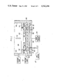
- FIG. 2 there is shown apparatus for gas-assisted thermal transfer with a semiconductor wafer in accordance with the present invention.
- the apparatus can be utilized in the ion implantation system of FIG. 1.
- the target region of the ion implantation system is illustrated in simplified cross-sectional view.
- a platen 100 provides support for a semiconductor wafer 102 in a processing position with its front surface exposed to a vacuum chamber 104.
- the position of the wafer 102 corresponds to the target positions 56, 58 shown in FIG. 1; and the vacuum chamber 104 corresponds to the vacuum chamber 46 shown in FIG. 1.
- the platen 100 is typically a metal, such as aluminum, and can include a curved surface 106, as described in U.S. Pat. No. 4,282,924 and pending application Ser.
- the platen 100 can be attached to, or can be part of, a chamber door 108.
- An O-ring 110 on the chamber door 108 seals the platen 100 into the vacuum chamber 104.
- an ion beam 112 impinges on the wafer 102 and generates heat therein.
- the wafer 102 is in contact with the curved surface 106 in order to remove the heat by conduction.
- the back surface of the wafer 102 and the surface 106 actually make contact over less than 5% of the total area due to microscopic surface irregularities. Numerous microscopic voids exist between the actual points of contact. When these voids are evacuated, heat conduction is greatly reduced.
- a gas such as air, at a prescribed pressure is introduced into the microscopic voids by means of an annular groove 114 in the surface 106 coupled to a passage 116.
- the passage 116 is coupled through a shutoff valve 118 to a gas source 120 at the prescribed pressure, which is typically in the range between one Torr and fifty Torr.
- the gas-filled microscopic voids comprise a thermal transfer region which conducts heat between the wafer 102 and the platen 100. Further details on the technique of gas-assisted thermal transfer are disclosed in pending application Ser. No. 381,669.
- the platen 100 can be provided with passages 122 for circulation of a coolant such as water.
- a spring-loaded clamping ring 130 is attached to a flange 132 which is part of the housing 105. When the platen 100 is in the processing position, the clamping ring 130 securely clamps the wafer 102 against the surface 106.
- a cylindrical bellows 134 is coupled between the flange 132 and the clamping ring 130 and functions as described hereinafter.
- Housing structure adjacent to the platen 100 and the wafer 102 defines an intermediate region 140 surrounding the platen 100 and the wafer 102.
- the structure defining the region 140 can be an integral part of the housing 105 or it can be a separate structural member attached to the housing 105.
- the intermediate region 140 is isolated from the external environment by the O-ring 110 and is isolated from the vacuum chamber 104 by the clamping ring 130 and the bellows 134. While the contact between the clamping ring 130 and the wafer 102 does not provide a high quality vacuum seal, the arrangement restricts the flow of gas between the intermediate region 140 and the vacuum chamber 104. Furthermore, the clamping ring 130 presses the wafer 102 against the surface 106, thereby creating a restriction to the flow of gas between the thermal transfer region behind the wafer 102 and the intermediate region 140.
- the intermediate region 140 is coupled to a vacuum pump 142.
- the vacuum chamber 104 and the platen 100 are separated by a vacuum gate valve 143, thereby creating an air lock which permits wafers to be exchanged without venting the vacuum chamber 104.
- the chamber door 108 and the platen 100 are coupled to a position control means 144 which is operative to open the door 108 from the wafer processing position, as shown in FIG. 2, to a wafer transfer position in which wafers are exchanged.
- the control means 144 can, for example, be an air cylinder.
- the door 108 is opened and a wafer is placed on the surface 106 of the platen 100 and can be retained thereon by a vacuum chuck (not shown) until the door 108 is closed.
- the clamping ring 130 bears against the wafer 102 around its outer periphery and securely clamps the wafer against the platen 100.
- the air lock defined by the vacuum gate valve 143 is vacuum pumped to the approximate pressure of the vacuum chamber 104; and the gate valve 143 is opened.
- the valve 118 is opened, thereby permitting introduction of gas at the prescribed pressure in the thermal transfer region between the wafer 102 and the platen 100.
- Ion implantation of the wafer 102 now proceeds by scanning of the ion beam 112 over the surface of the wafer. Heat imparted to the wafer 102 by the ion beam 112 is transferred to the platen 100 by the gas in the thermal transfer region and by direct conduction at the points of physical contact is then removed from the platen 100 by the coolant circulating through the passages 122.
- the clamping ring 130 clamps the wafer 102 against the surface 106, thereby restricting the flow of the thermal transfer gas from the thermal transfer region into the intermediate region 140.
- contact between the wafer 102 and the surface 106 is not complete; and microscopic voids exist. Therefore, gas is able to escape from the thermal transfer region into the intermediate region 140 but at a relatively low conductance level.
- the vacuum pump 142 can maintain the pressure in the intermediate region 140 substantially below the pressure in the thermal transfer region.
- the clamping ring 130 and the bellows 134 constitute a restriction to flow of gas between the intermediate region 140 and the vacuum chamber 104.
- the seal around the outer periphery of the wafer 102 creates a region low conductance between the intermediate region 140 and the vacuum chamber 104. Since the intermediate region 140 is maintained at a pressure substantially lower than the pressure of the gas in the thermal transfer region, the flow rate of gas into the vacuum chamber 104 is substantially reduced in comparison with prior art systems. Preferably, the pressure in the intermediate region 140 is less than one-tenth the pressure of the gas in the thermal transfer region behind the wafer 102. In practice, the pressure in the intermediate region 140 can be in the range between 1 ⁇ 10 -3 Torr and 0.2 Torr. Thus, there is provided an efficient differential pumping arrangement to insure that the gas used for thermal transfer between the wafer 102 and the platen 100 does not escape in substantial quantity into the vacuum chamber 104.
- the intermediate region 140 provides differential pumping of the thermal transfer gas.
- the intermediate region 140 is isolated from the thermal transfer region by a first restriction means and is isolated from the vacuum chamber 104 by a second restriction means.
- the first and second restriction means can have various forms within the scope of the present invention.
- the bellows 134 can be replaced by a flexible membrane 150, as indicated by dashed lines in FIG. 2 extending radially outward from the clamping ring 130 to the housing 105.
- the wafer 102 can be clamped directly against the flange 132 to restrict the flow of gas from the intermediate region 140 to the vacuum chamber 104.
- the chamber door 108 should have spring loading or other flexible means for clamping the wafer to compensate for mechanical tolerances.
- the platen 100 can be hydraulically actuated, as described co-pending application Ser. No. 324,512, filed Nov. 24, 1981, and assigned to the assignee of the present invention.
- the platen can also have other configurations.
- a cavity can be provided behind the wafer 102 for introduction of gas, as disclosed in U.S. Pat. No. 4,264,762. The gas is restricted from flowing into the intermediate region 140 by a raised annular portion of the platen around the outer periphery of the wafer or by an O-ring.
- the gas can be introduced in the center of the wafer or at any other convenient location.
- the annular groove shown in FIG. 2 improves the uniformity of gas pressure behind the wafer.
- the clamping ring 130 can be dimensioned to clamp the wafer 102 very close to its outer edge, since no O-ring is used for sealing the wafer.
- the clamping ring 130 can have a flat portion to correspond to the wafer flat, thereby insuring clamping at the outermost periphery of the wafer 102.
- an optical elastomer O-ring 160 can be provided in the platen 100 radially outward of the annular groove 114 for more complete sealing between the thermal transfer region and the intermediate region 140. While the O-ring has certain drawbacks, as described hereinabove, its use may be desirable in certain situations, for example, when the vacuum chamber 104 utilizes ultrahigh vacuum and leakage must be minimized.
- the present invention has been described with reference to cooling of the semiconductor wafer or other workpieces. In some applications, heating of the workpiece utilizing a thermal transfer gas may be required. The present invention is equally applicable to such situations.
Abstract
Description
Claims (14)
Priority Applications (1)
| Application Number | Priority Date | Filing Date | Title |
|---|---|---|---|
| US06/502,812 US4542298A (en) | 1983-06-09 | 1983-06-09 | Methods and apparatus for gas-assisted thermal transfer with a semiconductor wafer |
Applications Claiming Priority (1)
| Application Number | Priority Date | Filing Date | Title |
|---|---|---|---|
| US06/502,812 US4542298A (en) | 1983-06-09 | 1983-06-09 | Methods and apparatus for gas-assisted thermal transfer with a semiconductor wafer |
Publications (1)
| Publication Number | Publication Date |
|---|---|
| US4542298A true US4542298A (en) | 1985-09-17 |
Family
ID=23999520
Family Applications (1)
| Application Number | Title | Priority Date | Filing Date |
|---|---|---|---|
| US06/502,812 Expired - Lifetime US4542298A (en) | 1983-06-09 | 1983-06-09 | Methods and apparatus for gas-assisted thermal transfer with a semiconductor wafer |
Country Status (1)
| Country | Link |
|---|---|
| US (1) | US4542298A (en) |
Cited By (44)
| Publication number | Priority date | Publication date | Assignee | Title |
|---|---|---|---|---|
| US4567938A (en) * | 1984-05-02 | 1986-02-04 | Varian Associates, Inc. | Method and apparatus for controlling thermal transfer in a cyclic vacuum processing system |
| US4651009A (en) * | 1984-03-10 | 1987-03-17 | Canon Kabushiki Kaisha | Contact exposure apparatus |
| US4671204A (en) * | 1986-05-16 | 1987-06-09 | Varian Associates, Inc. | Low compliance seal for gas-enhanced wafer cooling in vacuum |
| EP0339580A2 (en) * | 1988-04-25 | 1989-11-02 | Applied Materials, Inc. | A vacuum processing reactor |
| US4949783A (en) * | 1988-05-18 | 1990-08-21 | Veeco Instruments, Inc. | Substrate transport and cooling apparatus and method for same |
| US5010295A (en) * | 1989-06-14 | 1991-04-23 | General Signal Corporation | Ball screw supported Z stage |
| US5037262A (en) * | 1988-07-15 | 1991-08-06 | Balzers Aktiengesellschaft | Holding device for a disk and application therefor |
| EP0456372A1 (en) * | 1990-04-23 | 1991-11-13 | Genus, Inc. | Perimeter wafer seal with gas exclusion |
| US5183508A (en) * | 1987-11-23 | 1993-02-02 | Epicor Technology, Inc. | Apparatus for patch coating printed circuit boards |
| USH1145H (en) | 1990-09-25 | 1993-03-02 | Sematech, Inc. | Rapid temperature response wafer chuck |
| US5228501A (en) * | 1986-12-19 | 1993-07-20 | Applied Materials, Inc. | Physical vapor deposition clamping mechanism and heater/cooler |
| US5343012A (en) * | 1992-10-06 | 1994-08-30 | Hardy Walter N | Differentially pumped temperature controller for low pressure thin film fabrication process |
| US5352327A (en) * | 1992-07-10 | 1994-10-04 | Harris Corporation | Reduced temperature suppression of volatilization of photoexcited halogen reaction products from surface of silicon wafer |
| US5368645A (en) * | 1993-09-24 | 1994-11-29 | Specialty Coating Systems Inc. | Vacuum chuck for coating apparatus |
| US5443997A (en) * | 1989-05-08 | 1995-08-22 | Tsui; Chiu-Wing | Method for transferring heat to or from a semiconductor wafer using a portion of a process gas |
| EP0688043A1 (en) | 1990-04-20 | 1995-12-20 | Applied Materials, Inc. | Wafer processing apparatus |
| US5534073A (en) * | 1992-09-07 | 1996-07-09 | Mitsubishi Denki Kabushiki Kaisha | Semiconductor producing apparatus comprising wafer vacuum chucking device |
| US5697427A (en) * | 1995-12-22 | 1997-12-16 | Applied Materials, Inc. | Apparatus and method for cooling a substrate |
| US5828070A (en) * | 1996-02-16 | 1998-10-27 | Eaton Corporation | System and method for cooling workpieces processed by an ion implantation system |
| US5958139A (en) * | 1995-05-25 | 1999-09-28 | Tegal Corporation | Plasma etch system |
| US5969364A (en) * | 1997-05-06 | 1999-10-19 | Samsung Electronics Co., Ltd. | Wafer fixing unit for focused ion beam apparatus |
| US6046116A (en) * | 1997-11-19 | 2000-04-04 | Tegal Corporation | Method for minimizing the critical dimension growth of a feature on a semiconductor wafer |
| US6053982A (en) * | 1995-09-01 | 2000-04-25 | Asm America, Inc. | Wafer support system |
| US6113702A (en) * | 1995-09-01 | 2000-09-05 | Asm America, Inc. | Wafer support system |
| US6183523B1 (en) | 1997-03-03 | 2001-02-06 | Tokyo Electron Limited | Apparatus for thermal control of variously sized articles in vacuum |
| US6241005B1 (en) | 1999-03-30 | 2001-06-05 | Veeco Instruments, Inc. | Thermal interface member |
| US6303895B1 (en) * | 1995-06-07 | 2001-10-16 | Lam Res Corp | Method and apparatus for controlling a temperature of a wafer |
| US6547559B1 (en) | 2002-05-20 | 2003-04-15 | Veeco Instruments, Inc. | Clamping of a semiconductor substrate for gas-assisted heat transfer in a vacuum chamber |
| US20030168174A1 (en) * | 2002-03-08 | 2003-09-11 | Foree Michael Todd | Gas cushion susceptor system |
| US20040187792A1 (en) * | 2003-03-31 | 2004-09-30 | Lam Research Corporation | Chamber for high-pressure wafer processing and method for making the same |
| US20060081460A1 (en) * | 2001-02-12 | 2006-04-20 | Speedfam-Ipec Corporation | Method and apparatus for electrochemical planarization of a workpiece |
| US20070283709A1 (en) * | 2006-06-09 | 2007-12-13 | Veeco Instruments Inc. | Apparatus and methods for managing the temperature of a substrate in a high vacuum processing system |
| US7439188B2 (en) | 1999-12-02 | 2008-10-21 | Tegal Corporation | Reactor with heated and textured electrodes and surfaces |
| WO2009029560A1 (en) * | 2007-08-27 | 2009-03-05 | Varian Semiconductor Equipment Associates, Inc. | Terminal structures of an ion implanter having insulated conductors with dielectric fins |
| US20090057573A1 (en) * | 2007-08-29 | 2009-03-05 | Varian Semiconductor Equipment Associates, Inc. | Techniques for terminal insulation in an ion implanter |
| US20090156015A1 (en) * | 2007-12-18 | 2009-06-18 | Asm Genitech Korea Ltd. | Deposition apparatus |
| US20100155026A1 (en) * | 2008-12-19 | 2010-06-24 | Walther Steven R | Condensible gas cooling system |
| US20110097840A1 (en) * | 2009-10-27 | 2011-04-28 | Varian Semiconductor Equipment Associates, Inc. | Reducing surface recombination and enhancing light trapping in solar cells |
| US8225527B2 (en) | 2010-07-08 | 2012-07-24 | Aventa Technologies Llc | Cooling apparatus for a web deposition system |
| US8357263B2 (en) * | 2010-10-05 | 2013-01-22 | Skyworks Solutions, Inc. | Apparatus and methods for electrical measurements in a plasma etcher |
| US9478428B2 (en) | 2010-10-05 | 2016-10-25 | Skyworks Solutions, Inc. | Apparatus and methods for shielding a plasma etcher electrode |
| DE102015114964A1 (en) * | 2015-09-07 | 2017-03-09 | Von Ardenne Gmbh | Substrate carrier, substrate holding device, substrate transport device and processing device |
| US9711364B2 (en) | 2010-10-05 | 2017-07-18 | Skyworks Solutions, Inc. | Methods for etching through-wafer vias in a wafer |
| US11276583B2 (en) * | 2012-12-31 | 2022-03-15 | Globalwafers Co., Ltd. | Apparatus for stressing semiconductor substrates |
Citations (4)
| Publication number | Priority date | Publication date | Assignee | Title |
|---|---|---|---|---|
| US3062507A (en) * | 1957-11-18 | 1962-11-06 | Smith Corp A O | Multi-layer vessel having a heat transfer material disposed between layers |
| US3566960A (en) * | 1969-08-18 | 1971-03-02 | Robley V Stuart | Cooling apparatus for vacuum chamber |
| US4264762A (en) * | 1978-10-24 | 1981-04-28 | Basf Aktiengesellschaft | Glass-clear nylons from 3,3'-dimethyl PACM |
| US4282924A (en) * | 1979-03-16 | 1981-08-11 | Varian Associates, Inc. | Apparatus for mechanically clamping semiconductor wafer against pliable thermally conductive surface |
-
1983
- 1983-06-09 US US06/502,812 patent/US4542298A/en not_active Expired - Lifetime
Patent Citations (4)
| Publication number | Priority date | Publication date | Assignee | Title |
|---|---|---|---|---|
| US3062507A (en) * | 1957-11-18 | 1962-11-06 | Smith Corp A O | Multi-layer vessel having a heat transfer material disposed between layers |
| US3566960A (en) * | 1969-08-18 | 1971-03-02 | Robley V Stuart | Cooling apparatus for vacuum chamber |
| US4264762A (en) * | 1978-10-24 | 1981-04-28 | Basf Aktiengesellschaft | Glass-clear nylons from 3,3'-dimethyl PACM |
| US4282924A (en) * | 1979-03-16 | 1981-08-11 | Varian Associates, Inc. | Apparatus for mechanically clamping semiconductor wafer against pliable thermally conductive surface |
Non-Patent Citations (4)
| Title |
|---|
| Hammer, "Cooling Ion Implantation Target," IBM Technical Disclosure Bulletin, vol. 19, No. 6, Nov. 1976. |
| Hammer, Cooling Ion Implantation Target, IBM Technical Disclosure Bulletin, vol. 19, No. 6, Nov. 1976. * |
| King et al., "Experiments on Gas Cooling of Wafers," Nucl. Instrum. Methods, 189, (1981), pp. 169-173. |
| King et al., Experiments on Gas Cooling of Wafers, Nucl. Instrum. Methods, 189, (1981), pp. 169 173. * |
Cited By (81)
| Publication number | Priority date | Publication date | Assignee | Title |
|---|---|---|---|---|
| US4651009A (en) * | 1984-03-10 | 1987-03-17 | Canon Kabushiki Kaisha | Contact exposure apparatus |
| US4567938A (en) * | 1984-05-02 | 1986-02-04 | Varian Associates, Inc. | Method and apparatus for controlling thermal transfer in a cyclic vacuum processing system |
| US4671204A (en) * | 1986-05-16 | 1987-06-09 | Varian Associates, Inc. | Low compliance seal for gas-enhanced wafer cooling in vacuum |
| EP0246784A2 (en) * | 1986-05-16 | 1987-11-25 | Varian Associates, Inc. | Low compliance seal for gas-enhanced wafer cooling in vacuum |
| EP0246784A3 (en) * | 1986-05-16 | 1989-09-06 | Varian Associates, Inc. | Low compliance seal for gas-enhanced wafer cooling in vacuum |
| US5228501A (en) * | 1986-12-19 | 1993-07-20 | Applied Materials, Inc. | Physical vapor deposition clamping mechanism and heater/cooler |
| US5183508A (en) * | 1987-11-23 | 1993-02-02 | Epicor Technology, Inc. | Apparatus for patch coating printed circuit boards |
| EP0339580A2 (en) * | 1988-04-25 | 1989-11-02 | Applied Materials, Inc. | A vacuum processing reactor |
| EP0339580A3 (en) * | 1988-04-25 | 1990-11-22 | Applied Materials Inc. | A vacuum processing reactor |
| US4949783A (en) * | 1988-05-18 | 1990-08-21 | Veeco Instruments, Inc. | Substrate transport and cooling apparatus and method for same |
| US5037262A (en) * | 1988-07-15 | 1991-08-06 | Balzers Aktiengesellschaft | Holding device for a disk and application therefor |
| US5443997A (en) * | 1989-05-08 | 1995-08-22 | Tsui; Chiu-Wing | Method for transferring heat to or from a semiconductor wafer using a portion of a process gas |
| US5010295A (en) * | 1989-06-14 | 1991-04-23 | General Signal Corporation | Ball screw supported Z stage |
| EP0688042A1 (en) | 1990-04-20 | 1995-12-20 | Applied Materials, Inc. | Wafer processing apparatus |
| EP0688043A1 (en) | 1990-04-20 | 1995-12-20 | Applied Materials, Inc. | Wafer processing apparatus |
| EP0456372A1 (en) * | 1990-04-23 | 1991-11-13 | Genus, Inc. | Perimeter wafer seal with gas exclusion |
| USH1145H (en) | 1990-09-25 | 1993-03-02 | Sematech, Inc. | Rapid temperature response wafer chuck |
| US5352327A (en) * | 1992-07-10 | 1994-10-04 | Harris Corporation | Reduced temperature suppression of volatilization of photoexcited halogen reaction products from surface of silicon wafer |
| US5534073A (en) * | 1992-09-07 | 1996-07-09 | Mitsubishi Denki Kabushiki Kaisha | Semiconductor producing apparatus comprising wafer vacuum chucking device |
| US5976260A (en) * | 1992-09-07 | 1999-11-02 | Mitsubishi Denki Kabushiki Kaisha | Semiconductor producing apparatus, and wafer vacuum chucking device, gas cleaning method and nitride film forming method in semiconductor producing apparatus |
| US5343012A (en) * | 1992-10-06 | 1994-08-30 | Hardy Walter N | Differentially pumped temperature controller for low pressure thin film fabrication process |
| US5368645A (en) * | 1993-09-24 | 1994-11-29 | Specialty Coating Systems Inc. | Vacuum chuck for coating apparatus |
| US5985089A (en) * | 1995-05-25 | 1999-11-16 | Tegal Corporation | Plasma etch system |
| US6120610A (en) * | 1995-05-25 | 2000-09-19 | Tegal Corporation | Plasma etch system |
| US5958139A (en) * | 1995-05-25 | 1999-09-28 | Tegal Corporation | Plasma etch system |
| US6303895B1 (en) * | 1995-06-07 | 2001-10-16 | Lam Res Corp | Method and apparatus for controlling a temperature of a wafer |
| US6113702A (en) * | 1995-09-01 | 2000-09-05 | Asm America, Inc. | Wafer support system |
| US6454866B1 (en) | 1995-09-01 | 2002-09-24 | Asm America, Inc. | Wafer support system |
| US6053982A (en) * | 1995-09-01 | 2000-04-25 | Asm America, Inc. | Wafer support system |
| US6692576B2 (en) | 1995-09-01 | 2004-02-17 | Asm America, Inc. | Wafer support system |
| US20040198153A1 (en) * | 1995-09-01 | 2004-10-07 | Halpin Michael W. | Wafer support system |
| US7186298B2 (en) | 1995-09-01 | 2007-03-06 | Asm America, Inc. | Wafer support system |
| US6203622B1 (en) | 1995-09-01 | 2001-03-20 | Asm America, Inc. | Wafer support system |
| US20070131173A1 (en) * | 1995-09-01 | 2007-06-14 | Asm America, Inc. | Wafer support system |
| US6491757B2 (en) | 1995-09-01 | 2002-12-10 | Asm America, Inc. | Wafer support system |
| US6343183B1 (en) | 1995-09-01 | 2002-01-29 | Asm America, Inc. | Wafer support system |
| US7655093B2 (en) | 1995-09-01 | 2010-02-02 | Asm America, Inc. | Wafer support system |
| US5697427A (en) * | 1995-12-22 | 1997-12-16 | Applied Materials, Inc. | Apparatus and method for cooling a substrate |
| US5828070A (en) * | 1996-02-16 | 1998-10-27 | Eaton Corporation | System and method for cooling workpieces processed by an ion implantation system |
| US6183523B1 (en) | 1997-03-03 | 2001-02-06 | Tokyo Electron Limited | Apparatus for thermal control of variously sized articles in vacuum |
| US5969364A (en) * | 1997-05-06 | 1999-10-19 | Samsung Electronics Co., Ltd. | Wafer fixing unit for focused ion beam apparatus |
| US6774046B2 (en) | 1997-11-19 | 2004-08-10 | Tegal Corporation | Method for minimizing the critical dimension growth of a feature on a semiconductor wafer |
| US6046116A (en) * | 1997-11-19 | 2000-04-04 | Tegal Corporation | Method for minimizing the critical dimension growth of a feature on a semiconductor wafer |
| US6241005B1 (en) | 1999-03-30 | 2001-06-05 | Veeco Instruments, Inc. | Thermal interface member |
| US20080318432A1 (en) * | 1999-12-02 | 2008-12-25 | Tegal Corporation | Reactor with heated and textured electrodes and surfaces |
| US7439188B2 (en) | 1999-12-02 | 2008-10-21 | Tegal Corporation | Reactor with heated and textured electrodes and surfaces |
| US20060081460A1 (en) * | 2001-02-12 | 2006-04-20 | Speedfam-Ipec Corporation | Method and apparatus for electrochemical planarization of a workpiece |
| US8268135B2 (en) * | 2001-02-12 | 2012-09-18 | Novellus Systems, Inc. | Method and apparatus for electrochemical planarization of a workpiece |
| US20030168174A1 (en) * | 2002-03-08 | 2003-09-11 | Foree Michael Todd | Gas cushion susceptor system |
| US7601224B2 (en) | 2002-03-08 | 2009-10-13 | Asm America, Inc. | Method of supporting a substrate in a gas cushion susceptor system |
| US6547559B1 (en) | 2002-05-20 | 2003-04-15 | Veeco Instruments, Inc. | Clamping of a semiconductor substrate for gas-assisted heat transfer in a vacuum chamber |
| US20040187792A1 (en) * | 2003-03-31 | 2004-09-30 | Lam Research Corporation | Chamber for high-pressure wafer processing and method for making the same |
| US7153388B2 (en) * | 2003-03-31 | 2006-12-26 | Lam Research Corporation | Chamber for high-pressure wafer processing and method for making the same |
| US20070283709A1 (en) * | 2006-06-09 | 2007-12-13 | Veeco Instruments Inc. | Apparatus and methods for managing the temperature of a substrate in a high vacuum processing system |
| WO2009029560A1 (en) * | 2007-08-27 | 2009-03-05 | Varian Semiconductor Equipment Associates, Inc. | Terminal structures of an ion implanter having insulated conductors with dielectric fins |
| US20090057572A1 (en) * | 2007-08-27 | 2009-03-05 | Varian Semiconductor Equipment Associates, Inc. | Terminal Structures Of An Ion Implanter Having Insulated Conductors With Dielectric Fins |
| CN101802963B (en) * | 2007-08-27 | 2012-07-04 | 瓦里安半导体设备公司 | Terminal structures of an ion implanter having insulated conductors with dielectric fins |
| US7842934B2 (en) | 2007-08-27 | 2010-11-30 | Varian Semiconductor Equipment Associates, Inc. | Terminal structures of an ion implanter having insulated conductors with dielectric fins |
| US20090057573A1 (en) * | 2007-08-29 | 2009-03-05 | Varian Semiconductor Equipment Associates, Inc. | Techniques for terminal insulation in an ion implanter |
| WO2009032565A1 (en) * | 2007-08-29 | 2009-03-12 | Varian Semiconductor Equipment Associates, Inc. | Techniques for terminal insulation in an ion implanter |
| US8747948B2 (en) | 2007-12-18 | 2014-06-10 | Asm Genitech Korea Ltd. | Deposition apparatus |
| US8092606B2 (en) | 2007-12-18 | 2012-01-10 | Asm Genitech Korea Ltd. | Deposition apparatus |
| US20090156015A1 (en) * | 2007-12-18 | 2009-06-18 | Asm Genitech Korea Ltd. | Deposition apparatus |
| TWI495422B (en) * | 2008-12-19 | 2015-08-01 | Varian Semiconductor Equipment | System and method for transferring heat away from workpiece while workpiece is being processed |
| US20100155026A1 (en) * | 2008-12-19 | 2010-06-24 | Walther Steven R | Condensible gas cooling system |
| CN102246276A (en) * | 2008-12-19 | 2011-11-16 | 瓦里安半导体设备公司 | Condensible gas cooling system |
| CN102246276B (en) * | 2008-12-19 | 2013-08-28 | 瓦里安半导体设备公司 | Workpiece cooling method and system for transferring heat away |
| US20110097840A1 (en) * | 2009-10-27 | 2011-04-28 | Varian Semiconductor Equipment Associates, Inc. | Reducing surface recombination and enhancing light trapping in solar cells |
| US8603900B2 (en) * | 2009-10-27 | 2013-12-10 | Varian Semiconductor Equipment Associates, Inc. | Reducing surface recombination and enhancing light trapping in solar cells |
| US8225527B2 (en) | 2010-07-08 | 2012-07-24 | Aventa Technologies Llc | Cooling apparatus for a web deposition system |
| US9478428B2 (en) | 2010-10-05 | 2016-10-25 | Skyworks Solutions, Inc. | Apparatus and methods for shielding a plasma etcher electrode |
| US8357263B2 (en) * | 2010-10-05 | 2013-01-22 | Skyworks Solutions, Inc. | Apparatus and methods for electrical measurements in a plasma etcher |
| US9711364B2 (en) | 2010-10-05 | 2017-07-18 | Skyworks Solutions, Inc. | Methods for etching through-wafer vias in a wafer |
| US9905484B2 (en) | 2010-10-05 | 2018-02-27 | Skyworks Solutions, Inc. | Methods for shielding a plasma etcher electrode |
| US10083838B2 (en) | 2010-10-05 | 2018-09-25 | Skyworks Solutions, Inc. | Methods of measuring electrical characteristics during plasma etching |
| US10453697B2 (en) | 2010-10-05 | 2019-10-22 | Skyworks Solutions, Inc. | Methods of measuring electrical characteristics during plasma etching |
| US11276583B2 (en) * | 2012-12-31 | 2022-03-15 | Globalwafers Co., Ltd. | Apparatus for stressing semiconductor substrates |
| US11276582B2 (en) | 2012-12-31 | 2022-03-15 | Globalwafers Co., Ltd. | Apparatus for stressing semiconductor substrates |
| US11282715B2 (en) | 2012-12-31 | 2022-03-22 | Globalwafers Co., Ltd. | Apparatus for stressing semiconductor substrates |
| US11764071B2 (en) | 2012-12-31 | 2023-09-19 | Globalwafers Co., Ltd. | Apparatus for stressing semiconductor substrates |
| DE102015114964A1 (en) * | 2015-09-07 | 2017-03-09 | Von Ardenne Gmbh | Substrate carrier, substrate holding device, substrate transport device and processing device |
Similar Documents
| Publication | Publication Date | Title |
|---|---|---|
| US4542298A (en) | Methods and apparatus for gas-assisted thermal transfer with a semiconductor wafer | |
| US4261762A (en) | Method for conducting heat to or from an article being treated under vacuum | |
| US4671204A (en) | Low compliance seal for gas-enhanced wafer cooling in vacuum | |
| US4527620A (en) | Apparatus for controlling thermal transfer in a cyclic vacuum processing system | |
| JPH0450735B2 (en) | ||
| US4567938A (en) | Method and apparatus for controlling thermal transfer in a cyclic vacuum processing system | |
| US4584479A (en) | Envelope apparatus for localized vacuum processing | |
| US6628503B2 (en) | Gas cooled electrostatic pin chuck for vacuum applications | |
| US4535834A (en) | Method and apparatus for controlling thermal transfer in a cyclic vacuum processing system | |
| US4514636A (en) | Ion treatment apparatus | |
| GB2121603A (en) | Apparatus and method for gas-assisted solid-to-solid thermal transfer with a semiconductor wafer | |
| US6179921B1 (en) | Backside gas delivery system for a semiconductor wafer processing system | |
| JPH08227934A (en) | Plasma guard for chamber provided with electrostatic chuck | |
| KR100470538B1 (en) | Rotatable workpiece support including cylindrical workpiece support surfaces for an ion beam implanter | |
| JP6052184B2 (en) | Electrostatic clamp and ion implantation system | |
| EP0106510B1 (en) | Envelope apparatus for localized vacuum processing | |
| US4717829A (en) | Platen and beam setup flag assembly for ion implanter | |
| US6093456A (en) | Beam stop apparatus for an ion implanter | |
| US20040079289A1 (en) | Electrostatic chuck wafer port and top plate with edge shielding and gas scavenging | |
| WO2020223499A1 (en) | High power wafer cooling | |
| JPS61119037A (en) | Temperature controlling process and device of processed item in vacuum | |
| Papanu et al. | Technology and System Challenges for 300 mm Metal and Polysilicon Plasma Etch |
Legal Events
| Date | Code | Title | Description |
|---|---|---|---|
| AS | Assignment |
Owner name: VARIAN ASSOCIATES, INC., PALO ALTO, CA., A DE CORP Free format text: ASSIGNMENT OF ASSIGNORS INTEREST.;ASSIGNOR:HOLDEN, SCOTT C.;REEL/FRAME:004195/0206 Effective date: 19830607 |
|
| STCF | Information on status: patent grant |
Free format text: PATENTED CASE |
|
| FEPP | Fee payment procedure |
Free format text: PAYOR NUMBER ASSIGNED (ORIGINAL EVENT CODE: ASPN); ENTITY STATUS OF PATENT OWNER: LARGE ENTITY |
|
| FPAY | Fee payment |
Year of fee payment: 4 |
|
| FPAY | Fee payment |
Year of fee payment: 8 |
|
| FEPP | Fee payment procedure |
Free format text: PAYER NUMBER DE-ASSIGNED (ORIGINAL EVENT CODE: RMPN); ENTITY STATUS OF PATENT OWNER: LARGE ENTITY Free format text: PAYOR NUMBER ASSIGNED (ORIGINAL EVENT CODE: ASPN); ENTITY STATUS OF PATENT OWNER: LARGE ENTITY |
|
| FPAY | Fee payment |
Year of fee payment: 12 |
|
| AS | Assignment |
Owner name: VARIAN SEMICONDUCTOR EQUIPMENT ASSOCIATES, INC., M Free format text: ASSIGNMENT OF ASSIGNORS INTEREST;ASSIGNOR:VARIAN ASSOCIATES, INC.;REEL/FRAME:010024/0960 Effective date: 19990406 |