EP0342590B1 - Anordnung für integrierte Halbleiterschaltung vom Master-Slice Typ - Google Patents
Anordnung für integrierte Halbleiterschaltung vom Master-Slice Typ Download PDFInfo
- Publication number
- EP0342590B1 EP0342590B1 EP89108755A EP89108755A EP0342590B1 EP 0342590 B1 EP0342590 B1 EP 0342590B1 EP 89108755 A EP89108755 A EP 89108755A EP 89108755 A EP89108755 A EP 89108755A EP 0342590 B1 EP0342590 B1 EP 0342590B1
- Authority
- EP
- European Patent Office
- Prior art keywords
- cells
- pad
- cell
- integrated circuit
- output
- Prior art date
- Legal status (The legal status is an assumption and is not a legal conclusion. Google has not performed a legal analysis and makes no representation as to the accuracy of the status listed.)
- Expired - Lifetime
Links
Images


Classifications
-
- H—ELECTRICITY
- H10—SEMICONDUCTOR DEVICES; ELECTRIC SOLID-STATE DEVICES NOT OTHERWISE PROVIDED FOR
- H10D—INORGANIC ELECTRIC SEMICONDUCTOR DEVICES
- H10D84/00—Integrated devices formed in or on semiconductor substrates that comprise only semiconducting layers, e.g. on Si wafers or on GaAs-on-Si wafers
- H10D84/90—Masterslice integrated circuits
- H10D84/998—Input and output buffer/driver structures
-
- H—ELECTRICITY
- H03—ELECTRONIC CIRCUITRY
- H03K—PULSE TECHNIQUE
- H03K19/00—Logic circuits, i.e. having at least two inputs acting on one output; Inverting circuits
- H03K19/02—Logic circuits, i.e. having at least two inputs acting on one output; Inverting circuits using specified components
- H03K19/173—Logic circuits, i.e. having at least two inputs acting on one output; Inverting circuits using specified components using elementary logic circuits as components
- H03K19/1733—Controllable logic circuits
- H03K19/1735—Controllable logic circuits by wiring, e.g. uncommitted logic arrays
-
- H10W20/427—
-
- H10W72/90—
-
- H10W72/932—
Definitions
- the present invention relates to a master slice type semiconductor integrated circuit capable of appropriately selecting a load drive capacity of an output signal.
- Basic logic gates are formed at a master level, and a wiring pattern for connecting these basic logic gates is formed in a subsequent step to obtain a basic logic gate circuit or an input/output circuit.
- the master slice scheme has an advantage in that various types of ICs in small quantities can be manufactured within a short period of time.
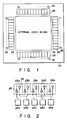
- Fig. 1 is a view showing chip layout of a conventional master slice type semiconductor integrated circuit.
- An internal logic block 22 is formed at the center of a chip body 21, and I/O cells 23 constituted by input and output buffers (not shown) are arranged in the peripheral portion at a predetermined pitch.
- a pad 24 is arranged for each I/O cell in a one-to-one correspondence. The pads 24 are arranged at the same pitch as the I/O cells.
- a wiring pattern is formed to connect the components within the internal logic block 22, between the internal logic block 22 and the I/O cells 23, and between the I/O cells 23 and the corresponding pads 24.
- Each pad 24 serves as an input or output pad, or an input/output pad.
- each pad is wire-bonded to a corresponding pin of an IC.
- a load drive capacity as well as areas of the respective I/O cells 23 are equal to each other in favor of easy cell design. For this reason, when a large load capacitor is driven, the drive capacity may be insufficient when only one I/O cell is used.
- output buffers in a plurality of I/O cells are connected in parallel with each other, as disclosed in Japanese Patent Disclosure (Kokai) No. 60-169150.
- reference numerals 23a to 23e denote I/O cells each including an input buffer 25 and an output buffer 26; and 24a to 24e, pads formed in one-to-one correspondence with the I/O cells 23a to 23e.
- the pads 24a, 24c, and 24d are connected to only the input buffers 25 in the I/O cells 23a, 23c, and 23d, respectively. In this case, these pads are used as the input pads.
- the pad 24b is connected in parallel with the output buffers 26 in the two I/O cells 23a and 23b.
- the pad 24b is used as an output pad having a load drive capacity twice that of an I/O cell.
- the pad 24e is connected in parallel with output buffers 26 in the three I/O cells 23c, 23d, and 23e.
- the pad 24e is used as an output pad having a load drive capacity three times that of an I/O cell.
- output buffers in a plurality of I/O cells are connected in parallel with each other at the time of formation of a wiring pattern. Therefore, the load drive capacity can be arbitrarily selected without changing the size of the chip body.
- the present invention has been made in consideration of the above situation, and has as its object to provide a master slice type semiconductor integrated circuit wherein I/O cells need not be designed again when pad pitches are changed, and a load drive capacity can be arbitrarily selected without changing the size of a chip body.
- a master slice type semiconductor integrated circuit comprising a plurality of pads arranged at a predetermined pitch and a number n , n being an integer of 2 or more, of I/O cells of equal area arranged for each of the plurality of pads, each I/O cell being provided with at least a buffer, wherein the number n of I/O cells per pad is set in accordance with the pad pitch.
- Fig. 3 is a view showing chip layout of a master slice type semiconductor integrated circuit according to an embodiment of the present invention.
- reference numeral 11 denotes a chip body; and 12, an internal logic block.
- a plurality of I/O cells 13 and a plurality of pads 14 are arranged in a peripheral portion of the chip body 11.
- three I/O cells 13 are arranged for each pad 14. That is, the number of I/O cells 13 is three times that of the pads 14 in the chip body 11.
- Fig. 4 is a plan view showing only an IC peripheral portion of the above embodiment.
- Reference numerals 13a to 13i denote I/O cells each including an input buffer 15 and an output buffer 16.
- Reference numerals 14a, 14b, and 14c denote pads, respectively.
- the three I/O cells 13a, 13b, and 13c are arranged for the pad 14a, the three I/O cells 13d, 13e, and 13f are arranged for the pad 14b, and the three I/O cells 13g, 13h, and 13i are arranged for the pad 14c.
- the input buffers 15 included in the respective I/O cells 13 have equal electrical characteristics.
- the output buffers 16 have equal electrical characteristics such as a load drive capacity.
- the respective I/O cells 13 have equal areas.
- each of the I/O cells 13a to 13i along its alignment direction is defined as, e.g., 50 ⁇ m, and the pads 14 are arranged at a pitch of 150 ⁇ m, as shown in Fig. 4.
- Fig. 5 shows a state wherein a wiring pattern is formed in the IC having the arrangement described above.
- the pad 14a is connected in parallel with the output buffers 16 of the I/O cells 13a and 13b.
- the pad 14a is used as an output pad having a load drive capacity twice that of an I/O cell.
- the pad 14b is connected in parallel with the input buffer 15 of the I/O cell 13c and the output buffers 16 of the I/O cells 13d, 13e, and 13f.
- the pad 14b serves as an input/output pad having a load drive capacity three times that of an I/O cell.
- the pad 14c is connected in parallel with the input buffer 15 of the I/O cell 13g and the output buffers 16 of the I/O cells 13h and 13i.
- the pad 14c serves as an output/input pad having a load drive capacity twice that of an I/O cell.
- a plurality of output buffers are connected in parallel with one output pad during formation of a wiring pattern. Therefore, the load drive capacity can be arbitrarily selected without changing the size of the chip body.
- a plurality of I/O cells is arranged for each pad.
- This arrangement is compatible with a change in pad pitch without redesigning the I/O cell.
- the pitch of the pads 14 is set to be 150 ⁇ m. If the pad pitch must be reduced to 100 ⁇ m, two I/O cells can be arranged for each pad. That is, as shown in Fig. 6, two I/O cells 13a and 13b are arranged for a pad 14a, two I/O cells 13c and 13d are arranged for a pad 14b, two I/O cells 13e and 13f are arranged for a pad 14c, and two I/O cells 13g and 13h are arranged for a pad 14d.
- the I/O cells 13 can be the same as those in Fig. 4. Therefore, I/O cells need not be designed again.
- the circuit arrangement in Fig. 6 can be manufactured by reducing only the number of I/O cells per pad as compared with the number of I/O cells in the IC of Fig. 4.
- a relative position between each pad 14 and the corresponding I/O cell 13 is kept unchanged. More specifically, the center of each pad 14 can always be aligned with that of the corresponding I/O cell 13, so that automatic computer-aided wiring can be performed to form a wiring pattern.
- each I/O cell of the above embodiment consists of one input buffer and one output buffer.
- the present invention is also applicable to a general I/O cell including for instance an input protective resistor or diode, or transistor.
- Fig. 7 shows an arrangement of an I/O cell 13 used in a practical IC before a wiring pattern is formed.
- a plurality of inverters 31 which constitute an input buffer and an output buffer and input protective resistors 32 are formed in the I/O cell 13.
- the I/O cells having different wiring patterns are shown in Figs. 8 and 9.
- the input terminals of all the inverters 31 are connected in parallel with each other, and their output terminals are also connected in parallel with each other to constitute an output buffer 16.
- the parallel-connected output terminals of the inverters 31 are simultaneously connected to a pad 14 during formation of a wiring pattern.
- a half of the input terminals and a half of the output terminals of the inverters 31 are connected in parallel with each other, respectively.
- the half of the inverters constitutes an input buffer 15, and the remaining half of the inverters constitutes an output buffer 16.
- the input terminals of the inverters 31 constituting the input buffer 15 are connected to a pad 14 through the input protective resistor 32, and the output terminals of the inverters 31 constituting the output buffer 16 are directly connected to the pad 14.
- the buffers of the plurality of I/O cells are connected in parallel with each other to select an arbitrary load drive capacity.
- the present invention can also cope with a change in pad pitch by reducing the number n of I/O cells arranged for each pad. As a result, the I/O cell need not be designed again at the time of a change in pad pitch. Therefore, the load drive capacity can be arbitrarily selected without changing the size of the chip body.
Landscapes
- Physics & Mathematics (AREA)
- Engineering & Computer Science (AREA)
- Computer Hardware Design (AREA)
- Computing Systems (AREA)
- General Engineering & Computer Science (AREA)
- Mathematical Physics (AREA)
- Design And Manufacture Of Integrated Circuits (AREA)
- Semiconductor Integrated Circuits (AREA)
- Logic Circuits (AREA)
Claims (3)
- Integrierte Standardscheiben-Halbleiterschaltung mit
einer Vielzahl in vorgegebenem Abstand angeordneter Anschlußinseln (14, 14a - 14d)
und einer Anzahl von n Ein-/Ausgangszellen (13, 13a - 13i) gleicher Fläche, die für jede der Anschlußinseln angeordnet sind und wobei jede Ein-/Ausgangszelle mit mindestens einem Puffer (15) versehen ist,
dadurch gekennzeichnet, daß
die Anzahl n der Ein-/Ausgangszellen (13, 13a - 13i) pro Anschlußpunkt (14, 14a - 14d) ganzzahlig, gleich oder größer als 2 und mit dem Abstand der Anschlußinseln in Übereinstimmung gebracht ist. - Schaltung nach Anspruch 1,
dadurch gekennzeichnet, daß
die in den Ein-/Ausgangszellen (13, 13a - 13i) enthaltenen Puffer (15) gleiche Treiberdurchlaßfähigkeit haben. - Schaltung nach Anspruch 1,
dadurch gekennzeichnet, daß
jede der Ein-/Ausgangszellen (13, 13a - 13i) zusätzlich zum Puffer einen Eingangsschutzwiderstand (32) enthält.
Applications Claiming Priority (2)
| Application Number | Priority Date | Filing Date | Title |
|---|---|---|---|
| JP118765/88 | 1988-05-16 | ||
| JP63118765A JPH01289138A (ja) | 1988-05-16 | 1988-05-16 | マスタースライス型半導体集積回路 |
Publications (3)
| Publication Number | Publication Date |
|---|---|
| EP0342590A2 EP0342590A2 (de) | 1989-11-23 |
| EP0342590A3 EP0342590A3 (de) | 1991-09-04 |
| EP0342590B1 true EP0342590B1 (de) | 1994-08-17 |
Family
ID=14744510
Family Applications (1)
| Application Number | Title | Priority Date | Filing Date |
|---|---|---|---|
| EP89108755A Expired - Lifetime EP0342590B1 (de) | 1988-05-16 | 1989-05-16 | Anordnung für integrierte Halbleiterschaltung vom Master-Slice Typ |
Country Status (5)
| Country | Link |
|---|---|
| US (1) | US4942317A (de) |
| EP (1) | EP0342590B1 (de) |
| JP (1) | JPH01289138A (de) |
| KR (1) | KR960006977B1 (de) |
| DE (1) | DE68917515T2 (de) |
Families Citing this family (18)
| Publication number | Priority date | Publication date | Assignee | Title |
|---|---|---|---|---|
| US6825698B2 (en) * | 2001-08-29 | 2004-11-30 | Altera Corporation | Programmable high speed I/O interface |
| JP2509696B2 (ja) * | 1989-04-26 | 1996-06-26 | 株式会社東芝 | ゲ―トアレ―半導体集積回路装置 |
| JPH03274765A (ja) * | 1990-03-23 | 1991-12-05 | Mitsubishi Electric Corp | マスタスライス方式半導体装置 |
| US5208764A (en) * | 1990-10-29 | 1993-05-04 | Sun Microsystems, Inc. | Method for optimizing automatic place and route layout for full scan circuits |
| JP2720629B2 (ja) * | 1991-04-26 | 1998-03-04 | 日本電気株式会社 | 集積回路のレイアウトシステム |
| WO1993012540A1 (en) * | 1991-12-10 | 1993-06-24 | Vlsi Technology, Inc. | Integrated circuit with variable pad pitch |
| KR960003042B1 (ko) * | 1992-05-26 | 1996-03-04 | 가부시끼가이샤 도시바 | 데이타 출력 장치 |
| US5535084A (en) * | 1992-07-24 | 1996-07-09 | Kawasaki Steel Corporation | Semiconductor integrated circuit having protection circuits |
| JPH06326194A (ja) * | 1993-05-17 | 1994-11-25 | Mitsubishi Electric Corp | 半導体集積回路装置 |
| US5469473A (en) * | 1994-04-15 | 1995-11-21 | Texas Instruments Incorporated | Transceiver circuit with transition detection |
| US6480817B1 (en) * | 1994-09-01 | 2002-11-12 | Hynix Semiconductor, Inc. | Integrated circuit I/O pad cell modeling |
| EP0743756B1 (de) * | 1995-05-05 | 1997-08-13 | Siemens Aktiengesellschaft | Konfigurierbare integrierte Schaltung |
| US5995740A (en) * | 1996-12-23 | 1999-11-30 | Lsi Logic Corporation | Method for capturing ASIC I/O pin data for tester compatibility analysis |
| US6157051A (en) * | 1998-07-10 | 2000-12-05 | Hilevel Technology, Inc. | Multiple function array based application specific integrated circuit |
| JP2002026130A (ja) * | 2000-07-06 | 2002-01-25 | Nec Microsystems Ltd | 半導体集積回路及びi/oブロック配置方法 |
| US7281227B2 (en) * | 2004-09-30 | 2007-10-09 | Infineon Technologies Ag | Method and device for the computer-aided design of a supply network |
| US8302060B2 (en) * | 2010-11-17 | 2012-10-30 | Taiwan Semiconductor Manufacturing Co., Ltd. | I/O cell architecture |
| WO2020073901A1 (en) * | 2018-10-11 | 2020-04-16 | Changxin Memory Technologies, Inc. | Semiconductor structure, memory device, semiconductor device and method of manufacturing the same |
Family Cites Families (15)
| Publication number | Priority date | Publication date | Assignee | Title |
|---|---|---|---|---|
| JPS57211248A (en) * | 1981-06-22 | 1982-12-25 | Hitachi Ltd | Semiconductor integrated circuit device |
| JPS5835963A (ja) * | 1981-08-28 | 1983-03-02 | Fujitsu Ltd | 集積回路装置 |
| EP0074805B2 (de) * | 1981-09-10 | 1992-03-11 | Fujitsu Limited | Integrierte Halbleiterschaltung mit einem Halbleitersubstrat und Verbindungsschichten |
| JPS593950A (ja) * | 1982-06-30 | 1984-01-10 | Fujitsu Ltd | ゲ−トアレイチツプ |
| JPS6027145A (ja) * | 1983-07-25 | 1985-02-12 | Hitachi Ltd | 半導体集積回路装置 |
| JPS6035532A (ja) * | 1983-07-29 | 1985-02-23 | Fujitsu Ltd | マスタスライス集積回路装置 |
| JPS6074644A (ja) * | 1983-09-30 | 1985-04-26 | Fujitsu Ltd | Cmosゲ−トアレ− |
| JP2564787B2 (ja) * | 1983-12-23 | 1996-12-18 | 富士通株式会社 | ゲートアレー大規模集積回路装置及びその製造方法 |
| JPS60169150A (ja) * | 1984-02-13 | 1985-09-02 | Hitachi Ltd | 集積回路 |
| JPS61100947A (ja) * | 1984-10-22 | 1986-05-19 | Toshiba Corp | 半導体集積回路装置 |
| JPS62285443A (ja) * | 1986-06-03 | 1987-12-11 | Fuji Photo Film Co Ltd | マスタスライス集積回路装置 |
| US4864381A (en) * | 1986-06-23 | 1989-09-05 | Harris Corporation | Hierarchical variable die size gate array architecture |
| JPH06105757B2 (ja) * | 1987-02-13 | 1994-12-21 | 富士通株式会社 | マスタ・スライス型半導体集積回路 |
| US4819047A (en) * | 1987-05-15 | 1989-04-04 | Advanced Micro Devices, Inc. | Protection system for CMOS integrated circuits |
| JP2566998B2 (ja) * | 1987-11-20 | 1996-12-25 | 株式会社日立製作所 | 半導体装置 |
-
1988
- 1988-05-16 JP JP63118765A patent/JPH01289138A/ja active Pending
-
1989
- 1989-05-12 US US07/351,001 patent/US4942317A/en not_active Expired - Lifetime
- 1989-05-16 KR KR1019890006518A patent/KR960006977B1/ko not_active Expired - Fee Related
- 1989-05-16 EP EP89108755A patent/EP0342590B1/de not_active Expired - Lifetime
- 1989-05-16 DE DE68917515T patent/DE68917515T2/de not_active Expired - Fee Related
Also Published As
| Publication number | Publication date |
|---|---|
| US4942317A (en) | 1990-07-17 |
| EP0342590A2 (de) | 1989-11-23 |
| DE68917515D1 (de) | 1994-09-22 |
| EP0342590A3 (de) | 1991-09-04 |
| JPH01289138A (ja) | 1989-11-21 |
| DE68917515T2 (de) | 1995-02-09 |
| KR890017794A (ko) | 1989-12-18 |
| KR960006977B1 (ko) | 1996-05-25 |
Similar Documents
| Publication | Publication Date | Title |
|---|---|---|
| EP0342590B1 (de) | Anordnung für integrierte Halbleiterschaltung vom Master-Slice Typ | |
| US5598347A (en) | Layout method for designing an integrated circuit device by using standard cells | |
| EP0257437A2 (de) | Integrierte Schaltung in Hauptscheibentechnik | |
| EP0563973B1 (de) | Integrierte Masterslice-Schaltung mit reduzierten Chipabmessungen und vermindertem Speisespannungsrauschen | |
| EP0278857B1 (de) | Integrierte Schaltung vom Typ "Masterslice" | |
| EP0074825B2 (de) | Herstellung von integrierten Schaltungen nach dem Mutterscheibenverfahren | |
| EP0612151B1 (de) | Halbleitervorrichtung zur Reduzierung einer Taktverschiebung in einer Vielfalt von Mustern von Verdrahtungsblöcken | |
| US4947233A (en) | Semi-custom LSI having input/output cells | |
| US5083181A (en) | Semiconductor integrated circuit device and wiring method thereof | |
| US5270592A (en) | Clock supply circuit layout in a circuit area | |
| EP0194205B1 (de) | Verfahren zum Herstellen eines Einzelchip-Mikrocomputers | |
| EP0453106B1 (de) | Zusammengesetzte elektrische Bauteile | |
| EP0021661A1 (de) | Masterslice-Halbleitervorrichtung | |
| US5206529A (en) | Semiconductor integrated circuit device | |
| US5952684A (en) | Chip layout of semiconductor integrated circuit | |
| US6013924A (en) | Semiconductor integrated circuit and method for making wiring layout of semiconductor integrated circuit | |
| EP0349294B1 (de) | I/O-Zellen für integrierte Halbleiterschaltungen | |
| JPH06101521B2 (ja) | 半導体集積回路装置 | |
| JPH02186668A (ja) | 集積回路装置 | |
| US4959555A (en) | Interconnection medium | |
| JPH01152642A (ja) | 半導体集積回路 | |
| EP0637083B1 (de) | Halbleiteranordnung mit geringem Flächenbedarf der Verbindungen innerhalb und ausserhalb des Datenleitungsgebietes | |
| JPS6366059B2 (de) | ||
| JPH02306650A (ja) | 半導体装置 | |
| JPS6364054B2 (de) |
Legal Events
| Date | Code | Title | Description |
|---|---|---|---|
| PUAI | Public reference made under article 153(3) epc to a published international application that has entered the european phase |
Free format text: ORIGINAL CODE: 0009012 |
|
| 17P | Request for examination filed |
Effective date: 19890516 |
|
| AK | Designated contracting states |
Kind code of ref document: A2 Designated state(s): DE FR GB IT |
|
| PUAL | Search report despatched |
Free format text: ORIGINAL CODE: 0009013 |
|
| RHK1 | Main classification (correction) |
Ipc: H01L 23/50 |
|
| AK | Designated contracting states |
Kind code of ref document: A3 Designated state(s): DE FR GB IT |
|
| 17Q | First examination report despatched |
Effective date: 19930319 |
|
| GRAA | (expected) grant |
Free format text: ORIGINAL CODE: 0009210 |
|
| AK | Designated contracting states |
Kind code of ref document: B1 Designated state(s): DE FR GB IT |
|
| PG25 | Lapsed in a contracting state [announced via postgrant information from national office to epo] |
Ref country code: IT Free format text: LAPSE BECAUSE OF FAILURE TO SUBMIT A TRANSLATION OF THE DESCRIPTION OR TO PAY THE FEE WITHIN THE PRE;WARNING: LAPSES OF ITALIAN PATENTS WITH EFFECTIVE DATE BEFORE 2007 MAY HAVE OCCURRED AT ANY TIME BEFORE 2007. THE CORRECT EFFECTIVE DATE MAY BE DIFFERENT FROM THE ONE RECORDED.SCRIBED TIME-LIMIT Effective date: 19940817 |
|
| REF | Corresponds to: |
Ref document number: 68917515 Country of ref document: DE Date of ref document: 19940922 |
|
| ET | Fr: translation filed | ||
| PLBE | No opposition filed within time limit |
Free format text: ORIGINAL CODE: 0009261 |
|
| STAA | Information on the status of an ep patent application or granted ep patent |
Free format text: STATUS: NO OPPOSITION FILED WITHIN TIME LIMIT |
|
| 26N | No opposition filed | ||
| REG | Reference to a national code |
Ref country code: GB Ref legal event code: IF02 |
|
| PGFP | Annual fee paid to national office [announced via postgrant information from national office to epo] |
Ref country code: DE Payment date: 20070510 Year of fee payment: 19 |
|
| PGFP | Annual fee paid to national office [announced via postgrant information from national office to epo] |
Ref country code: GB Payment date: 20070516 Year of fee payment: 19 |
|
| PGFP | Annual fee paid to national office [announced via postgrant information from national office to epo] |
Ref country code: FR Payment date: 20070510 Year of fee payment: 19 |
|
| GBPC | Gb: european patent ceased through non-payment of renewal fee |
Effective date: 20080516 |
|
| REG | Reference to a national code |
Ref country code: FR Ref legal event code: ST Effective date: 20090119 |
|
| PG25 | Lapsed in a contracting state [announced via postgrant information from national office to epo] |
Ref country code: DE Free format text: LAPSE BECAUSE OF NON-PAYMENT OF DUE FEES Effective date: 20081202 Ref country code: FR Free format text: LAPSE BECAUSE OF NON-PAYMENT OF DUE FEES Effective date: 20080602 |
|
| PG25 | Lapsed in a contracting state [announced via postgrant information from national office to epo] |
Ref country code: GB Free format text: LAPSE BECAUSE OF NON-PAYMENT OF DUE FEES Effective date: 20080516 |