EP0342511A2 - Aporturkorrekturschaltung - Google Patents
Aporturkorrekturschaltung Download PDFInfo
- Publication number
- EP0342511A2 EP0342511A2 EP89108431A EP89108431A EP0342511A2 EP 0342511 A2 EP0342511 A2 EP 0342511A2 EP 89108431 A EP89108431 A EP 89108431A EP 89108431 A EP89108431 A EP 89108431A EP 0342511 A2 EP0342511 A2 EP 0342511A2
- Authority
- EP
- European Patent Office
- Prior art keywords
- signal
- shoot
- preshoot
- overshoot
- aperture correction
- Prior art date
- Legal status (The legal status is an assumption and is not a legal conclusion. Google has not performed a legal analysis and makes no representation as to the accuracy of the status listed.)
- Granted
Links
Images


Classifications
-
- H—ELECTRICITY
- H04—ELECTRIC COMMUNICATION TECHNIQUE
- H04N—PICTORIAL COMMUNICATION, e.g. TELEVISION
- H04N5/00—Details of television systems
- H04N5/14—Picture signal circuitry for video frequency region
- H04N5/20—Circuitry for controlling amplitude response
- H04N5/205—Circuitry for controlling amplitude response for correcting amplitude versus frequency characteristic
- H04N5/208—Circuitry for controlling amplitude response for correcting amplitude versus frequency characteristic for compensating for attenuation of high frequency components, e.g. crispening, aperture distortion correction
Definitions
- the present invention relates to an aperture correction circuit which corrects the aperture aberration of the video signal of a television receiver in order to reproduce a sharp image.
- Fig. 4 is a block diagram showing the circuit arrangement of the prior-art example, while Figs. 5A - 5F are waveform diagrams of the signals of various portions within the circuit shown in Fig. 4.
- a signal S0 when a signal S0 is received at a video signal input terminal 1, a signal S1 delayed through a delay circuit 2 and a signal S2 further delayed through a delay circuit 3 are obtained.
- the signals S0 and S2 are added by an adder 43 to produce a signal S A . Since this signal S A becomes a signal as indicated by S A in Fig. 5D, an aperture correcting shoot signal S B (shown in Fig. 5E) can be obtained in such a way that the signal S1 being the output of the delay circuit 2 is subtracted from the signal S A by a subtracter 44.
- the ratio between the amplitudes of a preshoot signal (a) and an overshoot signal (b) has generally been 1 : 1 with the prior-art circuit arrangement.
- the amplitude ratio between the preshoot signal and the overshoot signal can be set as being somewhat unbalanced. Since, however, the balance between the amplitude ratio of the shoot signals is fixed to the last, the prior-art system has been difficult of attaining image qualities in correspondence with various video input sources or input conditions.
- a signal S0 received at a video signal input terminal 1 is applied to a delayed video signal terminal 51 for a video chroma IC 60 (in Fig. 6, only a video circuit is shown in blocks) through a delay line 2.
- the signal S0 is further applied to a video signal input terminal 50 from the input side of the delay line 2.
- the applied signals are subjected to reflection-type delay-line aperture correction processing by an image quality adjuster 56, thereby to compose a shoot signal.
- the amount of the shoot signal to be superposed on the video signal is varied according to a control signal at an image quality adjusting input terminal 52, whereby the image quality of the video signal is adjusted.
- the resulting output SA is delivered to a luminance signal output terminal 68 for the IC 60 via a contrast adjuster 57, a pedestal clamp circuit 58 and a luminance signal amplifier 59.
- the output of the terminal 68 is amplified by an emitter follower of Darlington connection which is configured of an N-P-N transistor 71, a P-N-P transistor 72, and resistors 70, 73.
- the amplified output signal is delivered from a luminance signal output terminal 75 to a CRT drive circuit at a succeeding stage.
- the amplified output signal is passed via a resistor 69 and is further amplified by an emitter follower circuit which is configured of a P-N-P transistor 67 and a resistor 66.
- the resulting output is divided by resistors 61, 63 and a variable resistor 62, and the divided voltage is applied as the control signal to the image quality adjusting input terminal 52.
- the image quality namely, the amount of the shoot signal to be added to the original signal of the video signal is controlled according to the output amplitude of the output luminance signal, thereby to make the corrections of decreasing the amount of the shoot signal at a bright part on a picture frame so as to relieve blooming and increasing the amount of the shoot signal at a dark part.
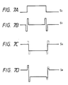
- the signal waveforms at several parts in the arrangement become as illustrated in Figs. 7A - 7D.
- the original signal S0 of the video signal (in Fig. 7A) and the shoot signal S S composed from the signal S0 (in Fig. 7B) are added by the image quality adjuster 56 in Fig. 6, to become as indicated by dotted lines at S A (in Fig. 7C).
- the signal waveform at the luminance signal output terminal 68 in Fig. 6, and the waveform S B (in Fig. 7D) at the emitter follower output 75 in Fig. 6 become waveforms of dotted lines accordingly. Since, however, the waveform S B (in Fig.
- the timing of the composition of the video signal and the aperture correction signal is not sufficiently considered, either, so that the image quality adjustment at the leading edge of the aperture has been unsatisfactory.
- An object of the present invention is to provide an aperture correction circuit for images which permits all video inputs to undergo aperture corrections of optimal conditions, whereby a picture frame can be reproduced under the optimal conditions.
- Another object of the present invention is to realize optimal aperture corrections of proper timings in accordance with signal contents, whereby a picture frame is reproduced under optimal conditions.
- the aperture correction circuit of the present invention comprises a preshoot signal generator which generates the preshoot signal of the edge part of a video signal, an overshoot signal generator which generates the overshoot signal of the edge part of the video signal, a shoot signal composition circuit which adds the preshoot signal and the overshoot signal at an addition ratio corresponding to a control signal, thereby to deliver the resulting signal as a correcting shoot signal, and an adder which adds the video signal and the correcting shoot signal, thereby to deliver the resulting signal as an output.
- the ratio between the amplitude of the preshoot signal and that of the overshoot signal changes according to the control signal, so that an image quality can be adjusted according to the input signal by dynamically changing the control signal in accordance with the input signal.
- the differentiated signal of the input video signal is employed as the control signal.
- Fig. 1 is a block diagram showing the fundamental arrangement of an embodiment of the present invention
- Figs. 2A - 2C are waveform diagrams each showing the signals of various parts in Fig. 1
- Fig. 3 is a circuit diagram showing an example of the practicable circuit of an essential portion in Fig. 1.
- a signal S0 received at a video signal input terminal 1 are passed through a delay circuit 2 and a delay circuit 3 to be respectively delivered as delayed signals S1 and S2.
- a subtracter 4 subtracts the input signal S0 from the output S1 of the delay circuit 2, thereby to deliver a preshoot signal S3 as an output.
- a subtracter 5 subtracts the output S2 of the delay circuit 3 from the output S1 of the delay circuit 2, thereby to deliver an overshoot signal S4 as an output.
- the preshoot signal S3 and the overshoot signal S4 are respectively applied to variable-gain amplifiers 9 and 8, and they are amplified into gain control characteristics reverse to each other by a gain control circuit 7 which controls the gains of the amplifiers 8 and 9 in accordance with a control input from a shoot-balance control input terminal 6. Accordingly, the ratio between the outputs of the respective amplifiers, namely, the ratio between the amplitudes of a preshoot signal S3′ and an overshoot signal S4′ is set according to the gain control signal.
- the output signals S3′ and S4′ are added by an adder 10, thereby to become a composite shoot signal S5.
- the composite shoot signal S5 becomes one in which the ratio of the amplitudes of the preshoot signal and the overshoot signal has been controlled according to the shoot-balance control input 6.
- the composite shoot signal S5 is amplified by an amplifier 11, the output S6 of which and the output signal S1 of the delay circuit 2 are added by an adder 12, whereby a video signal S7 after aperture corrections is delivered to an output terminal 13.
- a portion enclosed with a dotted line in the figure, namely, a portion including the gain control circuit 7 and the variable-gain amplifiers 8, 9 is a shoot-balance controller 14, by which the shoot balance of the preshoot and overshoot signals having hitherto been fixed can be rendered variable at will by the use of the single control input.
- the versatility of the aperture corrections increases to realize the setting of the shoot balance suited to an input source.
- Figs. 2A - 2C are the waveform diagrams each exemplifying the signals S0 - S7 of the various parts in Fig. 1.
- Fig. 2A corresponds to the state in which the amplitude of the preshoot signal and that of the overshoot signal are balanced
- Fig. 2B corresponds to the case of making the overshoot signal greater and the preshoot signal smaller by the use of the signal input of the control input terminal 6
- Fig. 2C corresponds to the case of making the preshoot signal greater and the overshoot signal smaller by the use of the signal input of the control input terminal 6.
- the signals down to the input signals S3 and S4 of the respective amplifiers 9 and 8 are identical in all the cases of Figs. 2A - 2C, and the balances of the shoot signals differ behind the variable-gain amplifiers 8 and 9.
- the amplitude of the composite shoot signal S5 (the preshoot signal + the overshoot signal) can also be held constant, depending upon the way of selecting the gain control characteristics of the variable-gain amplifiers.
- Fig. 3 is the circuit diagram showing the practicable example of the essential portion of the circuit depicted in Fig. 1.
- a circuit portion M enclosed with a broken (dotted) line in Fig. 3 practicable example of the circuit portion which includes the dotted-line portion shown in Fig. 1, namely, the shoot-balance controller 14, and the subtracters 4 and 5.
- the subtracter 4 for producing the preshoot signal is configured of N-P-N transistors 27, 28, a resistor 25, and current sources 18, 19; the gain thereof is controlled by N-P-N transistors 31 and 32; and the preshoot signal output appears at an output terminal 42 which leads to the line of the emitter of an N-P-N transistro 40.
- the subtracter 5 for producing the overshoot signal is configured of N-P-N transistors 30, 29, a resistor 26, and current sources 20, 21; the gain thereof is controlled by N-P-N transistors 37 and 38; and the overshoot signal output appears at the output terminal 42 which leads to the emitter line of the N-P-N transistor 40. Accordingly, the signal composed of the preshoot signal and the overshoot signal is obtained at the output terminal 42. Besides, in this example, the output signals of an output terminal 41 and the output terminal 42 are inverted outputs.
- the gain control is performed by the gain control circuit 7 configured of a constant-voltage source 17 and resistors 22, 23 and 24, using a variable-voltage source 43 connected to the shoot-balance control input terminal 6.
- the shunting ratio between the N-P-N transistors 31 and 32 for controlling the gain of the preshoot signal and the shunting ratio between the N-P-N transistors 37 and 38 for controlling the gain of the overshoot signal are controlled in reverse directions, whereby the sum between the amplitudes of the preshoot signal output and the overshoot signal output is held constant even when the shoot balance is changed.
- An N-P-N transistor 39 and the N-P-N transistor 40 which are the loads of the shoot outputs can also be replaced with resistors.
- the shoot balance between the preshoot signal and the overshoot signal can be freely set owing to the control input, and it can also be varied while the sum of the output amplitudes of the preshoot and overshoot signals is held constant.
- a signal S0 received at a video signal input terminal 1 is applied to an aperture correction signal generator 83 which is configured of a delay circuit 87 and a shoot signal composing circuit of variable shoot balance type 88, and to a differentiator 84.
- the output S c of the differentiator 84 is applied to the shoot-balance control input terminal 82 of the shoot-balance signal composing circuit 88.
- the shoot balance between shoot signals prepared from the input signal S0 is controlled by the variable shoot-balance type shoot signal composing circuit 88, and a composite shoot signal S b is derived from a composite shoot signal output terminal 81.
- an example of the portion 83 enclosed with a broken line in Fig. 8 can be configured, as shown in Fig. 9, of two delay circuits 87, 89, two subtracters 90, 91, two amplifiers 92, 93 whose gains are controlled in reverse directions by a gain controller 94, an adder 95, and an amplifier 96. These constituents are the same as in the circuit arrangement of Fig. 1.
- Fig. 8 The operation of the embodiment in Fig. 8 will be described with reference to Figs. 11A - 11G as to a case where the variable shoot-balance type shoot signal composing circuit 88 has control characteristics shown in Fig. 10 according to which, the ratio of a preshoot signal PS to an overshoot signal OS increases as the control voltage of the shoot-balance control input terminal 82 is raised, whereas the ratio of the overshoot signal OS increases as the control voltage is lowered.
- the input signal S0 has a waveform depicted in Fig. 11A
- the output S c of the differentiator 84 shown in Fig. 8 becomes a waveform depicted in Fig. 11C.
- the composite shoot signal output S b has a waveform depicted in Fig. 11D, namely, a waveform in which the preshoot signal and the overshoot signal are balanced, and let's consider a case where the output S c is applied to the control input terminal 82. Then, the signal S b comes to have a waveform as shown in Fig. 11E, namely, a shoot waveform in which a shoot for a black level is great and a shoot for a white level is small on each of the rise side and fall side of the input signal S0 and the rise and fall of which are substantially symmetric.
- the shoot balance is not controlled by the differentiated signal S c ,whereby the signal which suppresses blooming ascribable to the shoot for the white level and in which the shoots for the white level and the shoots for the black level are substantially symmetric to each other can be obtained without spoiling the sharpness of an aperture part.
- the differentiated signal S c since the differentiated signal S c has its signal level determined in proportion to the amplitude of the input signal S0 ,the amount of the unbalance of the shoot signals becomes small for the small amplitude of the signal S0 ,and it becomes large for the large amplitude.
- Fig. 12 is a diagram showing the fundamental arrangement of the third embodiment of the present invention.
- the signal S d at the aperture-corrected video output terminal 86 is applied to a luminance signal amplifier 100, and the output voltage of a variable-voltage source 101 is applied to a contrast control input terminal 99, whereby the gain of the amplifier 100 is controlled, and a luminance signal is delivered to a luminance signal output terminal 102.
- the luminance signal amplifier 100 is built in a video chroma IC in the case of a television receiver, and the signal of the output terminal 102 is applied to a CRT.
- a gain-controlled amplifier 97 is added between the differentiator 84 and the shoot-balance control input terminal 82 in Fig. 8, and the control input 98 thereof is supplied with the output of the contrast controlling variable- voltage source 101 stated above.
- the signal level of the differentiated signal S c to be applied to the shoot-balance control input 82 can be controlled in proportion to the level of the luminance signal which is applied from the luminance signal output terminal 102 to the CRT, so that the amount of the shoot for the white level on a picture frame can be optimalized.
- the aperture correcting adder 85 is usually set as an image quality adjuster and is often capable of varying the amounts of the shoot signals to-be-added in accordance with a control voltage.
- Fig. 13 is a diagram showing the fundamental arrangement of the fourth embodiment of the present invention.
- the input signal S0 is converted into a digital signal S0′ by an A/D (analog-to-digital) converter 103, and the same processing as in Fig. 8 is thereafter performed by digital signal processing, whereby effects similar to those of the embodiment in Fig. 8 are achieved.
- A/D analog-to-digital
- Fig. 14 is a diagram showing the fundamental arrangement of the fifth embodiment of the present invention.
- the input signal S0 is converted into the digital signal S0′ by the A/D converter 103 as in Fig. 13, and the same processing as in Fig. 12 is thereafter performed by digital signal processing in the same way as in Fig. 12 that the differentiated signal level for controlling the shoot balance is interlocked with the contrast control. Therefore, a more optimalized aperture-corrected picture frame can be reproduced.
- the operation of the embodiment in Fig. 13 will be described with reference to Figs. 15A - 15D and Figs. 11A - 11G.
- the signal waveforms of various parts shall be explained as being converted into analog signals.
- aperture corrections are made without using the luminance signal at the posterior stage, so that the time delay of the aperture part as in the prior-art system is not involved.
- a control signal and an aperture correction signal are obtained from an identical input signal in contrast to the prior-art system in which the aperture corrections of a present-time signal are made by the use of a luminance signal at a final stage, namely, a past signal. Therefore, aperture corrections can be made at the optimal timing, and the amounts of shoot signals for a white level and those of shoot signals for a black level can be rendered symmetric at the rise (black level ⁇ white level) part and fall (white level ⁇ black level) part of the signal. Moreover, since the amount of the shoot signal for the white level is proportional to the level of the video input signal, the invention is effective to suppress the peak level of the shoot signal for the white level, which brings forth the effect that blooming on a CRT can be relieved.
- the present invention is also applicable to digital television, and can be adopted irrespective of analog and digital systems.
- the differentiated signal for controlling the shoot balance can also be produced in such a way that the delay circuits in the shoot signal composing circuit (Fig. 3) are utilized, and that the input of the delay circuit 136 is subtracted from the output of the delay circuit 138. In this case, a portion including a subtracter 152 as enclosed with a broken line constructs a differentiator.
- the operation of the circuit arrangement in Fig. 16 will be described with reference to Figs. 17A - 17G similar to Figs. 11A - 11G.
- a composite shoot signal output S2 becomes a waveform as shown in Fig. 17E, and this waveform is one of good symmetry in which the peak of each shoot signal does not have a slope ascribable to the differentiated signal, in contrast to the case illustrated in Fig. 11E. Therefore, when the signal S2 in Fig. 17E is added with a main signal S1 shown in Fig. 17B, an aperture correction output S4 becomes as shown in Fig. 17G, and the waveform thereof is more improved over the signal S d in Fig. 11G.
Landscapes
- Engineering & Computer Science (AREA)
- Multimedia (AREA)
- Signal Processing (AREA)
- Picture Signal Circuits (AREA)
Applications Claiming Priority (4)
| Application Number | Priority Date | Filing Date | Title |
|---|---|---|---|
| JP11909388 | 1988-05-18 | ||
| JP119093/88 | 1988-05-18 | ||
| JP22236188 | 1988-09-07 | ||
| JP222361/88 | 1988-09-07 |
Publications (3)
| Publication Number | Publication Date |
|---|---|
| EP0342511A2 true EP0342511A2 (de) | 1989-11-23 |
| EP0342511A3 EP0342511A3 (en) | 1990-07-25 |
| EP0342511B1 EP0342511B1 (de) | 1995-05-03 |
Family
ID=26456891
Family Applications (1)
| Application Number | Title | Priority Date | Filing Date |
|---|---|---|---|
| EP89108431A Expired - Lifetime EP0342511B1 (de) | 1988-05-18 | 1989-05-10 | Aporturkorrekturschaltung |
Country Status (4)
| Country | Link |
|---|---|
| US (1) | US4994915A (de) |
| EP (1) | EP0342511B1 (de) |
| JP (1) | JP2865705B2 (de) |
| DE (1) | DE68922433T2 (de) |
Cited By (6)
| Publication number | Priority date | Publication date | Assignee | Title |
|---|---|---|---|---|
| EP0421369A3 (en) * | 1989-10-04 | 1991-11-06 | Sony Corporation | Color signal processing apparatus |
| EP0560170A3 (de) * | 1992-03-09 | 1994-01-05 | Thomson Consumer Electronics | |
| EP0840501A1 (de) * | 1996-10-29 | 1998-05-06 | Daewoo Electronics Co., Ltd | Schaltung zur Vergrösserung der Schärfe eines Videosignals |
| EP0982936A1 (de) * | 1998-08-28 | 2000-03-01 | Alps Electric Co., Ltd. | Konturkorrekturschaltung für eine Bildanzeigevorrichtung |
| EP1580474A1 (de) | 2004-03-25 | 2005-09-28 | MANIFATTURA TUBI GOMMA S.p.A. | Mehrschichtiger, flexibler Schlauch |
| DE19513613B4 (de) * | 1994-04-15 | 2007-04-05 | Matsushita Electric Industrial Co., Ltd., Kadoma | Horizontal-Konturverstärkungssignalprozessor |
Families Citing this family (16)
| Publication number | Priority date | Publication date | Assignee | Title |
|---|---|---|---|---|
| US5343244A (en) * | 1989-10-18 | 1994-08-30 | Sony Corporation | Video signal processing apparatus for use with a video camera |
| DE69123780T2 (de) * | 1990-04-27 | 1997-05-07 | Canon Kk | Gerät zur Verarbeitung von Bildsignalen zwecks Verbesserung der Kantensteilheit |
| JP2551205B2 (ja) * | 1990-06-28 | 1996-11-06 | 日本ビクター株式会社 | 輪郭補正回路 |
| US5134482A (en) * | 1990-11-26 | 1992-07-28 | North American Philips Corporation | Adjustable video sharpness circuit |
| JP2852390B2 (ja) * | 1991-02-16 | 1999-02-03 | 株式会社半導体エネルギー研究所 | 表示装置 |
| KR950000326B1 (ko) * | 1991-12-27 | 1995-01-13 | 삼성전자 주식회사 | 윤곽보정장치 |
| US5546135A (en) * | 1992-02-28 | 1996-08-13 | Matsushita Electric Industrial Co., Ltd. | Contour restoration apparatus |
| US5903316A (en) * | 1992-12-25 | 1999-05-11 | Canon Kabushiki Kaisha | Information signal processing apparatus |
| US5615019A (en) * | 1994-04-21 | 1997-03-25 | Hitachi, Ltd. | Television apparatus with built-in optical disk device |
| JP3480615B2 (ja) * | 1994-12-28 | 2003-12-22 | ソニー株式会社 | 映像信号処理装置 |
| JPH09244609A (ja) * | 1996-03-06 | 1997-09-19 | Matsushita Electric Ind Co Ltd | 映像表示装置 |
| WO1998009443A1 (en) * | 1996-08-26 | 1998-03-05 | Philips Electronics N.V. | Sharpness control |
| GB2423660B (en) | 2005-02-25 | 2010-08-18 | Imagination Tech Ltd | A method and apparatus for controlling overshoot in a video enhancement system |
| US20080229370A1 (en) * | 2007-03-13 | 2008-09-18 | Zustak Frederick J | TV-centric system |
| JP5272697B2 (ja) * | 2008-12-15 | 2013-08-28 | ソニー株式会社 | 表示装置、表示データ処理装置、表示データ処理方法 |
| JP5742874B2 (ja) * | 2013-05-14 | 2015-07-01 | ソニー株式会社 | 表示装置 |
Family Cites Families (5)
| Publication number | Priority date | Publication date | Assignee | Title |
|---|---|---|---|---|
| NL158987B (nl) * | 1972-06-10 | 1978-12-15 | Philips Nv | Apertuurcorrector voor een televisiebeeldsignaal, alsmede televisie-opneeminrichting, daarvan voorzien. |
| JPS5068416A (de) * | 1973-10-19 | 1975-06-07 | ||
| US4041531A (en) * | 1974-07-05 | 1977-08-09 | Rca Corporation | Television signal processing apparatus including a transversal equalizer |
| JPS53146310A (en) * | 1977-05-26 | 1978-12-20 | Coors Container Co | Method of and apparatus for producing vessels for containing pressurized materials |
| JPS5668073A (en) * | 1979-11-07 | 1981-06-08 | Canon Inc | Outline correcting device of video signal |
-
1989
- 1989-05-10 EP EP89108431A patent/EP0342511B1/de not_active Expired - Lifetime
- 1989-05-10 US US07/349,869 patent/US4994915A/en not_active Expired - Lifetime
- 1989-05-10 DE DE68922433T patent/DE68922433T2/de not_active Expired - Fee Related
- 1989-05-15 JP JP1118578A patent/JP2865705B2/ja not_active Expired - Lifetime
Cited By (8)
| Publication number | Priority date | Publication date | Assignee | Title |
|---|---|---|---|---|
| EP0421369A3 (en) * | 1989-10-04 | 1991-11-06 | Sony Corporation | Color signal processing apparatus |
| US5159442A (en) * | 1989-10-04 | 1992-10-27 | Sony Corporation | Color signal processing apparatus |
| EP0560170A3 (de) * | 1992-03-09 | 1994-01-05 | Thomson Consumer Electronics | |
| DE19513613B4 (de) * | 1994-04-15 | 2007-04-05 | Matsushita Electric Industrial Co., Ltd., Kadoma | Horizontal-Konturverstärkungssignalprozessor |
| EP0840501A1 (de) * | 1996-10-29 | 1998-05-06 | Daewoo Electronics Co., Ltd | Schaltung zur Vergrösserung der Schärfe eines Videosignals |
| US5847774A (en) * | 1996-10-29 | 1998-12-08 | Daewoo Electronics Co., Ltd. | Video signal peaking circuit |
| EP0982936A1 (de) * | 1998-08-28 | 2000-03-01 | Alps Electric Co., Ltd. | Konturkorrekturschaltung für eine Bildanzeigevorrichtung |
| EP1580474A1 (de) | 2004-03-25 | 2005-09-28 | MANIFATTURA TUBI GOMMA S.p.A. | Mehrschichtiger, flexibler Schlauch |
Also Published As
| Publication number | Publication date |
|---|---|
| JP2865705B2 (ja) | 1999-03-08 |
| JPH02168776A (ja) | 1990-06-28 |
| EP0342511A3 (en) | 1990-07-25 |
| DE68922433D1 (de) | 1995-06-08 |
| DE68922433T2 (de) | 1996-01-11 |
| EP0342511B1 (de) | 1995-05-03 |
| US4994915A (en) | 1991-02-19 |
Similar Documents
| Publication | Publication Date | Title |
|---|---|---|
| EP0342511B1 (de) | Aporturkorrekturschaltung | |
| US5422680A (en) | Non-linear contrast control apparatus with pixel distribution measurement for video display system | |
| US5142354A (en) | Signal level correction circuit for a video signal | |
| JP2612508B2 (ja) | テレビジョン・システム用制御信号発生器 | |
| US5255080A (en) | Contrast corrector for video signal | |
| EP0729273A2 (de) | Vorrichtung zum Erzeugen einer Kompensationsspannung für eine Mehrfachbildwiedergabe und Video-Anzeige-Einrichtung zum Verwenden einer solchen Vorrichtung | |
| JPH07336718A (ja) | 映像表示装置 | |
| US5386231A (en) | Video camera | |
| JP2583325B2 (ja) | 階調補正回路 | |
| US6628222B2 (en) | Image processing apparatus having A/D converter | |
| KR950001442B1 (ko) | 윤곽 보정 회로 | |
| JP2661036B2 (ja) | 輪郭補正装置 | |
| JPH10145642A (ja) | 輪郭補償回路 | |
| US5684533A (en) | Color video camera capable of improving gradation of dark signal level | |
| JP2002044679A (ja) | 映像信号処理回路 | |
| JP2538366B2 (ja) | ビデオト―ン回路 | |
| JPH11284880A (ja) | 撮像装置 | |
| JPH10304394A (ja) | カラー受像管のビーム電流監視回路 | |
| JP2578591B2 (ja) | 自動利得制御回路 | |
| JP2874182B2 (ja) | 輝度調節装置 | |
| JP2970175B2 (ja) | ホワイトバランス制御装置 | |
| KR920008996Y1 (ko) | 휘도펄스 부가방식에 의한 휘도제어회로 | |
| JPH081544B2 (ja) | 表示装置 | |
| JPH05199533A (ja) | 受像管のガンマ補正システム,ガンマ補正回路及びガンマ掛算器 | |
| JPH0537949A (ja) | 画像信号処理装置 |
Legal Events
| Date | Code | Title | Description |
|---|---|---|---|
| PUAI | Public reference made under article 153(3) epc to a published international application that has entered the european phase |
Free format text: ORIGINAL CODE: 0009012 |
|
| 17P | Request for examination filed |
Effective date: 19890510 |
|
| AK | Designated contracting states |
Kind code of ref document: A2 Designated state(s): DE GB |
|
| PUAL | Search report despatched |
Free format text: ORIGINAL CODE: 0009013 |
|
| AK | Designated contracting states |
Kind code of ref document: A3 Designated state(s): DE GB |
|
| 17Q | First examination report despatched |
Effective date: 19930421 |
|
| GRAA | (expected) grant |
Free format text: ORIGINAL CODE: 0009210 |
|
| AK | Designated contracting states |
Kind code of ref document: B1 Designated state(s): DE GB |
|
| REF | Corresponds to: |
Ref document number: 68922433 Country of ref document: DE Date of ref document: 19950608 |
|
| PLBE | No opposition filed within time limit |
Free format text: ORIGINAL CODE: 0009261 |
|
| STAA | Information on the status of an ep patent application or granted ep patent |
Free format text: STATUS: NO OPPOSITION FILED WITHIN TIME LIMIT |
|
| 26N | No opposition filed | ||
| PGFP | Annual fee paid to national office [announced via postgrant information from national office to epo] |
Ref country code: GB Payment date: 19980430 Year of fee payment: 10 |
|
| PGFP | Annual fee paid to national office [announced via postgrant information from national office to epo] |
Ref country code: DE Payment date: 19980629 Year of fee payment: 10 |
|
| PG25 | Lapsed in a contracting state [announced via postgrant information from national office to epo] |
Ref country code: GB Free format text: LAPSE BECAUSE OF NON-PAYMENT OF DUE FEES Effective date: 19990510 |
|
| GBPC | Gb: european patent ceased through non-payment of renewal fee |
Effective date: 19990510 |
|
| PG25 | Lapsed in a contracting state [announced via postgrant information from national office to epo] |
Ref country code: DE Free format text: LAPSE BECAUSE OF NON-PAYMENT OF DUE FEES Effective date: 20000301 |