EP0336570B1 - Ansteuerverfahren für eine Anzeigevorrichtung - Google Patents
Ansteuerverfahren für eine Anzeigevorrichtung Download PDFInfo
- Publication number
- EP0336570B1 EP0336570B1 EP89302407A EP89302407A EP0336570B1 EP 0336570 B1 EP0336570 B1 EP 0336570B1 EP 89302407 A EP89302407 A EP 89302407A EP 89302407 A EP89302407 A EP 89302407A EP 0336570 B1 EP0336570 B1 EP 0336570B1
- Authority
- EP
- European Patent Office
- Prior art keywords
- display device
- modulation signals
- driving
- potential
- electrodes
- Prior art date
- Legal status (The legal status is an assumption and is not a legal conclusion. Google has not performed a legal analysis and makes no representation as to the accuracy of the status listed.)
- Expired - Lifetime
Links
Images





Classifications
-
- G—PHYSICS
- G09—EDUCATION; CRYPTOGRAPHY; DISPLAY; ADVERTISING; SEALS
- G09G—ARRANGEMENTS OR CIRCUITS FOR CONTROL OF INDICATING DEVICES USING STATIC MEANS TO PRESENT VARIABLE INFORMATION
- G09G3/00—Control arrangements or circuits, of interest only in connection with visual indicators other than cathode-ray tubes
- G09G3/20—Control arrangements or circuits, of interest only in connection with visual indicators other than cathode-ray tubes for presentation of an assembly of a number of characters, e.g. a page, by composing the assembly by combination of individual elements arranged in a matrix no fixed position being assigned to or needed to be assigned to the individual characters or partial characters
- G09G3/34—Control arrangements or circuits, of interest only in connection with visual indicators other than cathode-ray tubes for presentation of an assembly of a number of characters, e.g. a page, by composing the assembly by combination of individual elements arranged in a matrix no fixed position being assigned to or needed to be assigned to the individual characters or partial characters by control of light from an independent source
- G09G3/36—Control arrangements or circuits, of interest only in connection with visual indicators other than cathode-ray tubes for presentation of an assembly of a number of characters, e.g. a page, by composing the assembly by combination of individual elements arranged in a matrix no fixed position being assigned to or needed to be assigned to the individual characters or partial characters by control of light from an independent source using liquid crystals
- G09G3/3611—Control of matrices with row and column drivers
- G09G3/3648—Control of matrices with row and column drivers using an active matrix
- G09G3/3655—Details of drivers for counter electrodes, e.g. common electrodes for pixel capacitors or supplementary storage capacitors
-
- G—PHYSICS
- G09—EDUCATION; CRYPTOGRAPHY; DISPLAY; ADVERTISING; SEALS
- G09G—ARRANGEMENTS OR CIRCUITS FOR CONTROL OF INDICATING DEVICES USING STATIC MEANS TO PRESENT VARIABLE INFORMATION
- G09G3/00—Control arrangements or circuits, of interest only in connection with visual indicators other than cathode-ray tubes
- G09G3/20—Control arrangements or circuits, of interest only in connection with visual indicators other than cathode-ray tubes for presentation of an assembly of a number of characters, e.g. a page, by composing the assembly by combination of individual elements arranged in a matrix no fixed position being assigned to or needed to be assigned to the individual characters or partial characters
- G09G3/34—Control arrangements or circuits, of interest only in connection with visual indicators other than cathode-ray tubes for presentation of an assembly of a number of characters, e.g. a page, by composing the assembly by combination of individual elements arranged in a matrix no fixed position being assigned to or needed to be assigned to the individual characters or partial characters by control of light from an independent source
- G09G3/36—Control arrangements or circuits, of interest only in connection with visual indicators other than cathode-ray tubes for presentation of an assembly of a number of characters, e.g. a page, by composing the assembly by combination of individual elements arranged in a matrix no fixed position being assigned to or needed to be assigned to the individual characters or partial characters by control of light from an independent source using liquid crystals
- G09G3/3611—Control of matrices with row and column drivers
- G09G3/3648—Control of matrices with row and column drivers using an active matrix
-
- G—PHYSICS
- G09—EDUCATION; CRYPTOGRAPHY; DISPLAY; ADVERTISING; SEALS
- G09G—ARRANGEMENTS OR CIRCUITS FOR CONTROL OF INDICATING DEVICES USING STATIC MEANS TO PRESENT VARIABLE INFORMATION
- G09G3/00—Control arrangements or circuits, of interest only in connection with visual indicators other than cathode-ray tubes
- G09G3/20—Control arrangements or circuits, of interest only in connection with visual indicators other than cathode-ray tubes for presentation of an assembly of a number of characters, e.g. a page, by composing the assembly by combination of individual elements arranged in a matrix no fixed position being assigned to or needed to be assigned to the individual characters or partial characters
- G09G3/34—Control arrangements or circuits, of interest only in connection with visual indicators other than cathode-ray tubes for presentation of an assembly of a number of characters, e.g. a page, by composing the assembly by combination of individual elements arranged in a matrix no fixed position being assigned to or needed to be assigned to the individual characters or partial characters by control of light from an independent source
- G09G3/36—Control arrangements or circuits, of interest only in connection with visual indicators other than cathode-ray tubes for presentation of an assembly of a number of characters, e.g. a page, by composing the assembly by combination of individual elements arranged in a matrix no fixed position being assigned to or needed to be assigned to the individual characters or partial characters by control of light from an independent source using liquid crystals
- G09G3/3611—Control of matrices with row and column drivers
- G09G3/3648—Control of matrices with row and column drivers using an active matrix
- G09G3/3659—Control of matrices with row and column drivers using an active matrix the addressing of the pixel involving the control of two or more scan electrodes or two or more data electrodes, e.g. pixel voltage dependant on signal of two data electrodes
-
- H—ELECTRICITY
- H04—ELECTRIC COMMUNICATION TECHNIQUE
- H04N—PICTORIAL COMMUNICATION, e.g. TELEVISION
- H04N3/00—Scanning details of television systems; Combination thereof with generation of supply voltages
- H04N3/10—Scanning details of television systems; Combination thereof with generation of supply voltages by means not exclusively optical-mechanical
- H04N3/12—Scanning details of television systems; Combination thereof with generation of supply voltages by means not exclusively optical-mechanical by switched stationary formation of lamps, photocells or light relays
- H04N3/127—Scanning details of television systems; Combination thereof with generation of supply voltages by means not exclusively optical-mechanical by switched stationary formation of lamps, photocells or light relays using liquid crystals
-
- G—PHYSICS
- G09—EDUCATION; CRYPTOGRAPHY; DISPLAY; ADVERTISING; SEALS
- G09G—ARRANGEMENTS OR CIRCUITS FOR CONTROL OF INDICATING DEVICES USING STATIC MEANS TO PRESENT VARIABLE INFORMATION
- G09G2300/00—Aspects of the constitution of display devices
- G09G2300/08—Active matrix structure, i.e. with use of active elements, inclusive of non-linear two terminal elements, in the pixels together with light emitting or modulating elements
- G09G2300/0876—Supplementary capacities in pixels having special driving circuits and electrodes instead of being connected to common electrode or ground; Use of additional capacitively coupled compensation electrodes
-
- G—PHYSICS
- G09—EDUCATION; CRYPTOGRAPHY; DISPLAY; ADVERTISING; SEALS
- G09G—ARRANGEMENTS OR CIRCUITS FOR CONTROL OF INDICATING DEVICES USING STATIC MEANS TO PRESENT VARIABLE INFORMATION
- G09G2320/00—Control of display operating conditions
- G09G2320/02—Improving the quality of display appearance
- G09G2320/0204—Compensation of DC component across the pixels in flat panels
-
- G—PHYSICS
- G09—EDUCATION; CRYPTOGRAPHY; DISPLAY; ADVERTISING; SEALS
- G09G—ARRANGEMENTS OR CIRCUITS FOR CONTROL OF INDICATING DEVICES USING STATIC MEANS TO PRESENT VARIABLE INFORMATION
- G09G2320/00—Control of display operating conditions
- G09G2320/02—Improving the quality of display appearance
- G09G2320/0219—Reducing feedthrough effects in active matrix panels, i.e. voltage changes on the scan electrode influencing the pixel voltage due to capacitive coupling
-
- G—PHYSICS
- G09—EDUCATION; CRYPTOGRAPHY; DISPLAY; ADVERTISING; SEALS
- G09G—ARRANGEMENTS OR CIRCUITS FOR CONTROL OF INDICATING DEVICES USING STATIC MEANS TO PRESENT VARIABLE INFORMATION
- G09G2320/00—Control of display operating conditions
- G09G2320/02—Improving the quality of display appearance
- G09G2320/0247—Flicker reduction other than flicker reduction circuits used for single beam cathode-ray tubes
Definitions
- This invention relates to method of driving a display device for displaying pictures by driving display materials such as liquid crystals (possessing an anisotropy in dielectric constant) in alternating currents, by using an active matrix possessing switching element such as thin film transistor (TFT) and picture element electrode in a matrix form, with the aims of (1) reducing the driving electric power, (2) improving the display picture quality, and (3) enhancing the driving reliability.
- display materials such as liquid crystals (possessing an anisotropy in dielectric constant) in alternating currents
- TFT thin film transistor
- the display picture quality by active matrix liquid crystal display device has been notably improved recently, and is said to be equally comparable with that of CRT.
- inferiority to CRT cannot be negated as for the flicker, brightness changes in the screen vertical direction or brightness inclination, image memory phenomenon remaining as if the image of the fixed picture were printed right after display of fixed picture, gradation display performance, etc.
- DC direct-current
- the prior art shown to invert the polarity of the signal voltage in every field of the display screen is disclosed in the Japanese Patent Laid-Open Patent No. 60-151615, No. 61-256325, No. 61-275823, etc.
- the prior art shown to invert the polarity of signal voltage in every scanning line on the display screen is disclosed, among others, in the Japanese Patent Laid-Open Patent No. 60-3698, No. 60-156095 and No. 61-275822.
- the prior art shown to invert in every scanning line while inverting the field is disclosed in the Japanese Patent Laid-Open Patent No. 61-275824.
- the following two prior arts are known as the methods for compensating for the DC voltage inevitably generated in the display device by the dielectric anisotropy of the liquid crystal, decreasing the flicker fundamentally, and enhancing the driving reliability.
- the first prior art is disclosed by T. Yanagisawa et al. in Japan Display '86, p. 192 (1986).
- the DC voltage is compensated by varying the amplitude of the picture signal voltage (Vsig) between the positive side and negative side of the amplitude center voltage (Vc).
- Vsig picture signal voltage
- Vc amplitude center voltage
- K. Suzuki in Euro Display '87, p. 107 (1987). This example is intended to compensate by applying a positive addition signal (Ve) after scanning signal.
- the scanning signal affects the display electrode potential, and a DC potential difference occurs between the mean potential of the picture signal wiring and the mean potential of the display electrode.
- a DC potential difference occurs between the mean potential of the picture signal wiring and the mean potential of the display electrode.
- the liquid crystal display device features, among others, small driving electric power
- the power consumption in the driving circuit is very large (hundreds of mW) in the liquid crystal image display device because analog signals are handled and the number of signal output circuits is enormous. This power consumption is so great that it is not adequate for operating on a dry cell power source or the like as a portable unit. It is therefore desired to develop a driving method much lower in the power consumption.
- This invention is hence intended to solve the above-discussed problems, that is, to improve the display picture quality and driving reliability, and also to reduce the driving electric power of the display device.
- the present invention provides a method of driving a display device in which an alternating voltage is applied to the display material and the display device comprises: picture element electrodes disposed in a matrix form; thin film transistors having drain electrodes, source electrodes and gate electrodes thereof connected to said picture element electrodes, to picture signal wires and to scanning signal wires, respectively; first wires coupled to said picture element electrodes through storage capacitance (Cs); and counter electrodes formed in opposition to said picture element electrodes across said display material; wherein: said alternating voltage application is performed by changes in the potential across said display material through transmission of picture signal voltages to said picture element electrodes during the ON period of respective TFTs, through application of first modulation signals (Ve) to said first wires (X) during the OFF period of respective TFTs and through application of second modulation signals (Vt) to said counter electrodes in synchronisation with said first modulation signals (Ve).
- Ve first modulation signals
- Vt second modulation signals
- the capacitive coupling potential appearing at the picture element electrode through the related capacitance can be effectively utilized.
- at least part of the DC components induced through the capacitance between the gate and drain by the scanning signal and the dielectric anisotropy of the liquid crystal can be compensated, and the causes of flicker and image memory can be eliminated, and display of high quality is realized, while the reliability of driving of the display device may be enhanced at the same time.
- the output amplitude of the image signal driver may be decreased, and therefore the driving electric power may be saved.
- FIG. 1 shows an electric equivalent circuit of display element of TFT (Thin Film Transistor) active matrix driving LCD.
- TFT Thin Film Transistor
- Each display element possesses a TFT 3 at the intersection of a scanning signal wire 1 and a picture signal wire 2.
- the TFT contains, as parasitic capacitances, gate-drain capacitance Cgd 4, source-drain capacitance Csd 5, and gate-source capacitance Cgs 6. Furthermore, as intentionally formed capacitances, there are liquid crystal capacitance Clc* 7, and a storage capacitance Cs 8.
- driving voltages are applied from outside, specifically, a scanning signal Vg is applied to the scanning signal wire 1, a picture signal voltage Vsig to the picture signal wire 2, a second modulation signal Vt to the counter electrode of the liquid crystal capacitance Clc*, and a first modulation signal Ve to one of the electrodes of the storage capacitance Cs.
- a scanning signal Vg is applied to the scanning signal wire 1
- a picture signal voltage Vsig to the picture signal wire 2
- a second modulation signal Vt to the counter electrode of the liquid crystal capacitance Clc*
- a first modulation signal Ve to one of the electrodes of the storage capacitance Cs.
- ⁇ V* -(CgdVg + CsVe + CsdVsig + Clc*Vt)/Ct (1)
- the first term is the potential change induced on the picture element electrode by the scanning signal Vg through the parasitic capacitance Cgd of the TFT;
- the second term denotes the effect of the first modulation voltage;
- the third term shows the potential change induced on the picture element electrode by the picture signal voltage through the parasitic capacitance; and the fourth term refers to the effect of the second modulation signal.
- Clc* is the capacitance of the liquid crystal changing due to the effect of the dielectric anisotropy as the state of the orientation of liquid crystal varies depending on the magnitude of signal voltage (Vsig). Therefore, Clc* and ⁇ V* vary depending on largeness (Clc(h)) or smallness (Clc(l)) of the liquid crystal capacity. (Although Cgs is a capacitance between gate and signal electrode, it is ignored because both the scanning signal wire and picture signal wire are driven by low impedance power source and this coupling does not influence the display electrode potential directly.)
- Equation (3) may be also rewritten as follows.
- conditional formula (4) possesses two voltage parameters Vt and Ve that can be arbitrarily set at the display device side. Accordingly, when Ve and Vt are controlled in conformity with equation (4), the potential change ⁇ V* appearing on the picture element electrode can be set in a desired magnitude.
- Vg is a semifixed constant determined by the driving condition, but its effect can be corrected by Ve, Vt.
- Vsig is the display data proper, and it varies arbitrarily between the maximum value and minimum value. Therefore, depending on the magnitude of CsdVsig, it is impossible in the actual device to establish the conditional formula (4) always accurately.
- CsdVsig is the device constant.
- Vsig should be decreased by making full use of the effects of Vt, Ve. (It is thus important that there are two voltage parameters Ve and Vt that can be set arbitrarily).
- the output amplitude of the picture signal driving circuit for controlling the analog signal is decreased, and the power consumption of the circuit can be reduced in proportion to the square of the amplitude.
- the power consumption of the circuit can be reduced in proportion to the square of the amplitude.
- Ve, Vt are digital signals, and this IC is on/off controlled. Therefore, when the first and second modulation signals Ve, Vt are applied, the power consumption is saved in the entire driving system composed of complementary MOSIC.
- Cs 0.68 pF
- Clc(h) 0.226 pF
- Clc(l) 0.130 pF
- Cgd 0.028 pF
- Csd 0.001 pF
- Vg 25V
- Ve 03 - +4V
- Vt ⁇ 3.5V
- Vsig ⁇ 2.OV.
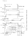
- the TFT charges point A to the low level Vs(l) of Vsig.
- the capacitive coupling potential ⁇ V* appears.
- the effective applied voltage Veff to the liquid crystal is, with respective to the picture signal amplitude Vsigpp, nearly Vsigpp + 2 ⁇ V* as shown in Fig.2(e), and the both superpose on each other.
- the output amplitude of the picture signal output IC can be decreased by 2 ⁇ V*.
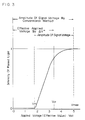
- FIG. 3 shows the relation of the applied voltage of liquid crystal and transmission light intensity, and also refers to an example of voltage range for controlling the transmitted light by ⁇ V* and Vsig.
- the voltage range in which the transmitted light of liquid crystal varies is from Vth to Vmax. Setting the applied voltage by ⁇ V* at VCT, by controlling the amplitude of the signal voltage and the phase, the required maximum signal amplitude voltage can decrease Vsigpp to (Vmax - Vth).
- FIG. 2 shows a case of matching of amplitude in the positive direction and negative direction of the first and second modulation signals.
- it is not possible to compensate the effect for inducing a DC potential difference between the mean potential of the picture element electrode and the mean potential of the picture signal wire through the coupling of the scanning signal voltage with parasitic capacitance.
- it possesses, as stated above, the effect of decreasing the picture signal amplitude, which is one of the objects of the invention.
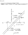
- FIG. 4 shows a driving method in which the waveform in FIG. 2 is further improved.
- amplitude Vt of the second modulation signal should be set at 3.4V in both positive direction and negative direction (see equation (5)).
- Their potential difference of 2.08V is applied, in FIG. 4, as the potential fluctuation of Ve in the ON period of TFT.
- the mean potential of the picture element electrode and the mean potential of the picture signal wire can be equalized. That is, the DC components of the both are zero, and are thus compensated.
- the phenomenon of image memory will be very slight as stated below.
- FIG. 6 shows a circuit diagram of the device of the first embodiment of the invention, in which numeral 11 is a scanning drive circuit, 12 is a video signal drive circuit, 13 is a first modulation circuit, and 14 is a second modulation circuit. Furthermore, 15a, 15b, ..., 15z are scanning signal wires, 16a, 16b, ..., 16z are image signal wires, 17a, 17b, ..., 17z are common electrodes of storage capacitance, and 18a, 18b, ..., 18z are counter electrodes of liquid crystal. In this embodiment, the storage capacitance and counter electrode are separated in each scanning signal wire as shown above, and the first and second modulation signals are applied according to each scanning signal wire. The time chart of scanning signal and modulation signal is shown in FIG. 7.
- This diagram shows the scanning signal and modulation signal corresponding to the N-th scanning signal wire and N+l-th scanning signal wire.
- the mutual relation of modulation signal and image signal, and ⁇ V* and Vsig is, intrinsically, same as shown in FIG. 2. That is, the polarity of image signal and modulation signal is inverted in every frame.
- Example 2 the displacement of the first modulation signals Ve(N), Ve(N+l) in the negative direction was varied in two steps as indicated by broken line in FIG. 7. That is, the Ve potential was once varied in ON period of TFT, and after the TFT was turned off, the modulation signal was added in the negative direction decreasing in the amplitude as compared with the displacement in the positive direction.
- the circuit of the third embodiment is shown in FIG. 8, and the voltage waveform applied to this circuit is given in FIG. 9.
- 21a is a first scanning signal wire
- 21a' is a common electrode wire of the storage capacitance attached to the first scanning signal wire
- 21z is a final scanning signal wire
- 21z' is a common electrode wire of storage capacitance attached to the first scanning signal wire.
- the common electrode of storage capacitance Cs was formed by using the scanning signal wire of the previous stage. Therefore, the first modulation signal is applied to the scanning signal wire of the preceding stage. As shown in FIG.
- the polarity inversion of the modulation signals may be effected either to the N-th and N+l-th scanning signal wires, or to the odd and even fields, or in duplication, or to the field alone.
- the potential variation of first modulation signal in the positive direction Ve(+) and the potential variation in the negative direction Ve(-) are designed to be variable independently.
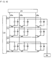
- the circuit of the fourth embodiment is shown in FIG. 10, and the voltage waveform applied in this example is given in FIG. 11.
- Example 3 it is same as in Example 3 that the first modulation signal is applied in duplication to the scanning signal wire, but the counter electrode is not divided into each corresponding scanning signal wire, and the potential is identical over the entire display device, and the electric polarity of the picture element electrode and counter electrode are varied in every scanning period (lH).
- 22 is a scanning drive circuit
- 24 is a video signal drive circuit
- 26 is a second modulation signal generation circuit.
- 25a, 25b, ..., 25z are picture signal wires.
- Ch(N), Ch(N+l) are voltage waveforms applied to the N-th and N+l-th scanning signal wires.
- Vt is a second modulation signal
- Vsig is a picture signal voltage waveform. This diagram also shows the difference in voltage waveform (polarity inversion) in the odd field and even field for AC driving of the liquid crystal.
- the higher waveform Vg of waveforms Ch(N), Ch(N+l) is a scanning signal, and the rectangular waveform linking to its front and rear is a first modulation signal Ve.
- the amplitude of Ve is controlled at identical voltage and fixed amplitude in all scanning signal wires. However, only the potentials Vge(+), Vge(-) indicated by thick lines right after scanning signal were controlled independently. Therefore, as the first modulation signal right after end of scanning signal, Vge(-)-Ve(+) is defined as the potential change in the positive direction, and Vge(+)-Ve(-) as the potential change in the negative direction.
- the application time Ts of the scanning signal is variable controllable within less than one scanning period. After termination of scanning of the next stage ⁇ Ch(N+l) ⁇ , following the delay time ⁇ d, first and second modulation signals were applied.
- Example 4 the potentials Vge(-), Vge(+) right after scanning signal were made equal to potential Ve(-), Ve(+), respectively.
- driving is not matched with the conditional formula (b) in one scanning period right after scanning signal, but in the other display periods, the driving conforms to the fundamental conditional formula (4b).
- the period conforming to (4b) is 238/240, which may practically be regarded as the whole period.
- Example 4 the potential of the second modulation signal generator 26 in FIG. 10 was made floating. That is, the counter electrode was not connected to any terminal, and the circuit was driven in the floating potential state.
- the first modulation signal Ve applied to all scanning signal wires appears at the counter electrode through the electrostatic capacitance in the display device.
- the display device Inside the display device, there is a picture signal wire held at a potential indifferent to Ve, and the second modulation signal appearing at the counter electrode is generally small in amplitude than Ve, and the condition formula (4b') is not satisfied perfectly.
- the source for generation of second modulation signal can be omitted, and the power saving effect is great. It is also possible to display excellent pictures, and the objects of the invention are satisfied almost completely.
- the second modulation signal generator 26 was composed of a capacitor. One of the electrodes of the capacitor was connected to the counter electrode, and the other electrode was connected to the first modulation signal generator.
- the capacitance of the capacitor it is enough when it is sufficiently larger than the capacitance between the counter electrodes of the display device and all picture signal wires, and it may not be so large as the capacitance between the counter electrodes and all electrodes on the other board.
- the second modulation signal generator is not particularly needed, and the power saving effect is great.
- Example 7 one of the electrodes of the resistance is connected parallel to the capacitor furthermore to the counter electrode connected to one of the electrodes of the capacitor, and the other electrode of the resistance was connected to an electrode held at a specific potential.
- the resistance value R of this resistance may be enough if the time constant CR is sufficiently larger than the period (l/H) of the modulation signal.
- Example 1 the common wires 17a, 17b, ..., 17z of storage capacitance were commonly connected, and furthermore the common wires 18a, 18b, ..., 18z of the counter electrode were commonly connected, and in this constitution the driving similar to Example 4 was effected by changing the polarity of display electrodes in every one scanning period. In this case, although it is impossible to render the internal DC potential difference to zero, a favourable picture display is realized.
- the output signal voltage of the signal drive circuit of the active matrix display device can be greatly decreased, and the power consumption of the same drive circuit handling analog signals is saved. Furthermore, when this invention is used in color display, the output amplitude of the chroma IC is also decreased, and the power of the circuit is also saved. Thus, the driving electric power of the entire display device can be decreased. On the other hand, decrease of the amplitude of the output signal voltage brings about secondary effects, such as ease of fabrication of circuit, use of region of good linearity of signal amplifier, and improvement of display quality, among the recent tendencies of higher display density and higher frequency of signal driving circuit.
- Example 4 in addition to the above, uniform brightness of display, and notable enhancement of gradation display performance were observed.
- the reliability of display device is enhanced. This is because of removal of the DC voltage conventionally occurring inevitably in the display device due to anisotropy of liquid crystal and capacitive coupling of scanning signal through Cgd. These DC voltage components were causes to induce various display defects. By removal of such DC voltage, the printing phenomenon of image occurring right after display of fixed image was greatly improved. Furthermore, the driving condition conforming to formula (4) is not affected by the dielectric anisotropy of the liquid crystal. It means that, when the display device is used in a wide temperature range, if the dielectric constant itself varies, its effects do not appear so that stable driving is guaranteed.
- this invention was applied in liquid crystal display device, but it may be also applied in driving of other flat plate display device.
Landscapes
- Engineering & Computer Science (AREA)
- Chemical & Material Sciences (AREA)
- Crystallography & Structural Chemistry (AREA)
- Physics & Mathematics (AREA)
- Computer Hardware Design (AREA)
- General Physics & Mathematics (AREA)
- Theoretical Computer Science (AREA)
- Power Engineering (AREA)
- Multimedia (AREA)
- Signal Processing (AREA)
- Liquid Crystal Display Device Control (AREA)
- Liquid Crystal (AREA)
Claims (11)
- Verfahren zum Ansteuern eines Anzeigegerätes, bei dem eine Wechselspannung an das Anzeigematerial angelegt wird und das Anzeigegerät umfaßt: Bildelement-Elektroden (7), die in in Matrixform angeordnet sind; Dünnfilmtransistoren (3), deren Drain-Elektroden, Source-Elektroden und Gate-Elektroden jeweils mit den Bildelement-Elektroden (7), mit Bildsignaldrähten (2) bzw. mit Abtastsignaldrähten (1) verbunden sind; erste Drähte (X), die mit den Bildelement-Elektroden (7) über Speicherkapazität (Cs) gekoppelt sind und Gegenelektroden (9), die den Bildelement-Elektroden (7) durch das Anzeigematerial (10) gegenüberliegend ausgebildet sind;
wobei:
das Anlegen der Wechselspannung ausgeführt wird durch Verändern des an dem Anzeigematerial (10) anliegenden Potentials unter Durchleiten von Bildsignal-Spannungen zu den Bildelement-Elektroden (7) während der EIN-Periode der entsprechenden TFTs (3), durch Anlegen von ersten Modulationssignalen (Ve) an die ersten Drähte (X) während der AUS-Periode der jeweiligen TFTs (3) und durch Anlegen von zweiten Modulationssignalen (Vt) an die Gegenelektroden (9) synchron zu den ersten Modulationssignalen (Ve). - Verfahren zum Ansteuern eines Anzeigegerätes nach Anspruch 1, bei dem dritte Modulationssignale synchron zu den ersten Modulationssignalen (Ve) an die Abtastsignaldrähte (1) angelegt werden.
- Verfahren zum Ansteuern eines Anzeigegerätes nach Anspruch 1 oder 2, bei dem die ersten Modulationssignale (Ve) und die zweiten Modulationssignale (Vt) die gleiche Polarität besitzen.
- Verfahren zum Ansteuern eines Anzeigegerätes nach Anspruch 1 oder 2, bei dem während einer Zeitperiode nach dem Ende der EIN-Periode der jeweiligen TFTs (3) erste Modulationssignale mit zwischen den positiven und negativen Richtungen unterschiedlichen Amplituden und von Feld zu Feld wechselnder Polarität an die ersten Drähte (X) angelegt werden.
- Verfahren zum Ansteuern eines Anzeigegerätes nach Anspruch 1, bei dem die ersten Drähte (X) einander benachbarte Abtastsignaldrähte sind.
- Verfahren zum Ansteuern eines Anzeigegerätes nach Anspruch 1 oder 2, bei dem vor dem Ende der EIN-Periode der jeweiligen TFTs (3) ein Teil des Potentials des ersten Modulationssignals (Ve) geändert wird.
- Verfahren zum Ansteuern eines Anzeigegerätes nach Anspruch 1 oder 2, bei dem die ersten Modulationssignale (Ve) und die zweiten Modulationssignale (Vt) die gleiche Amplitude besitzen.
- Verfahren zum Ansteuern eines Anzeigegerätes nach Anspruch 1, 2 oder 5, bei dem die Gegenelektroden (9) über die gesamte Anzeigefläche auf gleichmäßigem Potential gehalten werden, erste Modulationssignale (Ve), deren Polarität bei jeder Abtastperiode geändert wird, an die ersten Drähte (X) angelegt werden, und gleichzeitig die zweiten Modulationssignale (Vt) synchron mit den ersten Modulationssignalen (Ve) an die Gegenelektroden (9) angelegt werden.
- Verfahren zum Ansteuern eines Anzeigegerätes nach Anspruch 7, bei dem während einer Zeitperiode nach dem Anlegen der jeweiligen Abtastsignale die Amplituden der ersten Modulationssignale (Ve) in der positiven Richtung größer und in der negativen Richtung kleiner sind.
- Verfahren zum Ansteuern eines Anzeigegerätes nach Anspruch 1 oder 2, bei dem die Gegenelektroden (9) auf einem schwimmenden elektrischen Potential gehalten werden und die zweiten Modulationssignale (Vt) von den ersten Modulationssignalen (Ve) durch eine in dem Anzeigegerät bestehende kapazitive Kopplung zugeführt werden.
- Verfahren zum Ansteuern eines Anzeigegerätes nach Anspruch 10, bei dem die Gegenelektroden (9) auf einem bestimmten Potential gehalten werden und die zweiten Modulationssignale (Vt) durch eine kapazitive Kopplung von den ersten Modulationssignalen (Ve) zugeführt werden.
Applications Claiming Priority (2)
| Application Number | Priority Date | Filing Date | Title |
|---|---|---|---|
| JP5876588 | 1988-03-11 | ||
| JP58765/88 | 1988-03-11 |
Publications (2)
| Publication Number | Publication Date |
|---|---|
| EP0336570A1 EP0336570A1 (de) | 1989-10-11 |
| EP0336570B1 true EP0336570B1 (de) | 1994-01-12 |
Family
ID=13093639
Family Applications (1)
| Application Number | Title | Priority Date | Filing Date |
|---|---|---|---|
| EP89302407A Expired - Lifetime EP0336570B1 (de) | 1988-03-11 | 1989-03-10 | Ansteuerverfahren für eine Anzeigevorrichtung |
Country Status (3)
| Country | Link |
|---|---|
| US (1) | US5706023A (de) |
| EP (1) | EP0336570B1 (de) |
| DE (1) | DE68912173T2 (de) |
Families Citing this family (34)
| Publication number | Priority date | Publication date | Assignee | Title |
|---|---|---|---|---|
| JPH03168617A (ja) * | 1989-11-28 | 1991-07-22 | Matsushita Electric Ind Co Ltd | 表示装置の駆動方法 |
| EP0456453B1 (de) * | 1990-05-07 | 1995-09-06 | Fujitsu Limited | Anzeigeeinrichtung von höher Qualität mit aktiver Matrix |
| TW207570B (en) * | 1991-10-04 | 1993-06-11 | Toshiba Co Ltd | Method for automatically detecting drill blade of the drill bit specified for drilling hole on PC board |
| JP3069930B2 (ja) * | 1992-02-28 | 2000-07-24 | キヤノン株式会社 | 液晶表示装置 |
| JPH0667145A (ja) * | 1992-08-24 | 1994-03-11 | Hitachi Ltd | 液晶表示装置 |
| KR940009734A (ko) | 1992-10-29 | 1994-05-24 | 카나이 쯔또무 | 매트릭스형 표시장치 및 그 구동방법 |
| JPH06289817A (ja) * | 1993-04-01 | 1994-10-18 | Sharp Corp | 表示装置の駆動方法及び駆動回路 |
| EP0622655A3 (de) * | 1993-04-22 | 1995-09-13 | Matsushita Electric Industrial Co Ltd | Anzeigevorrichtung, Verfahren zu ihrer Steuerung, und Anzeigeeinrichtung vom Projectionstyp mit derselben. |
| US5986631A (en) * | 1995-07-05 | 1999-11-16 | Matsushita Electric Industrial Co., Ltd. | Method for driving active matrix LCD using only three voltage levels |
| JP3069280B2 (ja) * | 1995-12-12 | 2000-07-24 | 松下電器産業株式会社 | アクティブマトリックス型液晶表示素子及びその駆動方法 |
| US5949398A (en) * | 1996-04-12 | 1999-09-07 | Thomson Multimedia S.A. | Select line driver for a display matrix with toggling backplane |
| GB2333634B (en) * | 1998-01-21 | 2002-02-20 | Sharp Kk | Liquid crystal device and method of addressing liquid crystal device |
| JP3006586B2 (ja) | 1998-06-01 | 2000-02-07 | 日本電気株式会社 | アクティブマトリクス型液晶表示装置 |
| US6985142B1 (en) * | 1998-09-03 | 2006-01-10 | University Of Southern California | Power-efficient, pulsed driving of capacitive loads to controllable voltage levels |
| KR100590746B1 (ko) * | 1998-11-06 | 2006-10-04 | 삼성전자주식회사 | 서로다른공통전압을가지는액정표시장치 |
| US6909415B2 (en) * | 2000-04-24 | 2005-06-21 | Matsushita Electric Industrial Co., Ltd. | Display unit and drive method therefor |
| JP3723747B2 (ja) * | 2000-06-16 | 2005-12-07 | 松下電器産業株式会社 | 表示装置およびその駆動方法 |
| JP4330059B2 (ja) * | 2000-11-10 | 2009-09-09 | カシオ計算機株式会社 | 液晶表示装置及びその駆動制御方法 |
| JP3832240B2 (ja) * | 2000-12-22 | 2006-10-11 | セイコーエプソン株式会社 | 液晶表示装置の駆動方法 |
| EP1239444A1 (de) * | 2001-03-06 | 2002-09-11 | Matsushita Electric Industrial Co., Ltd. | Flüssigkristallanzeigevorrichtung und Ansteuerungsverfahren dafür |
| JP2002278517A (ja) * | 2001-03-15 | 2002-09-27 | Hitachi Ltd | 液晶表示装置 |
| GB0216904D0 (en) * | 2002-07-20 | 2002-08-28 | Koninkl Philips Electronics Nv | Active matrix liquid crystal display device |
| US20040068293A1 (en) * | 2002-10-04 | 2004-04-08 | Howard Scalzo | Packaged antimicrobial medical device and method of preparing same |
| JP2004191581A (ja) * | 2002-12-10 | 2004-07-08 | Sharp Corp | 液晶表示装置およびその駆動方法 |
| TW588320B (en) * | 2003-03-07 | 2004-05-21 | Hannstar Display Corp | Liquid crystal display |
| US20040222953A1 (en) * | 2003-05-06 | 2004-11-11 | Smith Joseph T. | Low voltage frame buffer for high contrast LCD microdisplay and method therefor |
| CN101533609B (zh) * | 2003-08-19 | 2012-07-04 | 伊英克公司 | 电光显示器及操作电光显示器的方法 |
| EP2698784B1 (de) * | 2003-08-19 | 2017-11-01 | E Ink Corporation | Elektrooptischer Bildschirm |
| US8164562B2 (en) * | 2006-10-24 | 2012-04-24 | Samsung Electronics Co., Ltd. | Display device and driving method thereof |
| JP4873760B2 (ja) * | 2007-03-16 | 2012-02-08 | シャープ株式会社 | 液晶表示装置およびその駆動方法 |
| US7928941B2 (en) * | 2007-03-20 | 2011-04-19 | Sony Corporation | Electro-optical device, driving circuit and electronic apparatus |
| JPWO2009113223A1 (ja) * | 2008-03-11 | 2011-07-21 | シャープ株式会社 | 駆動回路、駆動方法、液晶表示パネル、液晶モジュール、および液晶表示装置 |
| GB2481008A (en) | 2010-06-07 | 2011-12-14 | Sharp Kk | Active storage pixel memory |
| US9310916B2 (en) | 2011-01-14 | 2016-04-12 | Apple Inc. | Display to touch crosstalk compensation |
Family Cites Families (15)
| Publication number | Priority date | Publication date | Assignee | Title |
|---|---|---|---|---|
| GB2064194B (en) * | 1978-02-08 | 1982-08-04 | Sharp Kk | Matrix type liquid crystal display device |
| GB2050668B (en) * | 1979-05-28 | 1983-03-16 | Suwa Seikosha Kk | Matrix liquid crystal display system |
| FR2524679B1 (fr) * | 1982-04-01 | 1990-07-06 | Suwa Seikosha Kk | Procede d'attaque d'un panneau d'affichage a cristaux liquides a matrice active |
| JPS59116685A (ja) * | 1982-12-23 | 1984-07-05 | セイコーインスツルメンツ株式会社 | 画像表示装置 |
| JPS59119390A (ja) * | 1982-12-25 | 1984-07-10 | 株式会社東芝 | 薄膜トランジスタ回路 |
| JPS59157693A (ja) * | 1983-02-28 | 1984-09-07 | シチズン時計株式会社 | 表示装置の駆動方法 |
| JPS603698A (ja) * | 1983-06-21 | 1985-01-10 | ソニー株式会社 | 液晶デイスプレイ装置 |
| JPS6066236A (ja) * | 1983-09-21 | 1985-04-16 | Canon Inc | 液晶デイスプレイパネルの駆動法 |
| JPS60151615A (ja) * | 1984-01-19 | 1985-08-09 | Matsushita Electric Ind Co Ltd | 液晶表示デバイス駆動法 |
| JPS60156095A (ja) * | 1984-11-22 | 1985-08-16 | ソニー株式会社 | 液晶デイスプレイ装置 |
| JP2583211B2 (ja) * | 1985-05-10 | 1997-02-19 | シチズン時計株式会社 | 液晶表示装置 |
| JPS61275822A (ja) * | 1985-05-31 | 1986-12-05 | Seiko Epson Corp | 液晶表示装置の駆動方法 |
| JPS61275823A (ja) * | 1985-05-31 | 1986-12-05 | Seiko Epson Corp | 液晶表示装置 |
| JPS61275824A (ja) * | 1985-05-31 | 1986-12-05 | Seiko Epson Corp | 液晶表示装置 |
| KR920007167B1 (ko) * | 1987-04-20 | 1992-08-27 | 가부시기가이샤 히다씨세이사구쇼 | 액정표시장치 및 그 구동방법 |
-
1989
- 1989-03-10 EP EP89302407A patent/EP0336570B1/de not_active Expired - Lifetime
- 1989-03-10 DE DE68912173T patent/DE68912173T2/de not_active Expired - Lifetime
-
1995
- 1995-06-07 US US08/487,704 patent/US5706023A/en not_active Expired - Lifetime
Also Published As
| Publication number | Publication date |
|---|---|
| US5706023A (en) | 1998-01-06 |
| DE68912173D1 (de) | 1994-02-24 |
| EP0336570A1 (de) | 1989-10-11 |
| DE68912173T2 (de) | 1994-05-19 |
Similar Documents
| Publication | Publication Date | Title |
|---|---|---|
| US5706023A (en) | Method of driving an image display device by driving display materials with alternating current | |
| KR920009030B1 (ko) | 표시장치의 구동방법 | |
| US5398043A (en) | Driving method for a display device | |
| US5151805A (en) | Capacitively coupled driving method for TFT-LCD to compensate for switching distortion and to reduce driving power | |
| US5995074A (en) | Driving method of liquid crystal display device | |
| US6040814A (en) | Active-matrix liquid crystal display and method of driving same | |
| KR0144450B1 (ko) | 액정표시장치 | |
| KR0127105B1 (ko) | 표시장치의 구동 방법 및 회로 | |
| EP0657864B1 (de) | Verfahren zum wechselstromtreiben einer flüssigkeitskristallanzeige und anzeige dafür | |
| EP0436384B1 (de) | Treiberschaltung für ein Flüssigkristallanzeigegerät | |
| JP2737209B2 (ja) | 表示装置の駆動方法 | |
| JP2730286B2 (ja) | 表示装置の駆動方法 | |
| KR100483400B1 (ko) | 액정표시장치의구동방법 | |
| KR100229621B1 (ko) | 액티브 매트릭스형 액정표시장치의 구동방법 | |
| JP3140088B2 (ja) | 液晶表示装置の駆動方法 | |
| KR0147119B1 (ko) | 누설전류 보상을 위한 액정구동장치 | |
| JP3437866B2 (ja) | 表示装置の駆動方法 | |
| JP2809950B2 (ja) | 表示装置の駆動方法 | |
| JP3431260B2 (ja) | 表示装置の駆動方法 | |
| JPH09179098A (ja) | 表示装置 | |
| KR20080054549A (ko) | 액정 표시 장치 | |
| KR100205427B1 (ko) | 액정표시장치의 데이터샘플링 홀더회로 및 그 구동방법 | |
| JPH0343786A (ja) | アクティブマトリックス液晶パネル用信号処理回路 | |
| JPH08334741A (ja) | 液晶装置 | |
| JPH05204337A (ja) | 画素書き込み電圧補償駆動方式 |
Legal Events
| Date | Code | Title | Description |
|---|---|---|---|
| PUAI | Public reference made under article 153(3) epc to a published international application that has entered the european phase |
Free format text: ORIGINAL CODE: 0009012 |
|
| AK | Designated contracting states |
Kind code of ref document: A1 Designated state(s): DE FR GB |
|
| 17P | Request for examination filed |
Effective date: 19891205 |
|
| 17Q | First examination report despatched |
Effective date: 19920326 |
|
| GRAA | (expected) grant |
Free format text: ORIGINAL CODE: 0009210 |
|
| AK | Designated contracting states |
Kind code of ref document: B1 Designated state(s): DE FR GB |
|
| REF | Corresponds to: |
Ref document number: 68912173 Country of ref document: DE Date of ref document: 19940224 |
|
| ET | Fr: translation filed | ||
| PLBE | No opposition filed within time limit |
Free format text: ORIGINAL CODE: 0009261 |
|
| STAA | Information on the status of an ep patent application or granted ep patent |
Free format text: STATUS: NO OPPOSITION FILED WITHIN TIME LIMIT |
|
| 26N | No opposition filed | ||
| REG | Reference to a national code |
Ref country code: GB Ref legal event code: 746 Effective date: 19951123 |
|
| REG | Reference to a national code |
Ref country code: FR Ref legal event code: D6 |
|
| REG | Reference to a national code |
Ref country code: GB Ref legal event code: IF02 |
|
| REG | Reference to a national code |
Ref country code: GB Ref legal event code: 732E |
|
| REG | Reference to a national code |
Ref country code: FR Ref legal event code: TP |
|
| PGFP | Annual fee paid to national office [announced via postgrant information from national office to epo] |
Ref country code: GB Payment date: 20080305 Year of fee payment: 20 |
|
| PGFP | Annual fee paid to national office [announced via postgrant information from national office to epo] |
Ref country code: FR Payment date: 20080311 Year of fee payment: 20 Ref country code: DE Payment date: 20080306 Year of fee payment: 20 |
|
| REG | Reference to a national code |
Ref country code: GB Ref legal event code: PE20 Expiry date: 20090309 |
|
| PG25 | Lapsed in a contracting state [announced via postgrant information from national office to epo] |
Ref country code: GB Free format text: LAPSE BECAUSE OF EXPIRATION OF PROTECTION Effective date: 20090309 |