EP0335748B1 - Schaltung zum Identifizieren der Aufzeichnungsbetriebsart und ein diese Schaltung enthaltendes Wiedergabegerät - Google Patents
Schaltung zum Identifizieren der Aufzeichnungsbetriebsart und ein diese Schaltung enthaltendes Wiedergabegerät Download PDFInfo
- Publication number
- EP0335748B1 EP0335748B1 EP89303233A EP89303233A EP0335748B1 EP 0335748 B1 EP0335748 B1 EP 0335748B1 EP 89303233 A EP89303233 A EP 89303233A EP 89303233 A EP89303233 A EP 89303233A EP 0335748 B1 EP0335748 B1 EP 0335748B1
- Authority
- EP
- European Patent Office
- Prior art keywords
- signal
- mode
- reproduced
- level
- component
- Prior art date
- Legal status (The legal status is an assumption and is not a legal conclusion. Google has not performed a legal analysis and makes no representation as to the accuracy of the status listed.)
- Expired - Lifetime
Links
Images


Classifications
-
- H—ELECTRICITY
- H04—ELECTRIC COMMUNICATION TECHNIQUE
- H04N—PICTORIAL COMMUNICATION, e.g. TELEVISION
- H04N9/00—Details of colour television systems
- H04N9/79—Processing of colour television signals in connection with recording
- H04N9/80—Transformation of the television signal for recording, e.g. modulation, frequency changing; Inverse transformation for playback
- H04N9/82—Transformation of the television signal for recording, e.g. modulation, frequency changing; Inverse transformation for playback the individual colour picture signal components being recorded simultaneously only
- H04N9/83—Transformation of the television signal for recording, e.g. modulation, frequency changing; Inverse transformation for playback the individual colour picture signal components being recorded simultaneously only the recorded chrominance signal occupying a frequency band under the frequency band of the recorded brightness signal
-
- H—ELECTRICITY
- H04—ELECTRIC COMMUNICATION TECHNIQUE
- H04N—PICTORIAL COMMUNICATION, e.g. TELEVISION
- H04N9/00—Details of colour television systems
- H04N9/79—Processing of colour television signals in connection with recording
- H04N9/87—Regeneration of colour television signals
-
- H—ELECTRICITY
- H04—ELECTRIC COMMUNICATION TECHNIQUE
- H04N—PICTORIAL COMMUNICATION, e.g. TELEVISION
- H04N9/00—Details of colour television systems
- H04N9/79—Processing of colour television signals in connection with recording
- H04N9/80—Transformation of the television signal for recording, e.g. modulation, frequency changing; Inverse transformation for playback
- H04N9/82—Transformation of the television signal for recording, e.g. modulation, frequency changing; Inverse transformation for playback the individual colour picture signal components being recorded simultaneously only
- H04N9/83—Transformation of the television signal for recording, e.g. modulation, frequency changing; Inverse transformation for playback the individual colour picture signal components being recorded simultaneously only the recorded chrominance signal occupying a frequency band under the frequency band of the recorded brightness signal
- H04N9/832—Transformation of the television signal for recording, e.g. modulation, frequency changing; Inverse transformation for playback the individual colour picture signal components being recorded simultaneously only the recorded chrominance signal occupying a frequency band under the frequency band of the recorded brightness signal using an increased bandwidth for the luminance or the chrominance signal
- H04N9/833—Transformation of the television signal for recording, e.g. modulation, frequency changing; Inverse transformation for playback the individual colour picture signal components being recorded simultaneously only the recorded chrominance signal occupying a frequency band under the frequency band of the recorded brightness signal using an increased bandwidth for the luminance or the chrominance signal with selection of the conventional or the increased bandwidth signal, e.g. VHS or SVHS signal selection
-
- H—ELECTRICITY
- H04—ELECTRIC COMMUNICATION TECHNIQUE
- H04N—PICTORIAL COMMUNICATION, e.g. TELEVISION
- H04N9/00—Details of colour television systems
- H04N9/79—Processing of colour television signals in connection with recording
- H04N9/87—Regeneration of colour television signals
- H04N9/898—Regeneration of colour television signals using frequency multiplication of the reproduced colour signal carrier with another auxiliary reproduced signal, e.g. a pilot signal carrier
Definitions
- This invention relates to detecting the mode of a reproduced colour video signal, and more particularly to recording mode identifying circuits suitable for use in a magnetic recording and/or reproducing apparatus capable of selective operation in a low-band mode and a high-band mode, and to apparatus for reproducing a colour video signal.
- VTR rotary video tape recorder
- FM frequency modulated
- chroma signal is down-converted to a low frequency region for recording in oblique tracks on a magnetic tape
- horizontal resolution can be improved, and consequently high picture quality can be achieved, by increasing the carrier frequency that is frequency modulated by the luminance signal. Therefore, it has been recommended that a VTR be provided with a mode in which recording is carried out with the carrier freqeuncy used for frequency modulating the luminance signal higher than the carrier frequency usually used in such a VTR.
- the carrier frequency for the frequency modulation by the luminance signal is usually set to be 4.2 MHz at the sync tip level and 5.4 MHz at the white peak level, and it has been suggested that recording be performed with a higher carrier frequency, that is, with a carrier frequency which is 5.7 MHz at the sync tip level and 7.7 MHz at the white peak level.
- a mode in which the carrier freqeuncy for the frequency modulation by the luminance signal is increased hereinafter called the "high-band mode”
- the low-band mode a mode in which the carrier freqeuncy for the frequency modulation by the luminance signal is increased
- a VTR equipped with a mode identifying circuit for automatically determining whether the video signal was recorded on the reproduced tape in the low-band mode or the high-band mode.
- a mode identifying circuit detects a signal level of a predetermined frequency component which is comprised in a recorded signal of one mode, and determines whether this detection level is equal to, or above a predetermined level, as the basis for a mode identification.
- FIG. 1 An example of such a mode identification circuit is shown in Figure 1 in which a reproduced FM luminance signal Y FM is supplied from an input terminal 100 to a band-pass filter 101 which passes a frequency component of a frequency f L which is included in the FM luminance signal Y FM and corresponds, for example, to the sync tip level of the video signal when recorded in the low-band mode.
- a band-pass filter 101 which passes a frequency component of a frequency f L which is included in the FM luminance signal Y FM and corresponds, for example, to the sync tip level of the video signal when recorded in the low-band mode.
- the output of the band-pass filter 101 is supplied to a detector 102 which detects the level of the frequency component corresponding to the carrier frequency f L .
- the output of the detector 102 is applied to a negative input of a comparator 103 which receives a reference voltage at a positive input thereof.
- the comparator 103 detects whether the output level of the detector 102 is equal to or greater than the predetermined reference voltage, and the resulting output of the comparator 103 is available at an output terminal 104 as a mode identifying output.
- the output level of the detector 102 becomes equal to or greater than the reference voltage.
- the output of the comparator 103 assumes a negative or low level.
- the reproduced FM luminance signal, Y FM is a high-band signal, it is intended that no signal equal to or larger than the reference voltage is detected at the detector 102, and that, as a result thereof, the output of the comparator 103 will assume a high level for identifying the high-band signal.
- Figure 2 shows another example of a proposed mode identifying circuit in which the reproduced FM luminance signal is supplied from an input terminal 110 to a band-pass filter 111 which, for example, passes the frequency component f L corresponding to the sync tip level in the case of the low-band mode, and also to a band-pass filter 112 which, for example, passes a frequency component F H corresponding to the sync tip level in the case of the high-band mode.
- the output of the band-pass filter 111 is supplied to a detector 113, and the output of the detector 113 is applied to a negative input of a comparator 115.
- the output of the band-pass filter 112 is supplied to a detector 114, and the output of the detector 114 is reapplied to a positive input of the comparator 115.
- the resulting output of the comparator 115 is made available at an output terminal 116 as a mode identifying signal.
- the output level of the detector 113 is larger than the output level of the detector 114, so that the output of the comparator 115 is a negative or low level signal for identifying the low-band signal.
- the output of the detector 114 is larger than the output of the detector 113 and, therefore, the output of the comparator 115 is at a high level to identify the high-band signal.
- a frequency component of the lower sideband is passed by the band-pass filter 101, and a signal equal to or greater than the predetermined level may be detected at the detector 102. Therefore, the output of the comparator 103 may assume a low level despite the fact that the reproduced FM luminance signal Y FM was recorded in the high-band mode, and it is erroneously indicated that the video signal being reproduced was recorded in the low-band mode.
- the carrier of the FM luminance signal during each synchronization signal interval has a predetermined frequency and its sideband components are spread in a predetermined manner.
- the predetermined frequency component in the reproduced FM luminance signal Y FM only during each synchronization interval for identifying the recording mode, only a carrier component of the low-band mode can be detected, and an erroneous mode identification due to the influence of the lower sideband component of a reproduced FM luminance signal recorded in the high-band mode can be prevented.
- a recording mode identifying circuit for determining whether a reproduced FM signal was recorded in a first mode in which recording is effected with frequency modulation of a first carrier frequency by an information signal or in a second mode in which recording is effected with frequency modulation of a second carrier frequency by the information signal
- said mode identifying circuit being characterized by: phase inverting means for inverting a predetermined frequency component of a reproduced FM signal which corresponds to the frequency of the carrier of one of said first and second modes when modulated by a predetermined information signal level; limiter means for eliminating an amplitude modulation component of an output of said phase inverting means; and level detecting means for detecting a level of said predetermined frequency component in the reproduced FM signal which has had said predetermined frequency component inverted and said amplitude modulation component eliminated, whereby the mode with which said reproduced FM signal was recorded is determined from said level detected by said level detecting means.
- an apparatus for reproducing a colour video signal composed of a luminance signal and a chroma signal, and which is recorded on a magnetic tape according to a first mode in which recording is effected with frequency modulation of a first carrier frequency by said luminance signal or according to a second mode in which recording is effected with frequency modulation of a second carrier frequency by said luminance signal said apparatus comprising: magnetic head means for reproducing said colour video signal recorded on the magnetic tape; separation circuit means for separating the reproduced colour video signal from said magnetic head means into an FM luminance signal and a chroma signal; processing circuit means for processing the separated chroma signal; FM demodulation means which is selectively operative in one of first and second demodulation modes for demodulating the separated FM luminance signal when the colour video signal is recorded in a corresponding one of said first and second modes, respectively; and de-emphasis means for de-emphasizing the demodulated luminance signal from said FM demodulating means; characterized
- the phase inverter includes band-pass filter means receiving said reproduced FM luminance signal and arranged to pass said predetermined frequency component thereof, amplifying means receiving said predetermined frequency component passed by said band-pass filter means and operative to effect amplification by two thereof, and subtracting means for subtracting the two-fold or doubly amplified predetermined frequency component from said reproduced FM luminance signal and, as a result thereof, providing the reproduced FM luminance signal with the phase of said predetermined frequency component inverted therein.
- the recording mode is identified from the level of a frequency component of the reproduced FM luminance signal corresponding to the carrier frequency f1 for a sync tip level recorded in a low-band mode; the phase of the component of the frequency f1 of the reproduced FM luminance signal is inverted and its amplitude modulation component is eliminated.
- the lower sideband of the high-band mode includes the frequency f1
- the lower sideband of the high-band mode at the frequency f1 is suppressed.
- the level of the frequency component f1 of the reproduced FM luminance signal whose lower sideband in the high-band mode is suppressed at the frequency f1 is detected for identifying the recording mode. Since the lower sideband in the high-band mode at the frequency f1 is suppressed, an erroneous identification of the mode due to the influence of sideband components can be prevented.
- the invention can advantageously be applied to a VTR in which a video signal recorded with a high-band, or a video signal recorded with a low-band can be selectively reproduced.
- Figure 4A is a spectrum of a signal recorded in a low-band mode in an 8-mm VTR
- Figure 4B is a spectrum of a signal recorded in a high-band mode in an 8-mm VTR.
- Y FM is an FM luminance signal
- C is a so-called down-converted chroma signal
- a FM is an FM audio signal
- P is the spectrum of pilot signals for ATF tracking.
- the carrier frequency of the FM luminance signal Y FM is selected so that, as shown in Figure 4A, a frequency of 4.2 MHz corresponds to the sync tip level and a frequency of 5.4 MHz corresponds to the white peak level.
- the carrier frequency is selected so that the sync tip level is at a frequency of 5.7 MHz and the white peak level is at a frequency of 7.7 MHz.
- the centre frequency of the down-converted chroma signal is selected to be 743 kHz, and a centre frequency of the FM audio signal A FM is selected to be 1.5 MHz.
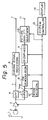
- a signal recorded on a magnetic tape 1 is reproduced by a rotated head 2, and the reproduced signal is supplied to a regenerative amplifier 3 through a rotary transformer (not shown).
- the output of the amplifier 3 is supplied to a band-pass filter 4 and a high-pass filter 5.
- a reproduced down-converted chroma signal C is obtained from the output of the band-pass filter 4, and a reproduced FM luminance signal Y FM is obtained from the output of the high-pass filter 5.
- the reproduced down-converted chroma signal C is supplied to a chroma signal processing circuit 6 in which, for example, time-axis variations of the reproduced signal and cross-talk components are eliminated. Moreover, in the processing circuit 6, the reproduced down-converted chroma signal C is returned to a chroma signal having a standard sub-carrier frequency, for example, of 3.58 MHz. A processed chroma signal is supplied from the output of the processing circuit 6 to an output terminal 7.
- a reproduced FM luminance signal Y FM obtained from the band-pass filter 5 is supplied to an FM demodulator 8 where a luminance signal is derived.
- the output of the demodulator 8 is supplied through a de-emphasis circuit 9 and a picture-quality adjusting circuit 10 to a respective output terminal 11.
- the VTR of Figure 5 it is possible to establish whether recording was effected in a high-band mode in which the picture quality is improved through the use of an increased carrier frequency at the time of frequency modulation of a luminance signal, or if recording was effected in the usual low-band mode.
- the FM luminance signal Y FM separated by the high-pass filter 5 is supplied to a mode identifying circuit 12 which determines whether the signal being reproduced from the tape 1 was recorded in the high-band mode or the low-band mode.
- the output of the mode identifying circuit 12, which identifies the recording mode, is supplied to the regenerative amplifier 3, the FM demodulator 8, the de-emphasis circuit 9, and the picture-quality-adjusting circuit 10, respectively, for controlling or changing-over the regenerative amplifier 3, the FM demodulator 8, the de-emphasis circuit 9, and the picture-quality-adjusting circuit 10 so that the characteristics thereof will at all times be suitable to accommodate the reproduced signal whether the latter was recorded in the low-band mode or the high-band mode as indicated by the output from the mode identifying circuit 12.
- the output of the mode identifying circuit 12 is also supplied to a system controller 13, for example, in the form of a microprocessor.
- An output of the system controller 13 is applied to a display unit 14, so that the mode in which the signal was recorded on the tape 1 being played-back or reproduced is displayed on the display unit 14.
- a user can readily ascertain which recording mode was employed for the recording in on the tape 1.
- the mode identifying circuit 12 relies for its operation on the fact that the carrier frequencies are different for recording in the low-band mode and for recording in the high-band mode.
- the mode identifying circuit 12 the level of a frequency component of the reproduced FM luminance signal having a frequency f1 corresponding to the sync tip level at the time of low-band recording is detected and the mode identification is effected on the basis of whether the frequency component of the frequency f1 is equal to or larger than a predetermined level.
- the mode identification is effected on the basis of whether the frequency component of the frequency f1 is equal to or larger than a predetermined level.
- the lower sideband component of the frequency f1 present in the reproduced FM luminance signal which was recorded in the high-band mode is substantially eliminated, whereupon the level of the component of the frequency f1 can be detected without the possibility of error.
- the lower sideband component of the frequency f1 in a reproduced FM luminance signal which was recorded in the high-band mode is suppressed by inverting the phase of the component of the frequency f1 and eliminating a resulting amplitude component by a limiter.
- ⁇ o is the angular velocity of the carrier
- J n (m f ) denotes a Bessel function
- m f is the modulation index
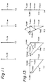
- an FM signal can be represented by a spectrum diagram as shown in Figure 6, and in which the sidebands spread upward and downward from the carrier CAR as a centre.
- the first-order sidebands LSB1 and USB1, and the third-order sidebands LSB3 and USB3, which are sidebands of an odd-number order are made so that their upper sidebands and lower sidebands are inverted in respect to one another.
- the second-order sideband components LSB2 and USB2, and the fourth-order sideband components LSB4 and USB4, which are sidebands of an even-number order, are made so that their upper sidebands and lower sidebands have the same phase as each other.
- the FM signal may be represented by the vector diagram of Figure 7 which shows an FM signal vector F FM over its second-order sideband component.
- a carrier vector V car is rotated with the angular velocity ⁇ o ;
- a first-order upper sideband vector V USB1 is rotated with the angular velocity p;
- a first-order lower sideband vector V LSB1 is rotated with an angular velocity -p;
- a second-order upper sideband vector V USB2 is rotated with an angular velocity 2p;
- a second-order lower sideband vector V LSB2 is rotated with an angular velocity -2p.
- the first-order lower sideband LSB1 of the high-band mode coincides with the frequency f1 for the purposes of this explanation of how the first-order sideband LSB1 with the frequency f1 can be suppressed by eliminating an amplitude component after inverting the component of the frequency f1. Similar explanations can be provided for the cases where the lower sidebands LSB1, LSB3 and LSB5, respectively, of an odd-number order coincide with the frequency f1.
- the first-order upper sideband USB1 has the same phase as the first-order lower sideband LSB1 as shown in Figure 8B.
- an AM component is derived from the first-order sideband component.
- Such an AM component can be eliminated by amplitude limitation by a limiter. More specifically, when a signal with the spectrum shown in Figure 8B is applied to the limiter, and the AM component shown in Figure 8C is added equivalently, the upper sideband USB1 and the lower sideband LSB1 are suppressed, as shown in Figure 8D.
- the carrier vector V CAR is rotated with the angular velocity ⁇ o
- the first-order upper sideband vector V USB1 is rotated with the angular velocity p
- the first-order lower sideband V LSB1 is rotated with the angular velocity -p.
- the vector diagram of the FM signal over the first-order sideband at each of times t1 to t4 is as shown in Figure 9. It is to be noted that for facilitating understanding, only the first-order upper sideband vector V USB1 and the first order lower sideband V LSB1 are shown to be rotated and the carrier vector V CAR is shown in a fixed position in the drawing, that is, not rotated.
- the length of the FM signal vector V FM hardly varies at the times t1 to t4 when the first-order sideband vectors V LSB1 and V USB1 are small. In other words, the amplitude of the FM signal barely changes.
- the vector V FM1 of a signal at each of the times t1 to t4 has an amplitude component that is substantially influenced by the first-order sideband, as indicated in Figure 10.
- the length of the signal vector V FM1 is different at each of the times t1 to t4.
- the first-order upper sideband USB1 and the inverted first-order lower sideband LSB1 are eliminated so as to provide only a vector V LIM corresponding to a carrier vector CAR.
- the second-order sideband LSB2 present in the frequency f1 can be suppressed by eliminating an amplitude modulation (AM) component after inversion of the component of the frequency f1 when the second-order lower sideband LSB2 of the signal recorded with high-band mode coincides with the frequency f1. Similar explanations can be provided for the cases where the lower sidebands of an even-number order LSB2, LSB4 .... coincides with the frequency f1.
- AM amplitude modulation
- the FM signal over its second-order sideband may be represented by the vector diagram of Figure 13, in which the carrier vector V CAR is shown not rotated for facilitating understanding, thereof. As is apparent from Figure 13, the amplitude of the FM signal vector V FM hardly varies at the times t11 to t14.
- the signal vector V FM1 becomes as shown in Figure 14. More specifically, when the second-order lower sideband vector V LSB2 of the FM signal shown in Figure 13 is inverted, the vector V FM of a signal at the times t11 to t14 has an amplitude modulation (AM) component since the lengths of the signal vector V FM1 at the times t11 to t14, respectively, are different from each other.
- AM amplitude modulation
- the signal represented in Figure 14 is supplied to the limiter for the elimination of its amplitude modulation (AM) component.
- AM amplitude modulation
- an amplitude component is added so that a signal vector V LIM at each of the times t11 to t14 becomes almost constant.
- the second-order lower sideband vector V LSB2 is cancelled and the second order upper sideband V USB2 is increased two-fold.
- the mode identifying circuit 12 suppresses a sideband component having the frequency f1 by inverting a signal component of the frequency corresponding to the sync tip level of the low-band mode, for example, and eliminating an amplitude modulation (AM) component by means of a limiter, and then detects the signal level of the frequency f1 as the basis for identifying the recording mode.
- AM amplitude modulation
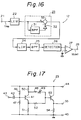
- a reproduced FM luminance signal Y FM is supplied from an input terminal 21 through a limiter 22 to a phase inverting circuit 23.
- the phase inverting circuit 23 inverts only the phase of a predetermined frequency f1, for example, the phase of a component having the frequency corresponding to the sync tip level in the low-band recording mode.
- the pedestal level may be used instead of the sync tip level.
- the output of the phase inverting circuit 23 is supplied to a limiter 24 in which amplitude modulation (AM) components of the output of the phase inverting circuit 23 are eliminated.
- the output of the limiter 24 is supplied to a band-pass filter 25.
- a circuit for suppressing such sideband is constituted by the phase inverting circuit 23 and the limiter 24.
- the lower sideband of a reproduced video signal which was recorded in the high-band mode includes the frequency f1 such lower sideband is suppressed by the phase inverting circuit 23 and the limiter 24.
- the band-pass filter 25 permits passage of a component of a predetermined frequency, for example, the frequency f1 corresponding to the sync tip level when recording with low-band mode.
- the output of the band-pass filter 25 is supplied to a detector 26 which detects the level of the component of the frequency f1 of the reproduced FM luminance signal Y FM through the limiter 22, the phase inverting circuit 23 and the limiter 24.
- the output of the detector 26 is applied to a negative input of a comparator 27.
- the comparator 27 detects whether the component level of the frequency f1 of the reproduced FM luminance signal Y FM obtained through the limiter 22, the phase inverting circuit 23, the limiter 24 and the band-pass filter 25 is equal to or above a predetermined reference level established by a reference voltage applied to a positive input of the comparator 27.
- the output of the comparator 27 is applied to an output terminal 28 as a mode identifying signal M det .
- the circuit for suppressing the sideband of the frequency f1 is composed of the phase inverting circuit 23 and the limiter 24. More particularly, the component of the frequency f1 is suppressed by the phase inverting circuit 23 and the limiter 24 when the component of the frequency f1 of the reproduced FM luminance signal is the lower sideband of the signal recorded in the high-band mode. As a result, only a carrier component of the frequency f1 of the reproduced FM luminance signal Y FM which corresponds to the low-band sync tip is detected at the detector 26.
- the carrier component of the frequency f1 corresponding to the sync tip level of the low-band mode is produced and passes through the band-pass filter 25 so that the output level of the detector 26 is equal to or above the level of the reference voltage applied to the positive input of the comparator 27.
- the mode identifying signal M det is at a low negative level when the reproduced video signal was recorded in the low-band mode.
- the output level of the detector 26 becomes substantially less than the predetermined value even if the lower sideband component of the frequency f1 lies in the reproduced FM modulation luminance signal Y FM .
- the phase inverting circuit 23 may be composed of a band-pass filter 31, an amplifier 32, and a subtracting circuit 33, for example, as shown in Figure 16.
- the band-pass filter 31 has a characteristic which passes a predetermined frequency component, for instance, a frequency component of the frequency f1 corresponding to the sync tip level, or alternatively to the pedestal level, when recording in low-band mode.
- the amplifier 32 has a gain of two.
- the reproduced FM luminance signal after being limited by the limiter 22, is supplied to a positive input of the subtracting circuit 33 and through the band-pass filter 31 to the amplifier 32.
- the component of the predetermined frequency f1 of the reproduced FM luminance signal is passed by the band-pass filter 31, and the component of the frequency f1 is then doubly amplified by the amplifier 32.
- the doubly or two-fold amplified component of the frequency f1 is supplied to an inverted input of the subtracting circuit 33.
- Components of the reproduced FM luminance signal Y FM of frequencies other than the frequency f1 are supplied directly, that is, without alteration, through the subtracting circuit 33.
- the component of the reproduced FM luminance signal Y FM having the frequency f1 is directly supplied to the subtracting circuit 33, and also amplified doubly by the amplifier 32 before being applied to the negative or inverting input of the subtracting circuit 33. Therefore, the doubly amplified component of the frequency f1 is subtracted from the component of the frequency f1 of the reproduced FM luminance signal Y FM applied directly to the positive input of the subtracting circuit 33. Consequently, the component of the frequency f1 of the reproduced FM luminance signal Y FM is inverted at the output of the subtracting circuit 33.
- Figure 17 shows a practical circuit arrangement for the phase inverting circuit 23, and in which the base of a transistor 41 is connected through a capacitor 42 to an input terminal 43. Resistances 46 and 47 are connected in series between a power supply terminal 44 and an earth terminal 45. A junction between the series connected resistances 46 and 47 is connected to the base of the transistor 41.
- the collector of the transistor 41 is connected to the power supply terminal 44 through a resistance 50, and the collector of the transistor 41 is further connected to one end of a series connection of a coil 48 and a variable capacitor 49.
- the band-pass filter 31 in Figure 16 for passing the frequency component of the predetermined frequency f1 is composed of the coil 48 and the capacitor 49.
- the emitter of the transistor 41 is connected to the earth terminal 45 through a resistance 51 and also is connected to one end of a resistance 52 which, at its other end, is connected to the base of a transistor 53.
- the other end of the series connection of the coil 48 and the capacitor 49 is also connected to the base of the transistor 53.
- the collector of the transistor 53 is connected to the power supply terminal 44, and the emitter of the transistor 53 is coupled to the earth terminal 45 through a resistance 54.
- the emitter of the transistor 52 is further connected to an output terminal 55.
- the reproduced FM luminance signal Y FM is supplied to the base of the transistor 41 from the input terminal 43.
- Such FM signal is supplied from the emitter of the transistor 41, and the FM signal is inverted and supplied from the collector of the transistor 41.
- the gain of the signal output from the collector of the transistor 41 is determined by the resistances 50 and 51.
- the FM signal derived at the emitter of the transistor 41 is supplied to the base of the transistor 53 through the resistance 52.
- the inverted FM signal provided at the collector of the transistor 41 is also supplied to the base of the transistor 53 through the band-pass filter consisting of the coil 48 and the capacitor 49. Therefore, an FM signal whose component of the frequency f1 is inverted is provided at the emitter of the transistor 53, and hence at the output terminal 55.
- the carrier frequency corresponding to the sync tip level is selected to be 4.2 MHz and the carrier frequency corresponding to the white peak level is selected to be 5.4 MHz in the low-band mode ( Figure 4A), whereas, the carrier frequency corresponds to the sync tip level is selected to be 5.7 MHz and the carrier frequency corresponding to the white peak level is selected to be 7.7 MHz in the high-band mode ( Figure 4B).
- this invention is also applicable to the cases where other carrier frequencies are used.
- the invention can be similarly applied to the case where the carrier frequency for the sync tip level is selected to be 4.4 MHz and the carrier frequency for the white peak level is selected to be 5.6 MHz in the low-band mode, which is one example of a standard for a 1/2-inch VTR, while the carrier frequency for the sync tip level is selected to be 6.8 MHz and that for the white peak level is selected to be 8.6 MHz in the high-band mode.
- the carrier frequency for the sync tip level is selected to be 3.4 MHz and that for the white peak level is selected to be 4.4 MHz in the low-band mode (which is another example of a standard for a 1/2-inch VTR), while the carrier freqeuncy for the sync tip level is selected to be 5.4 MHz and that for the white peak level is selected to be 7.0 MHz in the high-band mode.
Landscapes
- Engineering & Computer Science (AREA)
- Multimedia (AREA)
- Signal Processing (AREA)
- Television Signal Processing For Recording (AREA)
Claims (10)
- Aufzeichnungsbetriebsart-Identifizierungsschaltung (12) zur Bestimmung, ob ein wiedergegebenes FM-Signal in einer ersten Betriebsart aufgezeichnet war, in welcher die Aufzeichnung mit Frequenzmodulation einer ersten Trägerfrequenz durch ein Informationssignal bewirkt wird, oder in einer zweiten Betriebsart, in welcher die Aufzeichnung mit Frequenzmodulation einer zweiten Trägerfrequenz durch das Informationssignal bewirkt wird, gekennzeichnet durch
eine Phasen-Invertierungseinrichtung (23) zum Invertieren einer vorbestimmten Frequenzkomponente eines wiedergegebenen FM-Signals, die der Frequenz des Trägers entweder der ersten oder zweiten Betriebsart bei Modulation durch einen vorbestimmten Informationssignalpegel entspricht,
eine Begrenzereinrichtung (24) zur Eliminierung einer Amplitudenmodulationskomponente eines Ausgangssignals der Phasen-Invertierungseinrichtung (23), und
eine Pegeldetektoreinrichtung (25, 26) zum Detektieren eines Pegels der vorbestimmten Frequenzkomponente im wiedergegebenen FM-Signal, dessen vorbestimmte Frequenzkomponente invertiert und Amplitudenmodulationskomponente eliminiert worden ist, wobei die Betriebsart, in welcher das wiedergegebene FM-Signal aufgezeichnet wurde, aus dem von der Pegeldetektoreinrichtung (26) detektierten Pegel bestimmt wird. - Schaltung (12) nach Anspruch 1, wobei das Informationssignal, welches die erste oder zweite Trägerfrequenz der ersten bzw. zweiten Betriebsart moduliert, ein Videosignal ist.
- Schaltung (12) nach Anspruch 1 oder 2, mit einer Betriebsart-Anzeigeeinrichtung (14), auf der die Betriebsart des wiedergegebenen FM-Signals so, wie aus dem detektierten Pegel bestimmt, angezeigt wird.
- Schaltung (12) nach Anspruch 1, Anspruch 2 oder Anspruch 3, wobei die Phasen-Invertierungseinrichtung (23) eine Bandpaß-Filtereinrichtung (31), die das wiedergegebene FM-Signal empfängt und dessen vorbestimmte Frequenzkomponente durchläßt, eine Verstärkungseinrichtung (32), welche die durch die Bandpaß-Filtereinrichtung (31) gegangene vorbestimmte Frequenzkomponente empfängt und deren Verstärkung um zwei bewirkt, und eine Subtraktionseinrichtung (33) zum Subtrahieren der zweifach verstärkten vorbestimmten Frequenzkomponente vom wiedergegebenen FM-Signal und, als Ergebnis davon, Bereitstellen des wiedergegebenen FM-Signals mit der invertierten Phase der vorbestimmten Frequenzkomponente aufweist.
- Schaltung (12) nach einem der vorhergehenden Ansprüche, wobei das Informationsignal eine Luminanzsignalkomponente eines Farbvideosignals ist und die vorbestimmte Frequenzkomponente des wiedergegebenen FM-Signals im wesentlichen einem Synchronbodenpegel des Videosignals entspricht.
- Vorrichtung zur Wiedergabe eines Farbvideosignals, das aus einem Luminanzsignal und einem Chromasignal zusammengesetzt ist und auf einem Magnetband entsprechend einer ersten Betriebsart, in welcher die Aufzeichnung mit Frequenzmodulation einer ersten Trägerfrequenz durch das Luminanzsignal bewirkt wird, oder entsprechend einer zweiten Betriebsart, in welcher die Aufzeichnung mit Frequenzmodulation einer zweiten Trägerfrequenz durch das Luminanzsignal bewirkt wird, aufgezeichnet wird, bestehend aus
einer Magnetkopfeinrichtung zur Wiedergabe des auf dem Magnetband aufgezeichneten Farbvideosignals,
einer Separationsschaltung zum Separieren des von der Magnetkopfeinrichtung wiedergegebenen Videosignals in ein FM-Luminanzsignal und ein Chromasignal,
einer Verarbeitungsschaltung zum Verarbeiten des separierten Chromasignals,
einer FM-Demodulationseinrichtung, die bei Aufzeichnung des Farbvideosignals in der entweder ersten oder zeiten Betriebsart selektiv in einer ersten bzw. zweiten Demodulationsbetriebsart zum Demodulieren des separierten FM-Luminanzsignals arbeitet, und
einer Entzerrereinrichtung zum Entzerren des demodulierten Luminanzsignals aus der FM-Demodulationseinrichtung,
gekennzeichnet durch
eine Aufzeichnungsbetriebsart-Identifizierungsschaltung zur Bestimmung, ob das wiedergegebene Farbvideosignal in der ersten Betriebsart oder zweiten Betriebsart aufgezeichnet worden ist, die eine Phasen-Invertierungseinrichtung zum Invertieren einer vorbestimmten Frequenzkomponente des separierten FM-Luminanzsignals, die der Frequenz des Trägers in entweder der ersten oder zweiten Betriebsart bei Modulation mit einem vorbestimmten Luminanzsignalpegel entspricht, eine Begrenzereinrichtung zur Eliminierung einer Amplitudenmodulationskomponente eines Ausgangssignals der Phasen-Invertierungseinrichtung und eine Pegeldetektoreinrichtung zum Detektieren eines Pegels der vorbestimmten Frequenzkomponente im separierten FM-Luminanzsignal, dessen vorbestimmte Frequenzkomponente invertiert und Amplitudenmodulationskomponente eliminiert worden ist, wobei die Betriebsart, in welcher das wiedergegebene Farbvideosignal aufgezeichnet wurde, aus dem von der Pegeldetektoreinrichtung detektierten Pegel bestimmt wird, und
eine auf eine Bestimmung, daß das wiedergegebene Farbvideosignal in der ersten oder Betriebsart aufgezeichnet wurde, ansprechende Systemsteuereinrichtung zum Bewirken eines Betriebes der FM-Demodulatoreinrichtung in der ersten bzw. zweiten Demodulatorbetriebsart aufweist. - Vorrichtung nach Anspruch 6, wobei die Entzerrereinrichtung (9) wahlweise in der ersten oder zweiten Entzerrerbetriebsart zur Entzerrung des demodulierten Luminanzsignals bei Aufzeichnung des Farbvideosignals in der ersten bzw. zweiten Betriebsart betreibbar ist und die Systemsteuereinrichtung (13) auf eine Bestimmung, daß das wiedergegebene Farbvideosignal in der ersten bzw. zweiten Betriebsart aufgezeichnet wurde, anspricht, um einen Betrieb der Entzerrereinrichtung in der ersten bzw. zweiten Entzerrerbetriebsart zu betreiben.
- Vorrichtung nach Anspruch 6 oder 7, mit einer Betriebsartanzeigeeinrichtung (14), auf welcher die Betriebsart des wiedergegebenen Farbvideosignals so, wie aus dem detektierten Pegel bestimmt, angezeigt wird.
- Vorrichtung nach Anspruch 6, Anspruch 7 oder Anspruch 8, wobei die Phasen-Invertierungseinrichtung (23) eine Bandpaß-Filtereinrichtung (31), die das separierte FM-Luminanzsignal empfängt und dessen vorbestimmte Frequenzkomponente durchläßt, eine Verstärkungseinrichtung (32), welche die von der Bandpaßfiltereinrichtung (31) durchgelassene vorbestimmte Frequenzkomponente empfängt und deren Verstärkung um zwei bewirkt, und eine Subtraktionseinrichtung (33) zum Subtrahieren der zweifach verstärkten vorbestimmten Frequenzkomponente aus dem separierten FM-Luminanzsignal und, als Ergebnis davon, Bereitstellen des FM-Luminanzsignals mit der darin invertierte Phase der vorbestimmten Frequenzkomponente aufweist.
- Vorrichtung nach einem der Ansprüche 6 bis 9, wobei die vorbestimmte Frequenzkomponente der separierten FM-Luminanzkomponente, die im wesentlichen invertiert ist, einem Synchronbodenpegel des Videosignals entspricht.
Applications Claiming Priority (2)
| Application Number | Priority Date | Filing Date | Title |
|---|---|---|---|
| JP63080387A JP2611320B2 (ja) | 1988-04-01 | 1988-04-01 | モード判別回路 |
| JP80387/88 | 1988-04-01 |
Publications (3)
| Publication Number | Publication Date |
|---|---|
| EP0335748A2 EP0335748A2 (de) | 1989-10-04 |
| EP0335748A3 EP0335748A3 (de) | 1991-11-21 |
| EP0335748B1 true EP0335748B1 (de) | 1995-01-11 |
Family
ID=13716878
Family Applications (1)
| Application Number | Title | Priority Date | Filing Date |
|---|---|---|---|
| EP89303233A Expired - Lifetime EP0335748B1 (de) | 1988-04-01 | 1989-03-31 | Schaltung zum Identifizieren der Aufzeichnungsbetriebsart und ein diese Schaltung enthaltendes Wiedergabegerät |
Country Status (7)
| Country | Link |
|---|---|
| US (1) | US5032925A (de) |
| EP (1) | EP0335748B1 (de) |
| JP (1) | JP2611320B2 (de) |
| KR (1) | KR970003474B1 (de) |
| CA (1) | CA1313257C (de) |
| DE (1) | DE68920465T2 (de) |
| ES (1) | ES2066845T3 (de) |
Families Citing this family (9)
| Publication number | Priority date | Publication date | Assignee | Title |
|---|---|---|---|---|
| EP0440167B1 (de) * | 1990-01-31 | 1996-03-20 | Sony Corporation | Schaltung zum Identifizieren der Aufnahmebetriebsart |
| AU648770B2 (en) * | 1990-01-31 | 1994-05-05 | Sony Corporation | Recording mode discrimination circuit |
| KR940005841B1 (ko) * | 1991-08-23 | 1994-06-24 | 주식회사 금성사 | 브이시알(vcr)의 화면조정 신호 발생장치 및 방법 |
| JP3109185B2 (ja) * | 1991-11-12 | 2000-11-13 | ソニー株式会社 | ディジタルvtr |
| JP3158614B2 (ja) * | 1992-03-26 | 2001-04-23 | ソニー株式会社 | デジタル復調装置 |
| US5493346A (en) * | 1992-07-03 | 1996-02-20 | Sony Corporation | Signal demodulating apparatus capable of effectively suppressing the beat interference caused by the pilot signal |
| US5838875A (en) * | 1993-02-05 | 1998-11-17 | Goldstar Co., Ltd. | Apparatus and method for discriminating between analog and digital video signals in high definition video cassette recorder |
| KR100188921B1 (ko) * | 1994-07-26 | 1999-06-01 | 김광호 | 8밀리 비디오테이프레코더의 간이 하이-밴드 기록변조회로 |
| KR100195107B1 (ko) * | 1996-06-28 | 1999-06-15 | 윤종용 | 비디오 신호 더빙 기록 장치 |
Family Cites Families (6)
| Publication number | Priority date | Publication date | Assignee | Title |
|---|---|---|---|---|
| US3764739A (en) * | 1971-01-25 | 1973-10-09 | Y Faroudja | Color video recording and play back system |
| JPS53114608A (en) * | 1977-03-16 | 1978-10-06 | Matsushita Electric Ind Co Ltd | Defect detector |
| JPS60169294A (ja) * | 1984-02-13 | 1985-09-02 | Sony Corp | Vtr |
| JPS61127292A (ja) * | 1984-11-27 | 1986-06-14 | Sony Corp | トラツプ回路 |
| KR890004853B1 (ko) * | 1985-01-28 | 1989-11-29 | 미쓰비시전기 주식회사 | 영상신호 처리회로 |
| JPS62291276A (ja) * | 1986-06-11 | 1987-12-18 | Victor Co Of Japan Ltd | 再生映像信号の記録モ−ド判別装置 |
-
1988
- 1988-04-01 JP JP63080387A patent/JP2611320B2/ja not_active Expired - Lifetime
-
1989
- 1989-03-29 US US07/330,317 patent/US5032925A/en not_active Expired - Lifetime
- 1989-03-31 ES ES89303233T patent/ES2066845T3/es not_active Expired - Lifetime
- 1989-03-31 DE DE68920465T patent/DE68920465T2/de not_active Expired - Fee Related
- 1989-03-31 KR KR1019890004172A patent/KR970003474B1/ko not_active Expired - Fee Related
- 1989-03-31 CA CA000595296A patent/CA1313257C/en not_active Expired - Lifetime
- 1989-03-31 EP EP89303233A patent/EP0335748B1/de not_active Expired - Lifetime
Also Published As
| Publication number | Publication date |
|---|---|
| JPH01253869A (ja) | 1989-10-11 |
| KR970003474B1 (ko) | 1997-03-18 |
| ES2066845T3 (es) | 1995-03-16 |
| DE68920465T2 (de) | 1995-06-14 |
| EP0335748A2 (de) | 1989-10-04 |
| JP2611320B2 (ja) | 1997-05-21 |
| EP0335748A3 (de) | 1991-11-21 |
| CA1313257C (en) | 1993-01-26 |
| KR890016850A (ko) | 1989-11-30 |
| US5032925A (en) | 1991-07-16 |
| DE68920465D1 (de) | 1995-02-23 |
Similar Documents
| Publication | Publication Date | Title |
|---|---|---|
| EP0335655B1 (de) | Verfahren und Vorrichtung zum Erfassen der Art eines frequenzmodulierten Signals | |
| GB2167255A (en) | Audience rating measuring system for TV receivers and video recorders | |
| US4686585A (en) | VTR having automatic carrier detection | |
| EP0335748B1 (de) | Schaltung zum Identifizieren der Aufzeichnungsbetriebsart und ein diese Schaltung enthaltendes Wiedergabegerät | |
| CA1043901A (en) | Control of automatic color control and color killer circuits in video signal reproducing apparatus | |
| US5121266A (en) | Magnetic recording/reproducing apparatus | |
| EP0287682A1 (de) | Einrichtung zur magnetischen aufzeichnung und wiedergabe von video-signalen | |
| CA1159950A (en) | Signal reproducing circuit for a video tape recorder and particularly to a differential gain control circuit | |
| US4422104A (en) | Time base error correcting apparatus for video player | |
| EP0735539B1 (de) | Doppeldeck-Videokassettenaufzeichnungsgerät | |
| JP2630866B2 (ja) | 再生映像信号の記録モード判別装置 | |
| JP2702250B2 (ja) | 磁気記録再生装置 | |
| JP2811733B2 (ja) | 磁気記録再生装置 | |
| JP3018864U (ja) | Vhs(登録商標)・s−vhs(登録商標)判別装置 | |
| JPH0329165A (ja) | 記録モード判別装置 | |
| JPS62291277A (ja) | 記録媒体再生装置のモ−ド判別装置 | |
| JPH06105534B2 (ja) | 映像記録再生装置 | |
| JPS63287280A (ja) | 判別回路 | |
| JPS59147504A (ja) | Fm信号復調回路 | |
| JPH0740403B2 (ja) | 記録モ−ド検出装置 | |
| JPS63253781A (ja) | 磁気記録再生装置 | |
| JPS59108494A (ja) | パル・セカム信号判別回路 | |
| JPH02177176A (ja) | 音声信号再生装置 | |
| JPS62197964A (ja) | Pcmプロセツサ内蔵型ビデオテ−プレコ−ダ | |
| JPH0312863A (ja) | Fm変調映像信号の記録方式を判別する装置 |
Legal Events
| Date | Code | Title | Description |
|---|---|---|---|
| PUAI | Public reference made under article 153(3) epc to a published international application that has entered the european phase |
Free format text: ORIGINAL CODE: 0009012 |
|
| AK | Designated contracting states |
Kind code of ref document: A2 Designated state(s): DE ES FR GB NL |
|
| PUAL | Search report despatched |
Free format text: ORIGINAL CODE: 0009013 |
|
| AK | Designated contracting states |
Kind code of ref document: A3 Designated state(s): DE ES FR GB NL |
|
| 17P | Request for examination filed |
Effective date: 19920321 |
|
| 17Q | First examination report despatched |
Effective date: 19940330 |
|
| GRAA | (expected) grant |
Free format text: ORIGINAL CODE: 0009210 |
|
| AK | Designated contracting states |
Kind code of ref document: B1 Designated state(s): DE ES FR GB NL |
|
| REF | Corresponds to: |
Ref document number: 68920465 Country of ref document: DE Date of ref document: 19950223 |
|
| REG | Reference to a national code |
Ref country code: ES Ref legal event code: FG2A Ref document number: 2066845 Country of ref document: ES Kind code of ref document: T3 |
|
| ET | Fr: translation filed | ||
| PLBE | No opposition filed within time limit |
Free format text: ORIGINAL CODE: 0009261 |
|
| STAA | Information on the status of an ep patent application or granted ep patent |
Free format text: STATUS: NO OPPOSITION FILED WITHIN TIME LIMIT |
|
| 26N | No opposition filed | ||
| REG | Reference to a national code |
Ref country code: GB Ref legal event code: IF02 |
|
| PGFP | Annual fee paid to national office [announced via postgrant information from national office to epo] |
Ref country code: FR Payment date: 20020312 Year of fee payment: 14 |
|
| PGFP | Annual fee paid to national office [announced via postgrant information from national office to epo] |
Ref country code: ES Payment date: 20020315 Year of fee payment: 14 |
|
| PGFP | Annual fee paid to national office [announced via postgrant information from national office to epo] |
Ref country code: GB Payment date: 20020327 Year of fee payment: 14 |
|
| PGFP | Annual fee paid to national office [announced via postgrant information from national office to epo] |
Ref country code: NL Payment date: 20020328 Year of fee payment: 14 |
|
| PGFP | Annual fee paid to national office [announced via postgrant information from national office to epo] |
Ref country code: DE Payment date: 20020404 Year of fee payment: 14 |
|
| PG25 | Lapsed in a contracting state [announced via postgrant information from national office to epo] |
Ref country code: GB Free format text: LAPSE BECAUSE OF NON-PAYMENT OF DUE FEES Effective date: 20030331 |
|
| PG25 | Lapsed in a contracting state [announced via postgrant information from national office to epo] |
Ref country code: ES Free format text: LAPSE BECAUSE OF NON-PAYMENT OF DUE FEES Effective date: 20030401 |
|
| PG25 | Lapsed in a contracting state [announced via postgrant information from national office to epo] |
Ref country code: NL Free format text: LAPSE BECAUSE OF NON-PAYMENT OF DUE FEES Effective date: 20031001 Ref country code: DE Free format text: LAPSE BECAUSE OF NON-PAYMENT OF DUE FEES Effective date: 20031001 |
|
| GBPC | Gb: european patent ceased through non-payment of renewal fee |
Effective date: 20030331 |
|
| PG25 | Lapsed in a contracting state [announced via postgrant information from national office to epo] |
Ref country code: FR Free format text: LAPSE BECAUSE OF NON-PAYMENT OF DUE FEES Effective date: 20031127 |
|
| NLV4 | Nl: lapsed or anulled due to non-payment of the annual fee |
Effective date: 20031001 |
|
| REG | Reference to a national code |
Ref country code: FR Ref legal event code: ST |
|
| REG | Reference to a national code |
Ref country code: ES Ref legal event code: FD2A Effective date: 20030401 |