EP0321909A2 - Procédé et appareillage pour l'épitaxie par couches monoatomiques - Google Patents
Procédé et appareillage pour l'épitaxie par couches monoatomiques Download PDFInfo
- Publication number
- EP0321909A2 EP0321909A2 EP88121243A EP88121243A EP0321909A2 EP 0321909 A2 EP0321909 A2 EP 0321909A2 EP 88121243 A EP88121243 A EP 88121243A EP 88121243 A EP88121243 A EP 88121243A EP 0321909 A2 EP0321909 A2 EP 0321909A2
- Authority
- EP
- European Patent Office
- Prior art keywords
- chamber
- gas
- substrate
- semiconductor
- compound
- Prior art date
- Legal status (The legal status is an assumption and is not a legal conclusion. Google has not performed a legal analysis and makes no representation as to the accuracy of the status listed.)
- Granted
Links
Images

Classifications
-
- C—CHEMISTRY; METALLURGY
- C30—CRYSTAL GROWTH
- C30B—SINGLE-CRYSTAL GROWTH; UNIDIRECTIONAL SOLIDIFICATION OF EUTECTIC MATERIAL OR UNIDIRECTIONAL DEMIXING OF EUTECTOID MATERIAL; REFINING BY ZONE-MELTING OF MATERIAL; PRODUCTION OF A HOMOGENEOUS POLYCRYSTALLINE MATERIAL WITH DEFINED STRUCTURE; SINGLE CRYSTALS OR HOMOGENEOUS POLYCRYSTALLINE MATERIAL WITH DEFINED STRUCTURE; AFTER-TREATMENT OF SINGLE CRYSTALS OR A HOMOGENEOUS POLYCRYSTALLINE MATERIAL WITH DEFINED STRUCTURE; APPARATUS THEREFOR
- C30B25/00—Single-crystal growth by chemical reaction of reactive gases, e.g. chemical vapour-deposition growth
- C30B25/02—Epitaxial-layer growth
-
- C—CHEMISTRY; METALLURGY
- C30—CRYSTAL GROWTH
- C30B—SINGLE-CRYSTAL GROWTH; UNIDIRECTIONAL SOLIDIFICATION OF EUTECTIC MATERIAL OR UNIDIRECTIONAL DEMIXING OF EUTECTOID MATERIAL; REFINING BY ZONE-MELTING OF MATERIAL; PRODUCTION OF A HOMOGENEOUS POLYCRYSTALLINE MATERIAL WITH DEFINED STRUCTURE; SINGLE CRYSTALS OR HOMOGENEOUS POLYCRYSTALLINE MATERIAL WITH DEFINED STRUCTURE; AFTER-TREATMENT OF SINGLE CRYSTALS OR A HOMOGENEOUS POLYCRYSTALLINE MATERIAL WITH DEFINED STRUCTURE; APPARATUS THEREFOR
- C30B29/00—Single crystals or homogeneous polycrystalline material with defined structure characterised by the material or by their shape
- C30B29/10—Inorganic compounds or compositions
- C30B29/40—AIIIBV compounds wherein A is B, Al, Ga, In or Tl and B is N, P, As, Sb or Bi
-
- C—CHEMISTRY; METALLURGY
- C30—CRYSTAL GROWTH
- C30B—SINGLE-CRYSTAL GROWTH; UNIDIRECTIONAL SOLIDIFICATION OF EUTECTIC MATERIAL OR UNIDIRECTIONAL DEMIXING OF EUTECTOID MATERIAL; REFINING BY ZONE-MELTING OF MATERIAL; PRODUCTION OF A HOMOGENEOUS POLYCRYSTALLINE MATERIAL WITH DEFINED STRUCTURE; SINGLE CRYSTALS OR HOMOGENEOUS POLYCRYSTALLINE MATERIAL WITH DEFINED STRUCTURE; AFTER-TREATMENT OF SINGLE CRYSTALS OR A HOMOGENEOUS POLYCRYSTALLINE MATERIAL WITH DEFINED STRUCTURE; APPARATUS THEREFOR
- C30B29/00—Single crystals or homogeneous polycrystalline material with defined structure characterised by the material or by their shape
- C30B29/60—Single crystals or homogeneous polycrystalline material with defined structure characterised by the material or by their shape characterised by shape
- C30B29/68—Crystals with laminate structure, e.g. "superlattices"
Definitions
- the invention relates to a method for atomic layer epitaxy growth of a semiconductor thin layer on a substrate surface, in which gaseous compounds of the semiconductor element or elements are alternately supplied with a hydrogen-containing carrier gas to a chamber receiving the heated substrate.
- the invention also relates to a device which is suitable for carrying out this method.
- Element A can be an element of group II of the periodic table and element B can be an element of group VI of the periodic table be (II / VI compound semiconductor) or a Group III element such as aluminum, gallium or indium, and a Group V element, e.g.
- the element can be silicon, germanium or carbon (e.g. Si-Si, Si-Ge, Si-C or Ge-Ge semiconductors).
- the compounds of A and B are supplied with a carrier gas.
- arsine as a very toxic gas, is subject to strict legal requirements.
- the constant supply of arsine means that considerably more arsine is used than is used for the formation of semiconductors, so that considerable arsine disposal problems arise.
- an inert purge gas eg. B. argon
- the semiconductor layer produced by this method is characterized by an undesirably high p-conductivity and low electron mobility.
- the substrate on which the semiconductor thin film grows is in a radial plane of the cylindrical reactor chamber, i.e. H. is arranged perpendicular to the cylinder axis of the reactor or to the gas flow direction, the substrate extends in the horizontal reactor in the longitudinal direction of the reactor, ie in the gas flow direction.
- the gas first strikes the region of the substrate facing the gas inlet, so that the layer thickness of the semiconductor thin layer is greatest there and decreases in the direction of flow of the gas, and the composition can change accordingly. This is also due to gas turbulence in the area of the substrate facing the inlet.
- the gas of the cylindrical chamber is passed through a funnel, at the top of which lies the gas inlet located in the cylinder axis of the chamber.
- the main flow direction of the gas thus runs in the cylinder axis of the chamber and in the radial direction after the gas strikes the substrate.
- These irregularities can be measured with a long funnel slightly reduce an acute funnel angle, however, this increases the gas volume in the chamber, in particular making the gas exchange more difficult.
- the mentioned problems of disposal of the mostly toxic, gaseous compounds of the elements of the semiconductor, for. B. arsine, difficult, and the adduct and nucleation is promoted.
- the object of the invention is, in a method of the type mentioned, to noticeably reduce the amount of toxic gases to be disposed of, such as arsine, while increasing the quality of the semiconductor layer, i. H. in particular by reducing the evaporation of elements such as arsenic from the semiconductor surface and without adduct and nucleation by gas phase reaction of the compounds, ie specifically, e.g. B. of TEG and arsine in the gas phase.
- Claims 9 to 13 specify a device or a reactor which is particularly suitable for carrying out the process according to the invention.
- a mixture of hydrogen and noble gas is thus used as the carrier gas.
- the chamber is preferably between the alternate supply of the verbin each evacuated or flushed with a purge gas.
- a noble gas is also expediently used as the purge gas.
- the hydrogen need not be replaced by an inert gas. Rather, the advantages according to the invention can already be felt when only a part of the carrier or purge gas consists of an inert gas.
- the proportion of the noble gas in the carrier gas or flushing gas is more than 50% by volume, particularly preferably more than 80% by volume. That is, the hydrogen content in the carrier gas and purge gas is generally less than 50% by volume, preferably less than 20% by volume.
- a certain hydrogen content of e.g. B. at least 5 vol .-% in the carrier or purge gas is preferred, however, because this ensures a reducing atmosphere that prevents contamination caused by oxidation.
- methyl compounds are used as gaseous compounds of the elements (e.g. the dimethyl chloride or the trimethyl compound of gallium, aluminum or indium), a certain proportion of hydrogen can also be advantageous because it lowers the decomposition temperature of such organometallic methyl compounds.
- the compound of A and B which has the higher vapor pressure is advantageously added to a certain extent during all cycles of epitaxial growth, that is to say also during the purging with the purging gas and during the supply of the other compound with the lower vapor pressure.
- the amount of the compound with the higher vapor pressure in the purge gas or in the other compound when it is supplied is preferably such that it generates a vapor pressure of the element in question which corresponds as closely as possible to the vapor pressure of this element over the heated semiconductor layer.
- the chamber according to the invention can also be evacuated between the supply of the connections of the element or elements. Furthermore, a small amount of the compound with the higher vapor pressure (without flushing gas) can also be supplied in the evacuation step.
- GaAs gallium arsenide
- a GaAs semiconductor is to be produced from arsine and an organometallic metal compound
- the vapor pressure of the As2 molecules is about 10 ⁇ 5 Pa at a substrate temperature of about 600 ° C. over the GaAs layer.
- the arsine is added in such an amount when flushing gas is supplied and when the gaseous organometallic gallium compound is supplied that there is an As2 pressure of at least about 10 ⁇ 5 Pa in the gas mixture supplied. would set at 600 ° C.
- two-dimensional electron gas structures can in turn be attached to the Phase boundaries of the layers are obtained, with such a quaternary system making it possible to optimally adapt the lattice constants to one another in the heteroepitaxy of different compounds.
- the amount or the mass flow of arsine or phosphine in the purge gas and when the organometallic gallium, aluminum or indium compound is added is generally at most 8% and preferably less than 4% of the maximum arsine or phosphine mass flow, i. H. the arsine or phosphine mass flow in those steps in which an As or P monolayer is formed.
- the mass flow of arsine or phosphine when the purge gas is supplied and when the organometallic compounds are supplied is preferably computer-controlled as a function of the arsenic or phosphorus vapor pressure over the semiconductor at the respective substrate temperature.
- the amount of arsine or phosphine added is in any case significantly less than according to the known method.
- arsenic and phosphorus are released from the semiconductor surface with the formation of arsine or phosphine due to the low hydrogen content in the carrier or purge gas is largely prevented.
- the problems of arsine or phosphine disposal are significantly reduced with the method according to the invention.
- Dimethyl chloride and in particular diethyl chloride have proven to be advantageous as organometallic compounds of Ga, Al and In.
- the diethyl chloride has the advantage over the dimethyl chloride that it decomposes at a relatively low temperature with the elimination of ethene, i. H. no hydrogen is required for the reaction. If the diethyl chloride is used, the carrier gas can therefore consist almost entirely of noble gas, i.e. H. an etching out of arsenic or phosphorus from the surface of the semiconductor by H2 is largely prevented.
- the dimethyl chloride may be more appropriate if the decomposition temperature of the diethyl chloride is too low or the vapor pressure of the corresponding diethyl chloride is too high. In this case, the carrier gas generally contains sufficient hydrogen to facilitate the elimination of the methyl residues.
- DEGaCl Gallium diethyl chloride
- H2 Gallium diethyl chloride
- the relatively low temperature of the substrate which is sufficient to form monolayers, means that the arsenic or Phosphorus pressure above the GaAs / P layer is particularly low, so that no arsenic or phosphorus evaporates from the semiconductor surface.
- an AsH3 or PH3 content when the purge gas is supplied and when the DEGaCl is supplied can be dispensed with entirely, or it can be set relatively low, thus eliminating the risk of nucleation, adduct formation, etc.
- the low substrate temperature has a favorable effect on the avoidance of interdiffusion at hetero-interfaces.
- dopants can be incorporated into the semiconductor layer.
- the dopants can be incorporated into the host lattice where, depending on the type of line (p or n), they should replace certain lattice atoms. So you can z. B. p-type dopants such as Be, Mg or Zn, the carrier gas of the element of the third main group, ie z. B. add the organometallic gallium compound, and those of the n-type, such as S, Se or amphoterics such as Si or Sn, the carrier gas of arsine or phosphine.
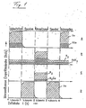
- FIG. 1 shows a diagram of the mass flow modulation for the growth of Se-doped GaAs.
- curve A represents the mass flow diagram of a mixture of an organometallic gallium compound (OGa), e.g. B. DEGaCl, with helium (He) as the carrier gas
- curve B is the mass flow diagram of a mixture of arsine (AsH3) and hydrogen (H2) as the carrier gas
- curve C is the mass flow diagram of a mixture of one Dopant (Do), e.g. B. H2Se, and hydrogen (H2) as the carrier gas
- curve D the mass flow diagram of the purge gas (He).
- Helium which also serves as a carrier gas for the organometallic metal compound, is used as the purge gas.
- the organometallic gallium compound is metered in via its vapor pressure.
- helium is passed through a thermostated bubble counter, which contains the liquid organometallic compound.
- p-type dopants can be added in the same way.
- AsH3 / H2 mixture for the mass flow of curve B a commercially available mixture of z. B. 10 vol .-% AsH3 can be used in H2.
- This mixture is fed continuously, in the third step of the AsH3 implementation with maximum mass flow and otherwise to a value of z. B. throttled 3% of the maximum mass flow.
- the helium for flushing or flooding during the second and fourth steps of each cycle comes from a corresponding gas bomb.
- the pressure in the chamber during the atomic layer epitaxial growth is preferably 10 to 10,000 Pa (0.1 to 100 mbar) in all steps if a flushing gas is used. If instead of supplying a purge gas between the alternate supply of the connections of the elements, the pressure is reduced by a factor of 100 to 10,000 in the evacuation step. That is, e.g. B. at a chamber pressure of 100 Pa during the alternate supply of the compounds, the pressure on z. B. 0.1 Pa in the evacuation step in between.
- a device or a reactor for producing semiconductor thin films by atomic layer epitaxy growth is also provided, with which the semiconductor thin films with high uniformity can be obtained.
- the reactor according to the invention is particularly suitable for carrying out the process according to the invention.
- FIG. 2 schematically shows a longitudinal section through the reactor.
- a cylinder 1 is provided at the upper end with a funnel-shaped hood 2 which tapers from its base 3, that is to say its lower end connected to the cylinder 1, to its upper end, at which the gas inlet 4 is located.
- the gas inlet 4 is arranged radially offset from the cylinder axis 5 of the chamber.
- the funnel axis 6 of the hood 2 forms an angle ⁇ with the cylinder axis 5 of the chamber which is greater than 0 and less than 90 °, generally 20 to 70 °, preferably 40 to 60 °.
- the substrate 7 is arranged in a radial plane to the cylinder axis 5, on which the semiconductor thin layer is to be formed by atomic layer epitaxy growth.
- the substrate is held by a substrate holder 8.
- the substrate holder 8 consists of a cylindrical section 9 which is coaxial with the cylinder axis 5 and an annular flange 10 which extends inwards to the cylinder axis 5 via a rounded edge and on which the substrate 7 rests.
- the substrate holder 8 is rotatably mounted on a base plate 11 about the cylinder axis 5.
- a roller or ball bearing 12 is provided between the lower end of the cylindrical section 9 of the substrate holder 8 and the base plate 11.
- the lower end of the reaction chamber 1 sits on a container 13 in which the base plate 11 is also fastened, the container 13 being connected to a vacuum pump (not shown).
- the gas flowing into the reaction chamber from the inlet 4 strikes the substrate 7 obliquely.
- the substrate 7 obliquely.
- the substrate 7 Due to the oblique arrangement of the funnel axis 6 with respect to the cylinder axis 5 and thus the main flow direction of the gases, the substrate 7 is namely arranged obliquely to the main flow direction of the gases. This leads to a compression of the gases in the area 17 of the hood 2 above the substrate 7, which is opposite the gas inlet 4, and thus to a uniform depletion of the gases.
- the inclined design of the hood 2 means that its internal volume and thus the gas volume in the reactor are low. This has the consequence that the amount of the sometimes very toxic compounds of the semiconductor elements, which are alternately supplied to the reaction chamber consisting of hood 2 and cylinder 1, is relatively small is and that the gas exchange, ie the suction of the gases from the hood 2 via the annular gap 18 between the cylindrical portion 9 of the holder 8 and the inner wall of the cylinder 1 of the reaction chamber can be carried out quickly.
- the annular gap 18 can also be made relatively narrow. The consequence of this is that the substrate holder 8 can be made rotatable as a turbine impeller, the blades or other gas-directing elements of the turbine impeller or the substrate holder 8 not shown in the drawing being arranged in the annular gap 18.
- the substrate holder 8 By designing the substrate holder 8 as a turbine impeller, no bushings, cables and the like which impair the vacuum in the container 13 or a motor for driving the substrate holder 8 in the container 13 with corresponding particle abrasion are required.
- the device according to the invention is aerodynamically designed, ie gas turbulence can be avoided.
- the hood 2 and optionally the cylinder 1 of the reaction chamber are coated on the inside with silicon nitride (Si3N4).
- the substrate holder 8 and optionally the bearing 12 and the base plate 11 can consist of Si3N4 ceramic or be coated with it.
- silicon nitride has a very low adhesive coefficient for arsine, phosphine and organometallic gallium compounds, in particular DEGaCl, so that there is a risk that residues of arsine, phosphine or the organometallic compound, even after the rinsing cycle, still on the substrate holder 8 adhere and lead to the formation of precipitates on the substrate holder 8 or to gas phase reactions during the subsequent supply of the organometallic gallium compound or of arsine or phosphine, is further eliminated.
- the heating element 14 is also preferably designed as a graphite resistor coated with silicon nitride.
Applications Claiming Priority (2)
| Application Number | Priority Date | Filing Date | Title |
|---|---|---|---|
| DE3743938A DE3743938C2 (de) | 1987-12-23 | 1987-12-23 | Verfahren zum Atomschicht-Epitaxie-Aufwachsen einer III/V-Verbindungshalbleiter-Dünnschicht |
| DE3743938 | 1987-12-23 |
Publications (3)
| Publication Number | Publication Date |
|---|---|
| EP0321909A2 true EP0321909A2 (fr) | 1989-06-28 |
| EP0321909A3 EP0321909A3 (fr) | 1991-07-24 |
| EP0321909B1 EP0321909B1 (fr) | 1993-12-01 |
Family
ID=6343501
Family Applications (1)
| Application Number | Title | Priority Date | Filing Date |
|---|---|---|---|
| EP88121243A Expired - Lifetime EP0321909B1 (fr) | 1987-12-23 | 1988-12-19 | Procédé et appareillage pour l'épitaxie par couches monoatomiques |
Country Status (4)
| Country | Link |
|---|---|
| US (1) | US4993357A (fr) |
| EP (1) | EP0321909B1 (fr) |
| JP (1) | JPH01264993A (fr) |
| DE (2) | DE3743938C2 (fr) |
Families Citing this family (114)
| Publication number | Priority date | Publication date | Assignee | Title |
|---|---|---|---|---|
| US5294286A (en) * | 1984-07-26 | 1994-03-15 | Research Development Corporation Of Japan | Process for forming a thin film of silicon |
| US5225366A (en) * | 1990-06-22 | 1993-07-06 | The United States Of America As Represented By The Secretary Of The Navy | Apparatus for and a method of growing thin films of elemental semiconductors |
| JPH06310438A (ja) * | 1993-04-22 | 1994-11-04 | Mitsubishi Electric Corp | 化合物半導体気相成長用基板ホルダおよび化合物半導体気相成長装置 |
| FI97730C (fi) * | 1994-11-28 | 1997-02-10 | Mikrokemia Oy | Laitteisto ohutkalvojen valmistamiseksi |
| FI97731C (fi) * | 1994-11-28 | 1997-02-10 | Mikrokemia Oy | Menetelmä ja laite ohutkalvojen valmistamiseksi |
| FI100409B (fi) | 1994-11-28 | 1997-11-28 | Asm Int | Menetelmä ja laitteisto ohutkalvojen valmistamiseksi |
| US6342277B1 (en) | 1996-08-16 | 2002-01-29 | Licensee For Microelectronics: Asm America, Inc. | Sequential chemical vapor deposition |
| US5916365A (en) * | 1996-08-16 | 1999-06-29 | Sherman; Arthur | Sequential chemical vapor deposition |
| US6671223B2 (en) * | 1996-12-20 | 2003-12-30 | Westerngeco, L.L.C. | Control devices for controlling the position of a marine seismic streamer |
| TW460943B (en) * | 1997-06-11 | 2001-10-21 | Applied Materials Inc | Reduction of mobile ion and metal contamination in HDP-CVD chambers using chamber seasoning film depositions |
| DE19845252A1 (de) * | 1998-10-01 | 2000-04-06 | Deutsche Telekom Ag | Verfahren zur Herstellung von Halbleiterschichten |
| FI118342B (fi) | 1999-05-10 | 2007-10-15 | Asm Int | Laite ohutkalvojen valmistamiseksi |
| US6812157B1 (en) | 1999-06-24 | 2004-11-02 | Prasad Narhar Gadgil | Apparatus for atomic layer chemical vapor deposition |
| US6620723B1 (en) | 2000-06-27 | 2003-09-16 | Applied Materials, Inc. | Formation of boride barrier layers using chemisorption techniques |
| US7964505B2 (en) * | 2005-01-19 | 2011-06-21 | Applied Materials, Inc. | Atomic layer deposition of tungsten materials |
| US6551929B1 (en) * | 2000-06-28 | 2003-04-22 | Applied Materials, Inc. | Bifurcated deposition process for depositing refractory metal layers employing atomic layer deposition and chemical vapor deposition techniques |
| US7732327B2 (en) | 2000-06-28 | 2010-06-08 | Applied Materials, Inc. | Vapor deposition of tungsten materials |
| US7405158B2 (en) | 2000-06-28 | 2008-07-29 | Applied Materials, Inc. | Methods for depositing tungsten layers employing atomic layer deposition techniques |
| US7101795B1 (en) | 2000-06-28 | 2006-09-05 | Applied Materials, Inc. | Method and apparatus for depositing refractory metal layers employing sequential deposition techniques to form a nucleation layer |
| US6765178B2 (en) | 2000-12-29 | 2004-07-20 | Applied Materials, Inc. | Chamber for uniform substrate heating |
| US6998579B2 (en) | 2000-12-29 | 2006-02-14 | Applied Materials, Inc. | Chamber for uniform substrate heating |
| US6825447B2 (en) | 2000-12-29 | 2004-11-30 | Applied Materials, Inc. | Apparatus and method for uniform substrate heating and contaminate collection |
| US20020083897A1 (en) * | 2000-12-29 | 2002-07-04 | Applied Materials, Inc. | Full glass substrate deposition in plasma enhanced chemical vapor deposition |
| US6811814B2 (en) | 2001-01-16 | 2004-11-02 | Applied Materials, Inc. | Method for growing thin films by catalytic enhancement |
| US20020127336A1 (en) * | 2001-01-16 | 2002-09-12 | Applied Materials, Inc. | Method for growing thin films by catalytic enhancement |
| US6951804B2 (en) * | 2001-02-02 | 2005-10-04 | Applied Materials, Inc. | Formation of a tantalum-nitride layer |
| US6878206B2 (en) | 2001-07-16 | 2005-04-12 | Applied Materials, Inc. | Lid assembly for a processing system to facilitate sequential deposition techniques |
| US6660126B2 (en) | 2001-03-02 | 2003-12-09 | Applied Materials, Inc. | Lid assembly for a processing system to facilitate sequential deposition techniques |
| US6939579B2 (en) * | 2001-03-07 | 2005-09-06 | Asm International N.V. | ALD reactor and method with controlled wall temperature |
| US6734020B2 (en) | 2001-03-07 | 2004-05-11 | Applied Materials, Inc. | Valve control system for atomic layer deposition chamber |
| US6849545B2 (en) | 2001-06-20 | 2005-02-01 | Applied Materials, Inc. | System and method to form a composite film stack utilizing sequential deposition techniques |
| US20070009658A1 (en) * | 2001-07-13 | 2007-01-11 | Yoo Jong H | Pulse nucleation enhanced nucleation technique for improved step coverage and better gap fill for WCVD process |
| US7211144B2 (en) * | 2001-07-13 | 2007-05-01 | Applied Materials, Inc. | Pulsed nucleation deposition of tungsten layers |
| US20030029715A1 (en) * | 2001-07-25 | 2003-02-13 | Applied Materials, Inc. | An Apparatus For Annealing Substrates In Physical Vapor Deposition Systems |
| US20090004850A1 (en) * | 2001-07-25 | 2009-01-01 | Seshadri Ganguli | Process for forming cobalt and cobalt silicide materials in tungsten contact applications |
| US8110489B2 (en) * | 2001-07-25 | 2012-02-07 | Applied Materials, Inc. | Process for forming cobalt-containing materials |
| US20080268635A1 (en) * | 2001-07-25 | 2008-10-30 | Sang-Ho Yu | Process for forming cobalt and cobalt silicide materials in copper contact applications |
| JP2005504885A (ja) | 2001-07-25 | 2005-02-17 | アプライド マテリアルズ インコーポレイテッド | 新規なスパッタ堆積方法を使用したバリア形成 |
| US9051641B2 (en) * | 2001-07-25 | 2015-06-09 | Applied Materials, Inc. | Cobalt deposition on barrier surfaces |
| US7085616B2 (en) * | 2001-07-27 | 2006-08-01 | Applied Materials, Inc. | Atomic layer deposition apparatus |
| US6718126B2 (en) | 2001-09-14 | 2004-04-06 | Applied Materials, Inc. | Apparatus and method for vaporizing solid precursor for CVD or atomic layer deposition |
| US20030059538A1 (en) * | 2001-09-26 | 2003-03-27 | Applied Materials, Inc. | Integration of barrier layer and seed layer |
| US7049226B2 (en) | 2001-09-26 | 2006-05-23 | Applied Materials, Inc. | Integration of ALD tantalum nitride for copper metallization |
| US6936906B2 (en) * | 2001-09-26 | 2005-08-30 | Applied Materials, Inc. | Integration of barrier layer and seed layer |
| US7204886B2 (en) * | 2002-11-14 | 2007-04-17 | Applied Materials, Inc. | Apparatus and method for hybrid chemical processing |
| US6916398B2 (en) * | 2001-10-26 | 2005-07-12 | Applied Materials, Inc. | Gas delivery apparatus and method for atomic layer deposition |
| US7780785B2 (en) | 2001-10-26 | 2010-08-24 | Applied Materials, Inc. | Gas delivery apparatus for atomic layer deposition |
| US6773507B2 (en) * | 2001-12-06 | 2004-08-10 | Applied Materials, Inc. | Apparatus and method for fast-cycle atomic layer deposition |
| US6729824B2 (en) | 2001-12-14 | 2004-05-04 | Applied Materials, Inc. | Dual robot processing system |
| CN1643179B (zh) * | 2002-01-17 | 2010-05-26 | 松德沃技术公司 | Ald装置和方法 |
| US7175713B2 (en) | 2002-01-25 | 2007-02-13 | Applied Materials, Inc. | Apparatus for cyclical deposition of thin films |
| US6998014B2 (en) * | 2002-01-26 | 2006-02-14 | Applied Materials, Inc. | Apparatus and method for plasma assisted deposition |
| US6911391B2 (en) * | 2002-01-26 | 2005-06-28 | Applied Materials, Inc. | Integration of titanium and titanium nitride layers |
| US6866746B2 (en) * | 2002-01-26 | 2005-03-15 | Applied Materials, Inc. | Clamshell and small volume chamber with fixed substrate support |
| US6827978B2 (en) * | 2002-02-11 | 2004-12-07 | Applied Materials, Inc. | Deposition of tungsten films |
| US6833161B2 (en) * | 2002-02-26 | 2004-12-21 | Applied Materials, Inc. | Cyclical deposition of tungsten nitride for metal oxide gate electrode |
| US6972267B2 (en) * | 2002-03-04 | 2005-12-06 | Applied Materials, Inc. | Sequential deposition of tantalum nitride using a tantalum-containing precursor and a nitrogen-containing precursor |
| US7250083B2 (en) * | 2002-03-08 | 2007-07-31 | Sundew Technologies, Llc | ALD method and apparatus |
| US7439191B2 (en) * | 2002-04-05 | 2008-10-21 | Applied Materials, Inc. | Deposition of silicon layers for active matrix liquid crystal display (AMLCD) applications |
| US6720027B2 (en) | 2002-04-08 | 2004-04-13 | Applied Materials, Inc. | Cyclical deposition of a variable content titanium silicon nitride layer |
| US6846516B2 (en) * | 2002-04-08 | 2005-01-25 | Applied Materials, Inc. | Multiple precursor cyclical deposition system |
| US20030194825A1 (en) * | 2002-04-10 | 2003-10-16 | Kam Law | Deposition of gate metallization for active matrix liquid crystal display (AMLCD) applications |
| US6869838B2 (en) * | 2002-04-09 | 2005-03-22 | Applied Materials, Inc. | Deposition of passivation layers for active matrix liquid crystal display (AMLCD) applications |
| US6875271B2 (en) | 2002-04-09 | 2005-04-05 | Applied Materials, Inc. | Simultaneous cyclical deposition in different processing regions |
| US7279432B2 (en) | 2002-04-16 | 2007-10-09 | Applied Materials, Inc. | System and method for forming an integrated barrier layer |
| US7186385B2 (en) * | 2002-07-17 | 2007-03-06 | Applied Materials, Inc. | Apparatus for providing gas to a processing chamber |
| US6955211B2 (en) | 2002-07-17 | 2005-10-18 | Applied Materials, Inc. | Method and apparatus for gas temperature control in a semiconductor processing system |
| US7066194B2 (en) * | 2002-07-19 | 2006-06-27 | Applied Materials, Inc. | Valve design and configuration for fast delivery system |
| US6772072B2 (en) | 2002-07-22 | 2004-08-03 | Applied Materials, Inc. | Method and apparatus for monitoring solid precursor delivery |
| US6915592B2 (en) * | 2002-07-29 | 2005-07-12 | Applied Materials, Inc. | Method and apparatus for generating gas to a processing chamber |
| US6821563B2 (en) | 2002-10-02 | 2004-11-23 | Applied Materials, Inc. | Gas distribution system for cyclical layer deposition |
| US20040065255A1 (en) * | 2002-10-02 | 2004-04-08 | Applied Materials, Inc. | Cyclical layer deposition system |
| US20040069227A1 (en) * | 2002-10-09 | 2004-04-15 | Applied Materials, Inc. | Processing chamber configured for uniform gas flow |
| US6905737B2 (en) * | 2002-10-11 | 2005-06-14 | Applied Materials, Inc. | Method of delivering activated species for rapid cyclical deposition |
| US7262133B2 (en) | 2003-01-07 | 2007-08-28 | Applied Materials, Inc. | Enhancement of copper line reliability using thin ALD tan film to cap the copper line |
| JP4528489B2 (ja) * | 2003-01-27 | 2010-08-18 | 独立行政法人理化学研究所 | p型半導体を用いた紫外発光素子 |
| US6868859B2 (en) * | 2003-01-29 | 2005-03-22 | Applied Materials, Inc. | Rotary gas valve for pulsing a gas |
| US6994319B2 (en) * | 2003-01-29 | 2006-02-07 | Applied Materials, Inc. | Membrane gas valve for pulsing a gas |
| US20040177813A1 (en) | 2003-03-12 | 2004-09-16 | Applied Materials, Inc. | Substrate support lift mechanism |
| US7342984B1 (en) | 2003-04-03 | 2008-03-11 | Zilog, Inc. | Counting clock cycles over the duration of a first character and using a remainder value to determine when to sample a bit of a second character |
| US20040198069A1 (en) | 2003-04-04 | 2004-10-07 | Applied Materials, Inc. | Method for hafnium nitride deposition |
| KR20060079144A (ko) * | 2003-06-18 | 2006-07-05 | 어플라이드 머티어리얼스, 인코포레이티드 | 배리어 물질의 원자층 증착 |
| WO2005003406A2 (fr) * | 2003-06-27 | 2005-01-13 | Sundew Technologies, Llc | Procede et dispositif ameliores pour le depot par couche atomique (ald) |
| US20100129548A1 (en) * | 2003-06-27 | 2010-05-27 | Sundew Technologies, Llc | Ald apparatus and method |
| US20050067103A1 (en) * | 2003-09-26 | 2005-03-31 | Applied Materials, Inc. | Interferometer endpoint monitoring device |
| US20050095859A1 (en) * | 2003-11-03 | 2005-05-05 | Applied Materials, Inc. | Precursor delivery system with rate control |
| US20050252449A1 (en) * | 2004-05-12 | 2005-11-17 | Nguyen Son T | Control of gas flow and delivery to suppress the formation of particles in an MOCVD/ALD system |
| US20060153995A1 (en) * | 2004-05-21 | 2006-07-13 | Applied Materials, Inc. | Method for fabricating a dielectric stack |
| US8323754B2 (en) * | 2004-05-21 | 2012-12-04 | Applied Materials, Inc. | Stabilization of high-k dielectric materials |
| US20060019033A1 (en) * | 2004-05-21 | 2006-01-26 | Applied Materials, Inc. | Plasma treatment of hafnium-containing materials |
| US8119210B2 (en) * | 2004-05-21 | 2012-02-21 | Applied Materials, Inc. | Formation of a silicon oxynitride layer on a high-k dielectric material |
| KR100597322B1 (ko) * | 2005-03-16 | 2006-07-06 | 주식회사 아이피에스 | 박막증착방법 |
| US20070020890A1 (en) * | 2005-07-19 | 2007-01-25 | Applied Materials, Inc. | Method and apparatus for semiconductor processing |
| US20070049043A1 (en) * | 2005-08-23 | 2007-03-01 | Applied Materials, Inc. | Nitrogen profile engineering in HI-K nitridation for device performance enhancement and reliability improvement |
| US7402534B2 (en) * | 2005-08-26 | 2008-07-22 | Applied Materials, Inc. | Pretreatment processes within a batch ALD reactor |
| US20070065578A1 (en) * | 2005-09-21 | 2007-03-22 | Applied Materials, Inc. | Treatment processes for a batch ALD reactor |
| US7464917B2 (en) * | 2005-10-07 | 2008-12-16 | Appiled Materials, Inc. | Ampoule splash guard apparatus |
| TW200737307A (en) * | 2005-11-04 | 2007-10-01 | Applied Materials Inc | Apparatus and process for plasma-enhanced atomic layer deposition |
| US20070252299A1 (en) * | 2006-04-27 | 2007-11-01 | Applied Materials, Inc. | Synchronization of precursor pulsing and wafer rotation |
| US7798096B2 (en) * | 2006-05-05 | 2010-09-21 | Applied Materials, Inc. | Plasma, UV and ion/neutral assisted ALD or CVD in a batch tool |
| US20070259111A1 (en) * | 2006-05-05 | 2007-11-08 | Singh Kaushal K | Method and apparatus for photo-excitation of chemicals for atomic layer deposition of dielectric film |
| US7601648B2 (en) | 2006-07-31 | 2009-10-13 | Applied Materials, Inc. | Method for fabricating an integrated gate dielectric layer for field effect transistors |
| US20080099436A1 (en) * | 2006-10-30 | 2008-05-01 | Michael Grimbergen | Endpoint detection for photomask etching |
| US8158526B2 (en) | 2006-10-30 | 2012-04-17 | Applied Materials, Inc. | Endpoint detection for photomask etching |
| US7775508B2 (en) * | 2006-10-31 | 2010-08-17 | Applied Materials, Inc. | Ampoule for liquid draw and vapor draw with a continuous level sensor |
| US20080206987A1 (en) * | 2007-01-29 | 2008-08-28 | Gelatos Avgerinos V | Process for tungsten nitride deposition by a temperature controlled lid assembly |
| US8146896B2 (en) * | 2008-10-31 | 2012-04-03 | Applied Materials, Inc. | Chemical precursor ampoule for vapor deposition processes |
| DE102008059125A1 (de) * | 2008-11-26 | 2010-05-27 | Air Liquide Deutschland Gmbh | Verfahren und Vorrichtung zur Funktionalisierung eines Zielbereiches einer Oberfläche |
| US8778204B2 (en) | 2010-10-29 | 2014-07-15 | Applied Materials, Inc. | Methods for reducing photoresist interference when monitoring a target layer in a plasma process |
| US8961804B2 (en) | 2011-10-25 | 2015-02-24 | Applied Materials, Inc. | Etch rate detection for photomask etching |
| US8808559B2 (en) | 2011-11-22 | 2014-08-19 | Applied Materials, Inc. | Etch rate detection for reflective multi-material layers etching |
| US8900469B2 (en) | 2011-12-19 | 2014-12-02 | Applied Materials, Inc. | Etch rate detection for anti-reflective coating layer and absorber layer etching |
| US9805939B2 (en) | 2012-10-12 | 2017-10-31 | Applied Materials, Inc. | Dual endpoint detection for advanced phase shift and binary photomasks |
| US8778574B2 (en) | 2012-11-30 | 2014-07-15 | Applied Materials, Inc. | Method for etching EUV material layers utilized to form a photomask |
Citations (4)
| Publication number | Priority date | Publication date | Assignee | Title |
|---|---|---|---|---|
| EP0015390A1 (fr) * | 1979-02-28 | 1980-09-17 | Oy Lohja Ab | Méthode et appareil pour réaliser la croissance de films minces d'un composé |
| EP0068839A1 (fr) * | 1981-06-29 | 1983-01-05 | Fujitsu Limited | Procédé et appareil pour la croissance d'un semiconducteur à partir de la phase gazeuse |
| JPS6287485A (ja) * | 1985-10-11 | 1987-04-21 | Nec Corp | 気相エピタキシヤル成長方法 |
| JPH06287485A (ja) * | 1993-04-06 | 1994-10-11 | Nissan Motor Co Ltd | 摺動部用に適した電着塗料 |
Family Cites Families (7)
| Publication number | Priority date | Publication date | Assignee | Title |
|---|---|---|---|---|
| SE393967B (sv) * | 1974-11-29 | 1977-05-31 | Sateko Oy | Forfarande och for utforande av stroleggning mellan lagren i ett virkespaket |
| JPS5828827A (ja) * | 1981-08-12 | 1983-02-19 | Matsushita Electric Ind Co Ltd | 化学気相堆積膜形成装置 |
| JPS58158914A (ja) * | 1982-03-16 | 1983-09-21 | Semiconductor Res Found | 半導体製造装置 |
| JPS5923513A (ja) * | 1982-07-30 | 1984-02-07 | Hitachi Ltd | 反応炉 |
| JPH0766910B2 (ja) * | 1984-07-26 | 1995-07-19 | 新技術事業団 | 半導体単結晶成長装置 |
| JPS62158877A (ja) * | 1986-01-07 | 1987-07-14 | Hitachi Electronics Eng Co Ltd | Cvd薄膜形成装置 |
| JPS62238365A (ja) * | 1986-04-08 | 1987-10-19 | Hitachi Electronics Eng Co Ltd | Cvd薄膜形成装置 |
-
1987
- 1987-12-23 DE DE3743938A patent/DE3743938C2/de not_active Expired - Fee Related
-
1988
- 1988-12-19 DE DE88121243T patent/DE3886023D1/de not_active Expired - Fee Related
- 1988-12-19 JP JP63318717A patent/JPH01264993A/ja active Pending
- 1988-12-19 EP EP88121243A patent/EP0321909B1/fr not_active Expired - Lifetime
- 1988-12-21 US US07/287,903 patent/US4993357A/en not_active Expired - Fee Related
Patent Citations (4)
| Publication number | Priority date | Publication date | Assignee | Title |
|---|---|---|---|---|
| EP0015390A1 (fr) * | 1979-02-28 | 1980-09-17 | Oy Lohja Ab | Méthode et appareil pour réaliser la croissance de films minces d'un composé |
| EP0068839A1 (fr) * | 1981-06-29 | 1983-01-05 | Fujitsu Limited | Procédé et appareil pour la croissance d'un semiconducteur à partir de la phase gazeuse |
| JPS6287485A (ja) * | 1985-10-11 | 1987-04-21 | Nec Corp | 気相エピタキシヤル成長方法 |
| JPH06287485A (ja) * | 1993-04-06 | 1994-10-11 | Nissan Motor Co Ltd | 摺動部用に適した電着塗料 |
Non-Patent Citations (1)
| Title |
|---|
| EXTENDED ABSTRACTS OF THE 19TH CONFERENCE ON SOLID STATE DEVICES AND MATERIALS, Tokyo, 25. - 27. August 1987, Seiten 475-478; M. OZEKI et al.: "Growth of AlGaAs by atomic layer epitaxy using a pulsed vapor phase method" * |
Also Published As
| Publication number | Publication date |
|---|---|
| EP0321909B1 (fr) | 1993-12-01 |
| DE3743938A1 (de) | 1989-07-13 |
| US4993357A (en) | 1991-02-19 |
| EP0321909A3 (fr) | 1991-07-24 |
| DE3743938C2 (de) | 1995-08-31 |
| DE3886023D1 (de) | 1994-01-13 |
| JPH01264993A (ja) | 1989-10-23 |
Similar Documents
| Publication | Publication Date | Title |
|---|---|---|
| EP0321909B1 (fr) | Procédé et appareillage pour l'épitaxie par couches monoatomiques | |
| DE60121768T2 (de) | Verfahren zur herstellung eines halbleiterbauelements mit nitridzusammensetzung der gruppe iii | |
| DE4404110C2 (de) | Substrathalter für die metallorganische chemische Dampfabscheidung | |
| DE2214404C3 (de) | Verfahren zum Herstellen epitaktischer Dünnschichten im Molekularstrahl-Epitaxieverfahren | |
| DE3526825C2 (fr) | ||
| DE4138121C2 (de) | Verfahren zur Herstellung einer Solarzelle | |
| DE69631662T2 (de) | GaAs-SUBSTRAT MIT GRADIERT ZUSAMMENGESETZTEM AeGaAsSb-PUFFER ZUR HERSTELLUNG VON FELDEFFEKTTRANSISTOREN MIT HOHEM INDIUM-GEHALT | |
| DE10392313T5 (de) | Auf Galliumnitrid basierende Vorrichtungen und Herstellungsverfahren | |
| DE102011079855A1 (de) | Siliciumcarbideinkristall und Verfahren zu dessen Herstellung | |
| DE2830081A1 (de) | Verfahren zum herstellen eines halbleitermateriales der gruppen iii/v des periodischen systems | |
| DE1444514B2 (de) | Verfahren zur herstellung eines epitaktisch auf ein einkristallines substrat aufgewachsenen filmes aus halbleiterverbindungen | |
| DE2231926B2 (de) | Verfahren zur Herstellung von Halbleitermaterial | |
| DE2715558A1 (de) | Verfahren zur herstellung eines bauteils zur verwendung bei der halbleiterbauelementfertigung | |
| DE60112372T2 (de) | Vorrichtung und Verfahren zur chemischen Gasphasenabscheidung | |
| DE3526824C2 (fr) | ||
| DE112018002713T5 (de) | SiC-EPITAXIE-WAFER UND VERFAHREN ZU DESSEN HERSTELLUNG | |
| EP2024991A1 (fr) | Procédés de fabrication d'un cristal massif dopé au iii-n et d'un substrat libre dopé au iii-n et cristal massif dopé au iii-n et substrat libre dopé au iii-n | |
| DE10009876B4 (de) | Verfahren zum Bilden eines einkristallinen Films | |
| DE2529747C3 (de) | Verfahren zur Erzeugung von epitaktischen Aufwachsungen aus der flussigen Phase | |
| DE112019003770T5 (de) | Fotosensitive Vorrichtung und Verfahren für deren Herstellung | |
| DE3526889A1 (de) | Einrichtung zum bilden eines halbleiterkristalls | |
| DE112018002163T5 (de) | Verfahren zur Herstellung eines Silicium-Einkristalls, Verfahren zur Herstellung eines epitaktischen Silicium-Wafers, Silicium-Einkristall, und epitaktischer Silicium-Wafer | |
| DE4222406A1 (de) | Verfahren zur herstellung von diamantschichten durch dampfphasensynthese | |
| DE10011876A1 (de) | III-V-Verbundhalbleiter | |
| DE1544292C3 (de) | Verfahren zum Herstellen stabförmiger Siliciumeinkristalle mit über die gesamte Stablänge homogener Antimondotierung |
Legal Events
| Date | Code | Title | Description |
|---|---|---|---|
| PUAI | Public reference made under article 153(3) epc to a published international application that has entered the european phase |
Free format text: ORIGINAL CODE: 0009012 |
|
| AK | Designated contracting states |
Kind code of ref document: A2 Designated state(s): CH DE FR GB IT LI NL SE |
|
| PUAL | Search report despatched |
Free format text: ORIGINAL CODE: 0009013 |
|
| AK | Designated contracting states |
Kind code of ref document: A3 Designated state(s): CH DE FR GB IT LI NL SE |
|
| 17P | Request for examination filed |
Effective date: 19911220 |
|
| 17Q | First examination report despatched |
Effective date: 19921009 |
|
| GRAA | (expected) grant |
Free format text: ORIGINAL CODE: 0009210 |
|
| AK | Designated contracting states |
Kind code of ref document: B1 Designated state(s): CH DE FR GB IT LI NL SE |
|
| PG25 | Lapsed in a contracting state [announced via postgrant information from national office to epo] |
Ref country code: NL Effective date: 19931201 Ref country code: SE Effective date: 19931201 Ref country code: IT Free format text: LAPSE BECAUSE OF FAILURE TO SUBMIT A TRANSLATION OF THE DESCRIPTION OR TO PAY THE FEE WITHIN THE PRE;WARNING: LAPSES OF ITALIAN PATENTS WITH EFFECTIVE DATE BEFORE 2007 MAY HAVE OCCURRED AT ANY TIME BEFORE 2007. THE CORRECT EFFECTIVE DATE MAY BE DIFFERENT FROM THE ONE RECORDED.SCRIBED TIME-LIMIT Effective date: 19931201 |
|
| REF | Corresponds to: |
Ref document number: 3886023 Country of ref document: DE Date of ref document: 19940113 |
|
| GBT | Gb: translation of ep patent filed (gb section 77(6)(a)/1977) |
Effective date: 19940126 |
|
| ET | Fr: translation filed | ||
| NLV1 | Nl: lapsed or annulled due to failure to fulfill the requirements of art. 29p and 29m of the patents act | ||
| PLBE | No opposition filed within time limit |
Free format text: ORIGINAL CODE: 0009261 |
|
| STAA | Information on the status of an ep patent application or granted ep patent |
Free format text: STATUS: NO OPPOSITION FILED WITHIN TIME LIMIT |
|
| 26N | No opposition filed | ||
| PGFP | Annual fee paid to national office [announced via postgrant information from national office to epo] |
Ref country code: GB Payment date: 19941209 Year of fee payment: 7 |
|
| PGFP | Annual fee paid to national office [announced via postgrant information from national office to epo] |
Ref country code: FR Payment date: 19941215 Year of fee payment: 7 |
|
| PGFP | Annual fee paid to national office [announced via postgrant information from national office to epo] |
Ref country code: CH Payment date: 19941221 Year of fee payment: 7 |
|
| PGFP | Annual fee paid to national office [announced via postgrant information from national office to epo] |
Ref country code: DE Payment date: 19950216 Year of fee payment: 7 |
|
| PG25 | Lapsed in a contracting state [announced via postgrant information from national office to epo] |
Ref country code: GB Effective date: 19951219 |
|
| PG25 | Lapsed in a contracting state [announced via postgrant information from national office to epo] |
Ref country code: LI Effective date: 19951231 Ref country code: CH Effective date: 19951231 |
|
| GBPC | Gb: european patent ceased through non-payment of renewal fee |
Effective date: 19951219 |
|
| REG | Reference to a national code |
Ref country code: CH Ref legal event code: PL |
|
| PG25 | Lapsed in a contracting state [announced via postgrant information from national office to epo] |
Ref country code: FR Effective date: 19960830 |
|
| PG25 | Lapsed in a contracting state [announced via postgrant information from national office to epo] |
Ref country code: DE Effective date: 19960903 |
|
| REG | Reference to a national code |
Ref country code: FR Ref legal event code: ST |