EP0299221A2 - Gedruckte Leiterplatte - Google Patents
Gedruckte Leiterplatte Download PDFInfo
- Publication number
- EP0299221A2 EP0299221A2 EP88109621A EP88109621A EP0299221A2 EP 0299221 A2 EP0299221 A2 EP 0299221A2 EP 88109621 A EP88109621 A EP 88109621A EP 88109621 A EP88109621 A EP 88109621A EP 0299221 A2 EP0299221 A2 EP 0299221A2
- Authority
- EP
- European Patent Office
- Prior art keywords
- conductors
- conductor
- printed circuit
- circuit panel
- divergence
- Prior art date
- Legal status (The legal status is an assumption and is not a legal conclusion. Google has not performed a legal analysis and makes no representation as to the accuracy of the status listed.)
- Granted
Links
- 239000004020 conductor Substances 0.000 claims abstract description 141
- 239000000758 substrate Substances 0.000 claims description 32
- 238000000034 method Methods 0.000 claims description 9
- 239000000463 material Substances 0.000 claims description 3
- 239000011248 coating agent Substances 0.000 claims 2
- 238000000576 coating method Methods 0.000 claims 2
- 230000003292 diminished effect Effects 0.000 claims 1
- 230000008901 benefit Effects 0.000 description 4
- 230000009467 reduction Effects 0.000 description 4
- 230000002829 reductive effect Effects 0.000 description 4
- 239000004593 Epoxy Substances 0.000 description 3
- 229910052751 metal Inorganic materials 0.000 description 3
- 239000002184 metal Substances 0.000 description 3
- RYGMFSIKBFXOCR-UHFFFAOYSA-N Copper Chemical compound [Cu] RYGMFSIKBFXOCR-UHFFFAOYSA-N 0.000 description 2
- 239000000654 additive Substances 0.000 description 2
- 230000000996 additive effect Effects 0.000 description 2
- 230000002238 attenuated effect Effects 0.000 description 2
- 238000010276 construction Methods 0.000 description 2
- 229910052802 copper Inorganic materials 0.000 description 2
- 239000010949 copper Substances 0.000 description 2
- 230000003247 decreasing effect Effects 0.000 description 2
- 238000004806 packaging method and process Methods 0.000 description 2
- 230000003071 parasitic effect Effects 0.000 description 2
- 229920000642 polymer Polymers 0.000 description 2
- 230000008569 process Effects 0.000 description 2
- 239000004642 Polyimide Substances 0.000 description 1
- 230000002411 adverse Effects 0.000 description 1
- 229910052782 aluminium Inorganic materials 0.000 description 1
- XAGFODPZIPBFFR-UHFFFAOYSA-N aluminium Chemical compound [Al] XAGFODPZIPBFFR-UHFFFAOYSA-N 0.000 description 1
- 230000009286 beneficial effect Effects 0.000 description 1
- 230000015572 biosynthetic process Effects 0.000 description 1
- 239000000969 carrier Substances 0.000 description 1
- 230000008878 coupling Effects 0.000 description 1
- 238000010168 coupling process Methods 0.000 description 1
- 238000005859 coupling reaction Methods 0.000 description 1
- 238000006880 cross-coupling reaction Methods 0.000 description 1
- 230000000694 effects Effects 0.000 description 1
- 239000003365 glass fiber Substances 0.000 description 1
- 239000012212 insulator Substances 0.000 description 1
- 230000000670 limiting effect Effects 0.000 description 1
- 238000004519 manufacturing process Methods 0.000 description 1
- 230000004048 modification Effects 0.000 description 1
- 238000012986 modification Methods 0.000 description 1
- 231100000989 no adverse effect Toxicity 0.000 description 1
- 229920001721 polyimide Polymers 0.000 description 1
- 238000000926 separation method Methods 0.000 description 1
Images
Classifications
-
- H—ELECTRICITY
- H05—ELECTRIC TECHNIQUES NOT OTHERWISE PROVIDED FOR
- H05K—PRINTED CIRCUITS; CASINGS OR CONSTRUCTIONAL DETAILS OF ELECTRIC APPARATUS; MANUFACTURE OF ASSEMBLAGES OF ELECTRICAL COMPONENTS
- H05K1/00—Printed circuits
- H05K1/02—Details
- H05K1/0213—Electrical arrangements not otherwise provided for
- H05K1/0216—Reduction of cross-talk, noise or electromagnetic interference
- H05K1/0228—Compensation of cross-talk by a mutually correlated lay-out of printed circuit traces, e.g. for compensation of cross-talk in mounted connectors
-
- H—ELECTRICITY
- H01—ELECTRIC ELEMENTS
- H01R—ELECTRICALLY-CONDUCTIVE CONNECTIONS; STRUCTURAL ASSOCIATIONS OF A PLURALITY OF MUTUALLY-INSULATED ELECTRICAL CONNECTING ELEMENTS; COUPLING DEVICES; CURRENT COLLECTORS
- H01R13/00—Details of coupling devices of the kinds covered by groups H01R12/70 or H01R24/00 - H01R33/00
- H01R13/646—Details of coupling devices of the kinds covered by groups H01R12/70 or H01R24/00 - H01R33/00 specially adapted for high-frequency, e.g. structures providing an impedance match or phase match
- H01R13/6461—Means for preventing cross-talk
-
- H—ELECTRICITY
- H01—ELECTRIC ELEMENTS
- H01R—ELECTRICALLY-CONDUCTIVE CONNECTIONS; STRUCTURAL ASSOCIATIONS OF A PLURALITY OF MUTUALLY-INSULATED ELECTRICAL CONNECTING ELEMENTS; COUPLING DEVICES; CURRENT COLLECTORS
- H01R13/00—Details of coupling devices of the kinds covered by groups H01R12/70 or H01R24/00 - H01R33/00
- H01R13/646—Details of coupling devices of the kinds covered by groups H01R12/70 or H01R24/00 - H01R33/00 specially adapted for high-frequency, e.g. structures providing an impedance match or phase match
- H01R13/6473—Impedance matching
- H01R13/6474—Impedance matching by variation of conductive properties, e.g. by dimension variations
-
- H—ELECTRICITY
- H05—ELECTRIC TECHNIQUES NOT OTHERWISE PROVIDED FOR
- H05K—PRINTED CIRCUITS; CASINGS OR CONSTRUCTIONAL DETAILS OF ELECTRIC APPARATUS; MANUFACTURE OF ASSEMBLAGES OF ELECTRICAL COMPONENTS
- H05K1/00—Printed circuits
- H05K1/02—Details
- H05K1/0213—Electrical arrangements not otherwise provided for
- H05K1/0237—High frequency adaptations
- H05K1/0245—Lay-out of balanced signal pairs, e.g. differential lines or twisted lines
-
- H—ELECTRICITY
- H05—ELECTRIC TECHNIQUES NOT OTHERWISE PROVIDED FOR
- H05K—PRINTED CIRCUITS; CASINGS OR CONSTRUCTIONAL DETAILS OF ELECTRIC APPARATUS; MANUFACTURE OF ASSEMBLAGES OF ELECTRICAL COMPONENTS
- H05K2201/00—Indexing scheme relating to printed circuits covered by H05K1/00
- H05K2201/09—Shape and layout
- H05K2201/09209—Shape and layout details of conductors
- H05K2201/09218—Conductive traces
- H05K2201/09236—Parallel layout
-
- H—ELECTRICITY
- H05—ELECTRIC TECHNIQUES NOT OTHERWISE PROVIDED FOR
- H05K—PRINTED CIRCUITS; CASINGS OR CONSTRUCTIONAL DETAILS OF ELECTRIC APPARATUS; MANUFACTURE OF ASSEMBLAGES OF ELECTRICAL COMPONENTS
- H05K2201/00—Indexing scheme relating to printed circuits covered by H05K1/00
- H05K2201/09—Shape and layout
- H05K2201/09209—Shape and layout details of conductors
- H05K2201/09218—Conductive traces
- H05K2201/09263—Meander
-
- H—ELECTRICITY
- H05—ELECTRIC TECHNIQUES NOT OTHERWISE PROVIDED FOR
- H05K—PRINTED CIRCUITS; CASINGS OR CONSTRUCTIONAL DETAILS OF ELECTRIC APPARATUS; MANUFACTURE OF ASSEMBLAGES OF ELECTRICAL COMPONENTS
- H05K2201/00—Indexing scheme relating to printed circuits covered by H05K1/00
- H05K2201/09—Shape and layout
- H05K2201/09209—Shape and layout details of conductors
- H05K2201/09654—Shape and layout details of conductors covering at least two types of conductors provided for in H05K2201/09218 - H05K2201/095
- H05K2201/097—Alternating conductors, e.g. alternating different shaped pads, twisted pairs; Alternating components
-
- Y—GENERAL TAGGING OF NEW TECHNOLOGICAL DEVELOPMENTS; GENERAL TAGGING OF CROSS-SECTIONAL TECHNOLOGIES SPANNING OVER SEVERAL SECTIONS OF THE IPC; TECHNICAL SUBJECTS COVERED BY FORMER USPC CROSS-REFERENCE ART COLLECTIONS [XRACs] AND DIGESTS
- Y10—TECHNICAL SUBJECTS COVERED BY FORMER USPC
- Y10T—TECHNICAL SUBJECTS COVERED BY FORMER US CLASSIFICATION
- Y10T29/00—Metal working
- Y10T29/49—Method of mechanical manufacture
- Y10T29/49002—Electrical device making
- Y10T29/49117—Conductor or circuit manufacturing
- Y10T29/49124—On flat or curved insulated base, e.g., printed circuit, etc.
Definitions
- This invention relates to a printed circuit panel in the conductors of which the coupled noise or cross talk is unusually and severely attenuated.
- the adversely affected conductors lie within a proximity region whose effective radius from an energized conductor varies with signal frequency, parasitic capacitance, inductance, source and termination impedence, dielectric constant, distance to ground and voltage plane, extent of conductor parallelism and other factors. As more conductors are placed within in a volume, the high frequency switching induces voltage levels that can be falsely detected as data, resulting in processing errors. These become particularly troublesome among digital circuits.
- the interval of radial distance between neighboring conductors has a minimum value for a particular acceptable signal-to-noise ratio. This dimension is typically decreased by reducing conductor size to enlarge separation, decreasing dielectric constants of insulators, or placing ground reference planes nearby.
- Multi-layer substrates frequently limit the number of signal planes as opposed to supply planes, to two orthogonally arranged planes adjacent to a ground plane, as in microstrip structure. In a different arrangement, signal planes are grouped in four with conductors on adjacent signal planes orthogonally disposed and the group placed between a pair of ground planes.
- the invention as claimed is intended to remedy this drawback. It solves the problem of providing an printed circuit panel with an arrangement of closely adjacent electrical conductors having an unusually large reduction of coupled noise during energization of the proximate conductors, the arrangement of the conductors permitting denser packaging in multiple layer substrates, but having significantly less cross coupling of signals among conductors when energized particularly in digital pulse circuits.
- the advantages of the invention are attained by providing a substrate for supporting electrical conductors and, for those particular conductors lying within a region of mutual inductance, arranging them in parallel or common substrate channels to either continually or intermittently converge or diverge relative to each other as they progress along their assigned channels.
- Angle magnitude of relative convergence and divergence or skew is that magnitude necessary to restrict or attenuate the induced voltage levels to acceptable signal-to-noise ratios and typically is between six and fifteen degrees.
- This invention has a major advantage of improving performance by severely limiting the magnitude of voltage fluctuations in neighboring conductors induced from an activated or energized conductor.
- the relative convergence and divergence adds conductor length, such signal propagation delay is typically less than 5% and thus negligable and readily acceptable to obtain the beneficial reduction in coupled noise.
- This delay has an advantage of keeping the primary and induced signals out of synchronism.
- the technique of maintaining limited relative convergence and divergence allows conductors, such as printed circuits, to be formed with nearly the density in common use, even with the conductors confined to individual parallel paths or channels on a substrate. Thus, there is little or no adverse effect on wirability.
- the conductor arrangement also lends itself to construction of multiple layer circuit cards and panels and permits the same reduction of coupled noise when conductors are considered in planes taken at various angles through the panels.
- Conductors are formed on their substrates with the known techniques, such as photolithographic additive or subtractive formation or automatic placement of insulated wires.
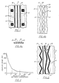
- electrical signal conductors 10, 11 and 12 forming "printed circuits,” are arranged in imaginary channels 13 defined by dashed lines 14 that include necessary spacing and are usually fabricated in close proximity on an insulative substrate 15.
- the substrate may have vias 16 and be a reinforced polymer such as glass fibers in epoxy or polyimide or other suitable material.
- the conductors are frequently copper and are arranged parallel to each other and may be formed by either additive or subtractive processes, or by embedding pre-insulated conductors in a semicured epoxy. They are placed as closely as possible to obtain maximum density but while maintaining a sufficient center-to-center distance to provide an acceptable signal-to-noise ratio for reliable, accurate recognition of changes in signal levels during operation.
- Conductor noise in an unenergized or quiet conductor appears as current disturbances induced from neighboring active conductors undergoing high frequency switching with pulses having fast rise times that produce electromagnetic variations due to parasitic capacitance and inductance.
- the influence primarily results from the frequency and parallel arrangement of the conductors in either the same or different planes, when close enough.
- Fig. 2 where the magnitude of the induced coupled noise voltage is plotted versus the angle of skew or convergence or divergence between a quiet and an active conductor.
- FIG. 3 Examples of several conductor configurations are shown in Fig. 3.
- imaginary assigned conductor channels 13, designated by broken lines 14 are arranged in the usual parallel manner over the surface of substrate 15.
- Each channel is reserved for one of the circuit conductors 17-20 that can be formed of a conductive metal by well-known processes that usually involve lithographic definition and either deposit or removal of metal, such as copper, aluminum or other suitable metal.
- Another technique is to partially embed already insulated conductors in a semicured polymer such as epoxy, then complete the curing.
- Conductors 17-20 are formed during placement on substrate 15 such that there is an absence of parallelism in either convergence or divergence of the longitudinal axis of each conductor relative to those of the remaining conductors within the region of coupled noise.
- the angle ⁇ of convergence or divergence is preferably at least 6 degrees and up to approximately 15 degrees. This arrangement reduces the magnitude of coupled noise or cross talk by an amount of more than 75% of that experienced by continuously parallel conductors.
- a conductor configuration can assume nearly any form within its assigned channel as long as there is the necessary minimum clearance from its neighboring conductors to avoid shorting. Configurations, such as those of conductors 17, 19 and 20, shown in Fig.
- channels 13 carry two insulated conductor pairs 21, 22 and 23, 24 in which the conductors overlie each other in zig-zag fashion on substrate 15.
- These conductors being insulated wires, can be partially embedded in a semicured substrate surface by automatic machine wiring and achieve greater wiring density.
- one wire of a pair can be axially offset along the common channel with respect to the other. Identity of convergence or divergence angles is not necessary.
- cross talk amplitude is still reduced by approximately the same amount because the extent of parallelism of conductor segments is minor.
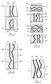
- Figures 5 and 6 illustrate further conductor configurations that are suitable for multiple circuit layers and maintain relative convergence or divergence within the effective cross talk region.
- conductors 25 and 26 on substrate 27 will be assembled with conductors 29 and 30 on substrate 31 to form two circuit planes. Parallel conductors 25 and 30 are assumed to be beyond the influence of cross talk.
- a ground plane can be added either above substrate 27 or below substrate 31.
- Fig. 6 portions of four signal plane layers are shown.
- Conductors 32, 33 and 34 on substrate 35 and conductors 36, 37 and 38 on substrate 39 are oriented generally in the horizontal direction while conductors 42, 43 and 44 on subtrate 45 and conductors 46, 47 and 48 on substrate 49 are oriented generally in the vertical direction.
- the parallel conductors are beyond any substantial influence of coupled noise from each other because of intervening orthogonal layers.
- those in immediate proximity maintain relative convergence or divergence as noted by conductor 33 and its neighbors 32, 34 on either side, and conductors 36 and 38 with respect to conductor 37 and conductors 32 and 34 on the second layer above.
- a ground plane may be added either above substrate 35 or below substrate 49 if desired. It will be noted that in this multi-layer arrangement, only three conductors are parallel in either the horizontal or vertical directions and they are separated into different vertical planes with an intervening signal plane.
- FIG. 7 An alternative conductor arrangement is shown in Fig. 7 where conductors 51, 52 and 53 each converge or diverge within their respective channels 13 on substrate 54 at increasingly greater angles from left to right.
- the angle used by conductor 51 may be six degrees
- conductor 52 may be twelve degrees
- conductor 53 may be eighteen degrees. This pattern can then be repeated.
- each conductor has a straight portion, such as 57a and 58a and a zig-zag portion 57b and 58b, respectively.
- the straight end zig-zag portions for each conductor equals those of the other conductor so that total path lengths are the same. This arrangement retains nonparallel conductors for reduced cross talk.
Landscapes
- Physics & Mathematics (AREA)
- Electromagnetism (AREA)
- Engineering & Computer Science (AREA)
- Microelectronics & Electronic Packaging (AREA)
- Structure Of Printed Boards (AREA)
- Production Of Multi-Layered Print Wiring Board (AREA)
Applications Claiming Priority (2)
| Application Number | Priority Date | Filing Date | Title |
|---|---|---|---|
| US07/072,833 US4785135A (en) | 1987-07-13 | 1987-07-13 | De-coupled printed circuits |
| US72833 | 1993-06-07 |
Publications (3)
| Publication Number | Publication Date |
|---|---|
| EP0299221A2 true EP0299221A2 (de) | 1989-01-18 |
| EP0299221A3 EP0299221A3 (en) | 1990-11-07 |
| EP0299221B1 EP0299221B1 (de) | 1993-04-21 |
Family
ID=22110029
Family Applications (1)
| Application Number | Title | Priority Date | Filing Date |
|---|---|---|---|
| EP88109621A Expired - Lifetime EP0299221B1 (de) | 1987-07-13 | 1988-06-16 | Gedruckte Leiterplatte |
Country Status (4)
| Country | Link |
|---|---|
| US (1) | US4785135A (de) |
| EP (1) | EP0299221B1 (de) |
| JP (1) | JPH0766998B2 (de) |
| DE (1) | DE3880385T2 (de) |
Cited By (1)
| Publication number | Priority date | Publication date | Assignee | Title |
|---|---|---|---|---|
| EP3200567A1 (de) * | 2016-01-25 | 2017-08-02 | Alpine Electronics, Inc. | Verdrahtungsstruktur und gedrucktes verdrahtungssubstrat der verdrahtungsstruktur |
Families Citing this family (39)
| Publication number | Priority date | Publication date | Assignee | Title |
|---|---|---|---|---|
| US4891616A (en) * | 1988-06-01 | 1990-01-02 | Honeywell Inc. | Parallel planar signal transmission system |
| US5186647A (en) | 1992-02-24 | 1993-02-16 | At&T Bell Laboratories | High frequency electrical connector |
| JPH0770837B2 (ja) * | 1992-05-20 | 1995-07-31 | インターナショナル・ビジネス・マシーンズ・コーポレイション | 多層配線を有する電子パッケージ基板及び方法 |
| US5414393A (en) * | 1992-08-20 | 1995-05-09 | Hubbell Incorporated | Telecommunication connector with feedback |
| US5432484A (en) * | 1992-08-20 | 1995-07-11 | Hubbell Incorporated | Connector for communication systems with cancelled crosstalk |
| US5430247A (en) * | 1993-08-31 | 1995-07-04 | Motorola, Inc. | Twisted-pair planar conductor line off-set structure |
| US5917860A (en) * | 1993-12-13 | 1999-06-29 | Industrial Technology Research Institute | Digital transmitter utilizing a phase shifter having decoupled coplanar microstrips |
| US5357051A (en) * | 1994-01-31 | 1994-10-18 | Hwang Richard H | Printed circuit board for reducing radio frequency interferences |
| US5618185A (en) * | 1995-03-15 | 1997-04-08 | Hubbell Incorporated | Crosstalk noise reduction connector for telecommunication system |
| US5817973A (en) * | 1995-06-12 | 1998-10-06 | Berg Technology, Inc. | Low cross talk and impedance controlled electrical cable assembly |
| US6939173B1 (en) | 1995-06-12 | 2005-09-06 | Fci Americas Technology, Inc. | Low cross talk and impedance controlled electrical connector with solder masses |
| TW267265B (en) * | 1995-06-12 | 1996-01-01 | Connector Systems Tech Nv | Low cross talk and impedance controlled electrical connector |
| AU6174196A (en) * | 1995-06-12 | 1997-01-09 | Berg Technology, Inc. | Low cross talk and impedance controlled electrical connector and electrical cable assembly |
| US5789807A (en) * | 1996-10-15 | 1998-08-04 | International Business Machines Corporation | On-chip power distribution for improved decoupling |
| DE19652258A1 (de) * | 1996-12-16 | 1998-06-18 | Ibm | Verbesserte Verdrahtungsstruktur für Hochleistungschips |
| US5931703A (en) * | 1997-02-04 | 1999-08-03 | Hubbell Incorporated | Low crosstalk noise connector for telecommunication systems |
| US5944535A (en) * | 1997-02-04 | 1999-08-31 | Hubbell Incorporated | Interface panel system for networks |
| US7321485B2 (en) | 1997-04-08 | 2008-01-22 | X2Y Attenuators, Llc | Arrangement for energy conditioning |
| US9054094B2 (en) | 1997-04-08 | 2015-06-09 | X2Y Attenuators, Llc | Energy conditioning circuit arrangement for integrated circuit |
| US7336468B2 (en) | 1997-04-08 | 2008-02-26 | X2Y Attenuators, Llc | Arrangement for energy conditioning |
| US6208219B1 (en) * | 1999-05-12 | 2001-03-27 | Samuel Singer | Broadband RF circuits with microstrips laid out in randomly meandering paths |
| US6518663B1 (en) * | 1999-08-30 | 2003-02-11 | Texas Instruments Incorporated | Constant impedance routing for high performance integrated circuit packaging |
| US7271985B1 (en) | 2004-09-24 | 2007-09-18 | Storage Technology Corporation | System and method for crosstalk reduction in a flexible trace interconnect array |
| GB2439862A (en) | 2005-03-01 | 2008-01-09 | X2Y Attenuators Llc | Conditioner with coplanar conductors |
| WO2006106761A1 (ja) * | 2005-03-30 | 2006-10-12 | Matsushita Electric Industrial Co., Ltd. | 伝送線路対 |
| KR101352344B1 (ko) * | 2006-09-13 | 2014-01-15 | 삼성디스플레이 주식회사 | 신호전송 부재 및 이를 갖는 표시장치 |
| JP4979534B2 (ja) * | 2007-10-11 | 2012-07-18 | 日本オプネクスト株式会社 | 光モジュール |
| JP5427644B2 (ja) * | 2010-02-25 | 2014-02-26 | 株式会社日立製作所 | プリント基板 |
| US9930771B2 (en) * | 2015-12-16 | 2018-03-27 | Dell Products, Lp | Aperiodic routing to mitigate floquet mode resonances |
| JP2019005197A (ja) * | 2017-06-23 | 2019-01-17 | 株式会社三共 | 遊技機 |
| JP2019005198A (ja) * | 2017-06-23 | 2019-01-17 | 株式会社三共 | 遊技機 |
| JP2019005199A (ja) * | 2017-06-23 | 2019-01-17 | 株式会社三共 | 遊技機 |
| JP2019017887A (ja) * | 2017-07-21 | 2019-02-07 | 株式会社三共 | 遊技機 |
| JP2019025261A (ja) * | 2017-08-04 | 2019-02-21 | 株式会社三共 | 遊技機 |
| JP2019025263A (ja) * | 2017-08-04 | 2019-02-21 | 株式会社三共 | 遊技機 |
| JP2019107194A (ja) * | 2017-12-18 | 2019-07-04 | 株式会社三共 | 遊技機 |
| JP2019107192A (ja) * | 2017-12-18 | 2019-07-04 | 株式会社三共 | 遊技機 |
| JP6720247B2 (ja) * | 2018-04-26 | 2020-07-08 | 株式会社三共 | 遊技機 |
| US12389531B2 (en) | 2022-03-08 | 2025-08-12 | Murata Manufacturing Co., Ltd. | Circuit module |
Family Cites Families (16)
| Publication number | Priority date | Publication date | Assignee | Title |
|---|---|---|---|---|
| US278289A (en) * | 1883-05-22 | Samuel i | ||
| NL268381A (de) * | 1960-09-28 | |||
| DE1218572B (de) * | 1963-03-22 | 1966-06-08 | Siemens Ag | Fernmeldekabel mit in Lagen angeordneten Einzeladern, aus denen durch gegenseitiges Kreuzen Doppelleitungen gebildet sind |
| FR1402897A (fr) * | 1964-03-06 | 1965-06-18 | Telecommunications Sa | Circuits à conducteurs plats pour câbles de télécommunication |
| US3573670A (en) * | 1969-03-21 | 1971-04-06 | Ibm | High-speed impedance-compensated circuits |
| US3736366A (en) * | 1972-04-27 | 1973-05-29 | Bell Telephone Labor Inc | Mass bonding of twisted pair cables |
| US3761842A (en) * | 1972-06-01 | 1973-09-25 | Bell Telephone Labor Inc | Twisted pair flat conductor cable with means to equalize impedance and propagation velocity |
| US3764727A (en) * | 1972-06-12 | 1973-10-09 | Western Electric Co | Electrically conductive flat cable structures |
| US3774123A (en) * | 1972-12-11 | 1973-11-20 | Ibm | Broad band microstrip n-pole m-throw pin diode switch having predetermined spacing between pole and throw conductors |
| US3876964A (en) * | 1973-08-23 | 1975-04-08 | Amp Inc | Flat flexible transmission cable |
| FR2243578B1 (de) * | 1973-09-12 | 1976-11-19 | Honeywell Bull Soc Ind | |
| GB1589519A (en) * | 1976-11-19 | 1981-05-13 | Solartron Electronic Group | Printed circuits |
| US4076357A (en) * | 1976-12-06 | 1978-02-28 | International Business Machines Corporation | Laminated programmable microstrip interconnector |
| DE2709129A1 (de) * | 1977-02-28 | 1978-08-31 | Siemens Ag | Elektrische flachbandleitung mit verseilten adern |
| DE3326800A1 (de) * | 1983-07-26 | 1985-02-14 | ANT Nachrichtentechnik GmbH, 7150 Backnang | Leiterplatte |
| GB8412606D0 (en) * | 1984-05-17 | 1984-06-20 | Murray J | Printed circuit boards |
-
1987
- 1987-07-13 US US07/072,833 patent/US4785135A/en not_active Expired - Fee Related
-
1988
- 1988-05-20 JP JP63122240A patent/JPH0766998B2/ja not_active Expired - Lifetime
- 1988-06-16 DE DE88109621T patent/DE3880385T2/de not_active Expired - Fee Related
- 1988-06-16 EP EP88109621A patent/EP0299221B1/de not_active Expired - Lifetime
Cited By (1)
| Publication number | Priority date | Publication date | Assignee | Title |
|---|---|---|---|---|
| EP3200567A1 (de) * | 2016-01-25 | 2017-08-02 | Alpine Electronics, Inc. | Verdrahtungsstruktur und gedrucktes verdrahtungssubstrat der verdrahtungsstruktur |
Also Published As
| Publication number | Publication date |
|---|---|
| DE3880385D1 (de) | 1993-05-27 |
| EP0299221A3 (en) | 1990-11-07 |
| EP0299221B1 (de) | 1993-04-21 |
| DE3880385T2 (de) | 1993-10-28 |
| JPH01119087A (ja) | 1989-05-11 |
| JPH0766998B2 (ja) | 1995-07-19 |
| US4785135A (en) | 1988-11-15 |
Similar Documents
| Publication | Publication Date | Title |
|---|---|---|
| EP0299221B1 (de) | Gedruckte Leiterplatte | |
| US8415002B2 (en) | Method of manufacturing a circuit board | |
| US5039824A (en) | Printed circuit having twisted conductor lines printed thereon | |
| US6297460B1 (en) | Multichip module and method of forming same | |
| US7709747B2 (en) | Matched-impedance surface-mount technology footprints | |
| US4553111A (en) | Printed circuit board maximizing areas for component utilization | |
| JP3234556B2 (ja) | 回路ボードの信号線路インピーダンスの制御方法及び装置 | |
| US5446243A (en) | Post processing shielding | |
| CN101112135B (zh) | 改进的匹配阻抗表面贴装技术基底面 | |
| JPH084119B2 (ja) | 電子パッケージのための配線基板 | |
| US6800939B2 (en) | Apparatus and method for providing low-loss transmission lines in interconnected mesh plane systems | |
| US6703706B2 (en) | Concurrent electrical signal wiring optimization for an electronic package | |
| US8031033B2 (en) | Printed multilayer solenoid delay line having at least two sub-sets with different patterns | |
| US20030177634A1 (en) | Subtractive process for fabricating cylindrical printed circuit boards | |
| EP0837503A2 (de) | Referenzebenen-Metallisierung auf einem integrierten Schaltkreis | |
| EP0436848B1 (de) | Impedanz-angepasste vertikalen leiter in einem Metall-Dielektrikum-Mehrschichtsubstrat | |
| US7550854B2 (en) | Integrated interconnect arrangement | |
| JPS6249691A (ja) | プリント配線板内部の高周波接続線 | |
| JPS6136995A (ja) | 多層プリント配線基板 | |
| JPS6249692A (ja) | 多層プリント配線板の高周波接続線 |
Legal Events
| Date | Code | Title | Description |
|---|---|---|---|
| PUAI | Public reference made under article 153(3) epc to a published international application that has entered the european phase |
Free format text: ORIGINAL CODE: 0009012 |
|
| AK | Designated contracting states |
Kind code of ref document: A2 Designated state(s): DE FR GB |
|
| 17P | Request for examination filed |
Effective date: 19890524 |
|
| PUAL | Search report despatched |
Free format text: ORIGINAL CODE: 0009013 |
|
| AK | Designated contracting states |
Kind code of ref document: A3 Designated state(s): DE FR GB |
|
| 17Q | First examination report despatched |
Effective date: 19920709 |
|
| GRAA | (expected) grant |
Free format text: ORIGINAL CODE: 0009210 |
|
| AK | Designated contracting states |
Kind code of ref document: B1 Designated state(s): DE FR GB |
|
| REF | Corresponds to: |
Ref document number: 3880385 Country of ref document: DE Date of ref document: 19930527 |
|
| ET | Fr: translation filed | ||
| PLBE | No opposition filed within time limit |
Free format text: ORIGINAL CODE: 0009261 |
|
| STAA | Information on the status of an ep patent application or granted ep patent |
Free format text: STATUS: NO OPPOSITION FILED WITHIN TIME LIMIT |
|
| 26N | No opposition filed | ||
| PGFP | Annual fee paid to national office [announced via postgrant information from national office to epo] |
Ref country code: GB Payment date: 19950522 Year of fee payment: 8 |
|
| PGFP | Annual fee paid to national office [announced via postgrant information from national office to epo] |
Ref country code: FR Payment date: 19960607 Year of fee payment: 9 |
|
| PG25 | Lapsed in a contracting state [announced via postgrant information from national office to epo] |
Ref country code: GB Effective date: 19960616 |
|
| GBPC | Gb: european patent ceased through non-payment of renewal fee |
Effective date: 19960616 |
|
| PG25 | Lapsed in a contracting state [announced via postgrant information from national office to epo] |
Ref country code: FR Free format text: LAPSE BECAUSE OF NON-PAYMENT OF DUE FEES Effective date: 19980227 |
|
| REG | Reference to a national code |
Ref country code: FR Ref legal event code: ST |
|
| REG | Reference to a national code |
Ref country code: FR Ref legal event code: ST |
|
| PGFP | Annual fee paid to national office [announced via postgrant information from national office to epo] |
Ref country code: DE Payment date: 19990622 Year of fee payment: 12 |
|
| PG25 | Lapsed in a contracting state [announced via postgrant information from national office to epo] |
Ref country code: DE Free format text: LAPSE BECAUSE OF NON-PAYMENT OF DUE FEES Effective date: 20010403 |