EP0245833B1 - Magneto-optischer Aufzeichnungsträger - Google Patents
Magneto-optischer Aufzeichnungsträger Download PDFInfo
- Publication number
- EP0245833B1 EP0245833B1 EP87106848A EP87106848A EP0245833B1 EP 0245833 B1 EP0245833 B1 EP 0245833B1 EP 87106848 A EP87106848 A EP 87106848A EP 87106848 A EP87106848 A EP 87106848A EP 0245833 B1 EP0245833 B1 EP 0245833B1
- Authority
- EP
- European Patent Office
- Prior art keywords
- magneto
- layer
- film
- optical recording
- recording medium
- Prior art date
- Legal status (The legal status is an assumption and is not a legal conclusion. Google has not performed a legal analysis and makes no representation as to the accuracy of the status listed.)
- Expired - Lifetime
Links
- 239000000758 substrate Substances 0.000 claims description 57
- 229910003437 indium oxide Inorganic materials 0.000 claims description 46
- PJXISJQVUVHSOJ-UHFFFAOYSA-N indium(III) oxide Inorganic materials [O-2].[O-2].[O-2].[In+3].[In+3] PJXISJQVUVHSOJ-UHFFFAOYSA-N 0.000 claims description 46
- 239000010936 titanium Substances 0.000 claims description 37
- XOLBLPGZBRYERU-UHFFFAOYSA-N tin dioxide Chemical compound O=[Sn]=O XOLBLPGZBRYERU-UHFFFAOYSA-N 0.000 claims description 13
- 229910052719 titanium Inorganic materials 0.000 claims description 12
- RTAQQCXQSZGOHL-UHFFFAOYSA-N Titanium Chemical compound [Ti] RTAQQCXQSZGOHL-UHFFFAOYSA-N 0.000 claims description 11
- 229910001887 tin oxide Inorganic materials 0.000 claims description 9
- 229910006854 SnOx Inorganic materials 0.000 claims description 7
- 229920005989 resin Polymers 0.000 claims description 5
- 239000011347 resin Substances 0.000 claims description 5
- 229910052738 indium Inorganic materials 0.000 claims description 4
- 229910052718 tin Inorganic materials 0.000 claims description 3
- 239000010410 layer Substances 0.000 description 105
- 239000010408 film Substances 0.000 description 81
- 239000000956 alloy Substances 0.000 description 25
- 229910045601 alloy Inorganic materials 0.000 description 25
- 230000000052 comparative effect Effects 0.000 description 17
- 238000000151 deposition Methods 0.000 description 15
- 238000004544 sputter deposition Methods 0.000 description 14
- 229920005668 polycarbonate resin Polymers 0.000 description 13
- 239000004431 polycarbonate resin Substances 0.000 description 13
- 238000001755 magnetron sputter deposition Methods 0.000 description 12
- 239000007789 gas Substances 0.000 description 11
- XKRFYHLGVUSROY-UHFFFAOYSA-N Argon Chemical compound [Ar] XKRFYHLGVUSROY-UHFFFAOYSA-N 0.000 description 10
- 238000000034 method Methods 0.000 description 9
- 230000003287 optical effect Effects 0.000 description 9
- 238000005259 measurement Methods 0.000 description 8
- 229920003023 plastic Polymers 0.000 description 8
- 239000000463 material Substances 0.000 description 7
- 230000007547 defect Effects 0.000 description 6
- 230000007613 environmental effect Effects 0.000 description 6
- 239000008246 gaseous mixture Substances 0.000 description 6
- 239000004033 plastic Substances 0.000 description 6
- 238000005546 reactive sputtering Methods 0.000 description 6
- 239000004925 Acrylic resin Substances 0.000 description 5
- 229920000178 Acrylic resin Polymers 0.000 description 5
- 229910052786 argon Inorganic materials 0.000 description 5
- 230000003647 oxidation Effects 0.000 description 5
- 238000007254 oxidation reaction Methods 0.000 description 5
- KLZUFWVZNOTSEM-UHFFFAOYSA-K Aluminium flouride Chemical compound F[Al](F)F KLZUFWVZNOTSEM-UHFFFAOYSA-K 0.000 description 4
- 229910052581 Si3N4 Inorganic materials 0.000 description 4
- FAPWRFPIFSIZLT-UHFFFAOYSA-M Sodium chloride Chemical compound [Na+].[Cl-] FAPWRFPIFSIZLT-UHFFFAOYSA-M 0.000 description 4
- QVGXLLKOCUKJST-UHFFFAOYSA-N atomic oxygen Chemical compound [O] QVGXLLKOCUKJST-UHFFFAOYSA-N 0.000 description 4
- 230000008021 deposition Effects 0.000 description 4
- 230000006866 deterioration Effects 0.000 description 4
- APFVFJFRJDLVQX-UHFFFAOYSA-N indium atom Chemical compound [In] APFVFJFRJDLVQX-UHFFFAOYSA-N 0.000 description 4
- 229910052751 metal Inorganic materials 0.000 description 4
- 239000002184 metal Substances 0.000 description 4
- 150000004767 nitrides Chemical class 0.000 description 4
- 239000001301 oxygen Substances 0.000 description 4
- 229910052760 oxygen Inorganic materials 0.000 description 4
- 229920000515 polycarbonate Polymers 0.000 description 4
- 239000004417 polycarbonate Substances 0.000 description 4
- 230000015556 catabolic process Effects 0.000 description 3
- 230000007797 corrosion Effects 0.000 description 3
- 238000005260 corrosion Methods 0.000 description 3
- 230000007423 decrease Effects 0.000 description 3
- 238000006731 degradation reaction Methods 0.000 description 3
- 239000003989 dielectric material Substances 0.000 description 3
- 230000000694 effects Effects 0.000 description 3
- WSSSPWUEQFSQQG-UHFFFAOYSA-N 4-methyl-1-pentene Chemical compound CC(C)CC=C WSSSPWUEQFSQQG-UHFFFAOYSA-N 0.000 description 2
- -1 AlN Chemical compound 0.000 description 2
- 229910020187 CeF3 Inorganic materials 0.000 description 2
- VYPSYNLAJGMNEJ-UHFFFAOYSA-N Silicium dioxide Chemical compound O=[Si]=O VYPSYNLAJGMNEJ-UHFFFAOYSA-N 0.000 description 2
- GWEVSGVZZGPLCZ-UHFFFAOYSA-N Titan oxide Chemical compound O=[Ti]=O GWEVSGVZZGPLCZ-UHFFFAOYSA-N 0.000 description 2
- 239000007864 aqueous solution Substances 0.000 description 2
- 239000000470 constituent Substances 0.000 description 2
- 239000011521 glass Substances 0.000 description 2
- 239000012535 impurity Substances 0.000 description 2
- 230000031700 light absorption Effects 0.000 description 2
- 229910001635 magnesium fluoride Inorganic materials 0.000 description 2
- 230000005415 magnetization Effects 0.000 description 2
- 239000000203 mixture Substances 0.000 description 2
- 230000035939 shock Effects 0.000 description 2
- 239000011780 sodium chloride Substances 0.000 description 2
- 229910052950 sphalerite Inorganic materials 0.000 description 2
- 239000010409 thin film Substances 0.000 description 2
- 230000037303 wrinkles Effects 0.000 description 2
- 229910052984 zinc sulfide Inorganic materials 0.000 description 2
- 229910017083 AlN Inorganic materials 0.000 description 1
- 229910017121 AlSiO Inorganic materials 0.000 description 1
- 102100032047 Alsin Human genes 0.000 description 1
- 101710187109 Alsin Proteins 0.000 description 1
- KRHYYFGTRYWZRS-UHFFFAOYSA-M Fluoride anion Chemical compound [F-] KRHYYFGTRYWZRS-UHFFFAOYSA-M 0.000 description 1
- ATJFFYVFTNAWJD-UHFFFAOYSA-N Tin Chemical compound [Sn] ATJFFYVFTNAWJD-UHFFFAOYSA-N 0.000 description 1
- 238000010521 absorption reaction Methods 0.000 description 1
- 238000004458 analytical method Methods 0.000 description 1
- 230000015572 biosynthetic process Effects 0.000 description 1
- 239000000969 carrier Substances 0.000 description 1
- 229910052681 coesite Inorganic materials 0.000 description 1
- 239000002131 composite material Substances 0.000 description 1
- 229920001577 copolymer Polymers 0.000 description 1
- 229910052906 cristobalite Inorganic materials 0.000 description 1
- 230000000593 degrading effect Effects 0.000 description 1
- 239000003822 epoxy resin Substances 0.000 description 1
- 210000003608 fece Anatomy 0.000 description 1
- 150000002222 fluorine compounds Chemical class 0.000 description 1
- 230000017525 heat dissipation Effects 0.000 description 1
- 230000001771 impaired effect Effects 0.000 description 1
- 230000005381 magnetic domain Effects 0.000 description 1
- 239000012788 optical film Substances 0.000 description 1
- 230000010355 oscillation Effects 0.000 description 1
- 238000005240 physical vapour deposition Methods 0.000 description 1
- 229920000647 polyepoxide Polymers 0.000 description 1
- 239000011241 protective layer Substances 0.000 description 1
- 230000005855 radiation Effects 0.000 description 1
- 238000002310 reflectometry Methods 0.000 description 1
- 230000001172 regenerating effect Effects 0.000 description 1
- 238000011160 research Methods 0.000 description 1
- 239000004065 semiconductor Substances 0.000 description 1
- 239000000377 silicon dioxide Substances 0.000 description 1
- 235000012239 silicon dioxide Nutrition 0.000 description 1
- LIVNPJMFVYWSIS-UHFFFAOYSA-N silicon monoxide Inorganic materials [Si-]#[O+] LIVNPJMFVYWSIS-UHFFFAOYSA-N 0.000 description 1
- 230000000087 stabilizing effect Effects 0.000 description 1
- 229910052682 stishovite Inorganic materials 0.000 description 1
- 238000005211 surface analysis Methods 0.000 description 1
- 229920003002 synthetic resin Polymers 0.000 description 1
- 239000000057 synthetic resin Substances 0.000 description 1
- 229910052715 tantalum Inorganic materials 0.000 description 1
- QHGNHLZPVBIIPX-UHFFFAOYSA-N tin(ii) oxide Chemical class [Sn]=O QHGNHLZPVBIIPX-UHFFFAOYSA-N 0.000 description 1
- 229910052905 tridymite Inorganic materials 0.000 description 1
- 238000001771 vacuum deposition Methods 0.000 description 1
- 229910052726 zirconium Inorganic materials 0.000 description 1
Images

Classifications
-
- G—PHYSICS
- G11—INFORMATION STORAGE
- G11B—INFORMATION STORAGE BASED ON RELATIVE MOVEMENT BETWEEN RECORD CARRIER AND TRANSDUCER
- G11B11/00—Recording on or reproducing from the same record carrier wherein for these two operations the methods are covered by different main groups of groups G11B3/00 - G11B7/00 or by different subgroups of group G11B9/00; Record carriers therefor
- G11B11/10—Recording on or reproducing from the same record carrier wherein for these two operations the methods are covered by different main groups of groups G11B3/00 - G11B7/00 or by different subgroups of group G11B9/00; Record carriers therefor using recording by magnetic means or other means for magnetisation or demagnetisation of a record carrier, e.g. light induced spin magnetisation; Demagnetisation by thermal or stress means in the presence or not of an orienting magnetic field
- G11B11/105—Recording on or reproducing from the same record carrier wherein for these two operations the methods are covered by different main groups of groups G11B3/00 - G11B7/00 or by different subgroups of group G11B9/00; Record carriers therefor using recording by magnetic means or other means for magnetisation or demagnetisation of a record carrier, e.g. light induced spin magnetisation; Demagnetisation by thermal or stress means in the presence or not of an orienting magnetic field using a beam of light or a magnetic field for recording by change of magnetisation and a beam of light for reproducing, i.e. magneto-optical, e.g. light-induced thermomagnetic recording, spin magnetisation recording, Kerr or Faraday effect reproducing
- G11B11/10582—Record carriers characterised by the selection of the material or by the structure or form
- G11B11/10586—Record carriers characterised by the selection of the material or by the structure or form characterised by the selection of the material
-
- Y—GENERAL TAGGING OF NEW TECHNOLOGICAL DEVELOPMENTS; GENERAL TAGGING OF CROSS-SECTIONAL TECHNOLOGIES SPANNING OVER SEVERAL SECTIONS OF THE IPC; TECHNICAL SUBJECTS COVERED BY FORMER USPC CROSS-REFERENCE ART COLLECTIONS [XRACs] AND DIGESTS
- Y10—TECHNICAL SUBJECTS COVERED BY FORMER USPC
- Y10S—TECHNICAL SUBJECTS COVERED BY FORMER USPC CROSS-REFERENCE ART COLLECTIONS [XRACs] AND DIGESTS
- Y10S428/00—Stock material or miscellaneous articles
- Y10S428/90—Magnetic feature
-
- Y—GENERAL TAGGING OF NEW TECHNOLOGICAL DEVELOPMENTS; GENERAL TAGGING OF CROSS-SECTIONAL TECHNOLOGIES SPANNING OVER SEVERAL SECTIONS OF THE IPC; TECHNICAL SUBJECTS COVERED BY FORMER USPC CROSS-REFERENCE ART COLLECTIONS [XRACs] AND DIGESTS
- Y10—TECHNICAL SUBJECTS COVERED BY FORMER USPC
- Y10S—TECHNICAL SUBJECTS COVERED BY FORMER USPC CROSS-REFERENCE ART COLLECTIONS [XRACs] AND DIGESTS
- Y10S428/00—Stock material or miscellaneous articles
- Y10S428/922—Static electricity metal bleed-off metallic stock
- Y10S428/9265—Special properties
- Y10S428/928—Magnetic property
-
- Y—GENERAL TAGGING OF NEW TECHNOLOGICAL DEVELOPMENTS; GENERAL TAGGING OF CROSS-SECTIONAL TECHNOLOGIES SPANNING OVER SEVERAL SECTIONS OF THE IPC; TECHNICAL SUBJECTS COVERED BY FORMER USPC CROSS-REFERENCE ART COLLECTIONS [XRACs] AND DIGESTS
- Y10—TECHNICAL SUBJECTS COVERED BY FORMER USPC
- Y10T—TECHNICAL SUBJECTS COVERED BY FORMER US CLASSIFICATION
- Y10T428/00—Stock material or miscellaneous articles
- Y10T428/26—Web or sheet containing structurally defined element or component, the element or component having a specified physical dimension
- Y10T428/263—Coating layer not in excess of 5 mils thick or equivalent
- Y10T428/264—Up to 3 mils
- Y10T428/265—1 mil or less
Definitions
- the present invention relates to a magneto-optical recording medium, in which the information can be written, reproduced, and erased by light, such as a laser or the like. More particularly, the present invention relates to an improvement in the environmental resistance of a magneto-optical recording medium, which comprises a transparent substrate made of synthesized organic resin as well as a recording layer formed thereon and having an easy axis of magnetization perpendicular to the film plane, and which is used for the magneto-optical recording and reproduction of information by the magneto-optical effect.
- the recording and reproducing characteristics thereof be further improved, and further, the durability thereof, including the oxidation-resistance be improved, in view of the probability of corrosion, such as oxidation and the like, of the majority of the above constituent materials of the recording layer.
- Japanese Unexamined Patent Publication No. 59-110,052 proposes, in line with the above necessity for improvements, to prevent the recording layer from oxidation by sandwiching the recording layer of an optical recording element between two, oxygen-free films, at least one of which is a dielectric layer.
- the dielectric layer must be free of oxygen and preferably is a nitride and fluoride, such as AlN, MgF2 , ZnS, CeF3 , AlF3 ⁇ 3NaF, Si3N4 , and the like.
- the nitride layer is considered to have an excellent resistance against environmental effects.
- the present inventors investigated the nitride films of AlN, Si3N4 , and the like, which are considered to exhibit excellent environmental resistance among the dielectric materials, and discovered the existence of a slow film formation speed and a great strain in the film, which gave rise, particularly when depositing a multi-layer film on a plastic substrate, to a problem of peeling along grooves formed for the age resistance test.
- the peeling occurs because of an insufficient durability, which should be distinguished from the oxidation resistance.
- a magneto-optical recording medium having an improved durability and which comprises a transparent substrate made of organic resin, a recording layer, and a dielectric layer interposed between the substrate and the recording layer.
- the first specific object of the present invention is to provide the above mentioned recording medium with an environmental stability, particularly a resistance against deterioration at the interface between the substrate and dielectric layer, thereby preventing cracks and peeling.
- a second specific object of the present invention is to stabilize the interface between the dielectric layer and magneto-optical alloy layer.
- a third specific object of the present invention is to alleviate degradation due to an intrusion of degrading materials, particularly H2O and the like, from or through a plastic substrate to the interface of a magneto-optical recording layer.
- a magneto-optical recording medium comprising a transparent substrate made of synthesized resin, a magneto-optical recording layer, and a dielectric layer interposed between the magneto-optical recording layer and transparent substrate, and optionally, a protecting layer, characterized in that the dielectric layer consists of a dielectric transparent oxide film containing at least one element selected from the group consisting of In and Sn.
- This recording medium is hereinafter referred to as the In/Sn-oxide recording medium.
- the dielectric layer consisting of dielectric transparent oxide is formed by physical vapor deposition.
- a protecting layer consisting of a metallic titanium film is provided between the oxide film and the magneto-optical film (this medium is hereinafter referred to as the In/Sn-oxide/Ti recording medium), since the resistances against oxidation and humidity are enhanced by the titanium film.
- the titanium film has a thickness of preferably 50 ⁇ or less, more preferably 20 ⁇ or less, in view of the recording and reproducing properties.
- the dielectric layer consisting of dielectric transparent oxide film may be any material provided that it contains In and/or Sn and is dielectric. However, in view of the recording characteristics, the dielectric layer is preferably highly oxidized to form a stoichiometric oxide, and thus to provide an electric resistance as high as a volume resistivity of 1 x 10 ⁇ 1 ⁇ cm or more.
- Such oxide is indium oxide (In2O3) and/or tin oxide (SnOx) having a high oxygen concentration and a low concentration of carriers (electrons) due to defects and the like.
- the In2O3 and/or SnOx may contain impurities such as Ta, Sb, F, and the like therein.
- In2O3 and/or SnO2 films free of impurities are most preferable because of their greater reflectivity, which is an important property for the optical interference-layer of magneto-optics.
- the oxide film of consisting of In2O3 or consisting mainly of In2O3 and containing a small amount of Sn oxide is preferred in the light of durability and low laser power for reading the information.
- the content of Sn oxide can be 30% by weight or less, and 7% by weight or less.
- the In2O3 and/or SnOx layers can be formed by the vacuum evaporation method and the sputtering method, which are known per se.
- the sputtering method is preferred, because it provides a condition such that the adhesion with a plastic substrate is sufficiently high that peeling will not occur in an environmental test under a high temperature- and high humidity-condition.
- the dielectric transparent film containing In as the constituent member of the dielectric layer according to the present invention does not include the indium oxide film known as the transparent conductive film, because this film has a volume resistivity in the range of from 10 ⁇ 2 to 10 ⁇ 4 ⁇ cm, and thus is electrically conductive.
- This film contains the metallic In and has an excellent heat conductivity, with the result that, when used in contact with the recording layer and the recording layer is irradiated with a laser light spot, a heat dissipation from the recording layer to the transparent electrode occurs. This, in turn, makes it necessary to strengthen the laser power, and leads to a decrease in the S/N ratio due to distortion of the bit shape.
- an electrochemical current flows between an Fe-base alloy and a conductive oxide film at a high humidity environment. It accelerates the environmental degradation of a magneto-optical disc. Accordingly, the conductive oxide film containing In is inappropriate for application in the magneto-optical recording medium.
- the oxide film containing metallic In and having the resistivity of 10 ⁇ 4 ⁇ cm has a high carrier concentration and exhibits a reflection loss when irradiated with near infrared radiation, due to plasma oscillation.
- the substrate usually must be heated to a temperature of approximately 100°C and, therefore, the grooves on the surface of the plastic substrate are deformed due to the thermal factor to an extent that it is difficult to attain an excellent medium. Therefore, the transparent conductive film cannot be used in the present invention, for the reasons described above.
- the transparent oxide film may consist of either indium or tin oxide. It may also consists both of indium and tin oxides.
- the tin oxide layer may be any tin-containing oxide, provided that it is dielectric.
- the tin oxide is SnOx, with 1 ⁇ x ⁇ 2, since it exhibits a small absorption of the laser light used for recording and regenerating.
- the refractive index of the dielectric layer containing In and/or Sn must be more than 1.7 for reading-out laser wavelength, and is preferably more than 1.9 so as to obtain adequate enhancement of the Kerr rotation angle.
- the effects of the In and/or Sn-containing oxide are now described in comparison with the prior art.
- the insulating film represented by films of SiO, ZnS, AlN, Si3N4 and the like is used.
- the disc When such a disc is subjected to a durability test under a high temperature- and high humidity-condition, or by heat cycles, the disc will crack, thereby drastically impairing the magneto-optical properties. This is attributable, according to researches by the present inventors, mainly to the peeling of the dielectric layer at the interface thereof with the plastic substrate.
- the titanium contained in the protecting layer of the In/Sn-oxide/Ti recording medium is now described.
- any adsorbed oxygen present on the surface of the dielectric layer will react with titanium, thereby preventing the degradation of the recording layer due to oxygen intrusion. Since the coefficient of thermal expansion of titanium is an intermediate value between that of dielectrics and the Fe-based alloy of recording layer, the stress which is induced due to thermal shock at the interfaces can be reduced, thereby stabilizing the recording medium.
- the titanium of the protecting layer may be oxidized, but even in this case, the refractive index, which is originally 1.8 or more, exhibits little change.
- the titanium may be alloyed, provided that the above described small dependence of refractive index upon oxidation is not impaired.
- a thickness of the titanium protecting layer of 20 ⁇ or less is more preferable, since the light absorption thereof is 5% or less.
- the recording media according to the present invention i.e., the In/Sn-oxide recording medium and the In/Sn-oxide/Ti recording medium are now described with regard to the magneto-optical layer, the synthetic resin- or plastic-substrate, the layer protecting a magneto-optical recording layer on the side thereof opposite to the substrate.
- the magneto-optical recording layer according to the present invention may be made of any thin film of magnetic metal, provided that information can be written therein or reproduced therefrom by the magneto-optical effect.
- the thin film of magnetic metal may have an axis of easy magnetization perpendicular to the film surface and form any inverse magnetic domains, such as FeTb series alloys, e.g., FeTbCo alloy, FeTbGd alloy, and FeNd alloy, FeNd series alloys, e.g., FeCoDyNd, FeCoDyNdTi, FePr series alloys, FeSm series alloy, and FeCe series alloys.
- the synthetic resin substrate according to the present invention may be made of polycarbonate resin, acrylic resin, epoxy resin, and 4-methylpentene resin, as well as copolymers thereof.
- the polycarbonate resin is preferred in view of the mechanical properties, weathering qualities, heat resistance and vapor-permeable amount thereof.
- a protecting layer consisting of dielectrics or metal may be provided on the magneto-optical recording layer on the side thereof opposite to the substrate. Since the adhesion property of the protective layer with the substrate is of no importance, nitrides, e.g., AlN, AlSiN, and Si3N4 , fluorides, e.g., MgF2 , ZnS, CeF3 , and AlF3 ⁇ 3NaF, and oxides: e.g., SiO, SiO2 , AlSiO, and TiO2 , can be used for the protecting layer. As the metal, Ti or Zr is preferable because of the low heat conductivity thereof.
- PMMA acrylic resin
- the substrate 1 was fixed in the vacuum chamber of a high frequency magnetron sputtering device with three targets (SPF-430 type produced by ANELVA Co., Ltd.).
- the target of the magnetron sputtering device for the indium oxide deposition was an In (indium) disc having a diameter of 100 mm and a thickness of 5 mm.
- a radio frequency reactive sputtering was carried out at a discharge power of 100 W and a discharge frequency of 13.56 MHz.
- an In2O3 film was deposited as the dielectric layer 2 having a thickness of approximately 800 ⁇ .
- the target to be sputtered was replaced with the target for depositing the recording layer, i.e., the Fe69Tb23Co8 alloy target (number indicates the composition by atomic %), and argon gas (5N) was then admitted into the vacuum chamber.
- the FeTbCo alloy film was deposited under the same discharge conditions as above to a thickness of approximately 1000 ⁇ .
- the In2O3 film was deposited in the same way as the dielectric layer 2, to a thickness of approximately 800 ⁇ .
- the layer structure as described above was allowed to stand in a constant-temperature and humidity condition of 60°C and an RH of 90% for 1000 hours. Subsequently, the circumferential part at the point A was observed by an optical microscope, and neither defects nor peeling were revealed, thus showing no change from the condition before standing.
- the discrete film of In2O3 was prepared under the same conditions as above, and the electric resistance thereof was measured.
- the measurement revealed the film to be an insulating film having surface resistance of 10 M ⁇ /sq or more and a volume resistivity of 8 x 10 ⁇ cm or more.
- a refractive index was measured by an ellipsometer (Mizoziri Co., Ltd).
- the measurement revealed the film to be a high refractive film having an index of refractive of 2.1 at 830 mm wave length.
- the substrate 1 was fixed in the vacuum chamber of a high frequency magnetron sputtering device with three targets (SPF-430 type produced by ANELVA Co., Ltd.).
- the vacuum chamber was evacuated to a pressure of 4 x 10 ⁇ 7 Torr or less, and the substrate 1 was rotated at 15 rpm and water-cooled while the sputtering was carried out.
- the target of the magnetron sputtering device for the dielectrics-deposition was an Si disc having a diameter of 100 mm and a thickness of 5 mm.
- a radio frequency reactive sputtering was carried out at a discharge power of 100 W and a discharge frequency of 13.56 MHz.
- an SiN film was deposited as the dielectric layer 2 having a thickness of approximately 800 ⁇ .
- the target to be sputtered was replaced with the target for depositing the recording layer, i.e., the Fe69Tb23Co8 alloy target.
- the FeTbCo alloy film was deposited under the same discharge conditions as above to a thickness of approximately 1000 ⁇ .
- the SiN film was deposited, in the same way as the dielectric layer 2, to a thickness of approximately 800 ⁇ .
- Example 1 The layer structure as described above was allowed to stand in a constant-temperature and humidity condition of 60°C and an RH of 90% for 90 hours. Subsequently, the circumferential part at point A was observed by an optical microscope, which revealed peeling along the grooves. The peeled parts were subjected to a surface analysis of the elements by means of an X-ray microprobe analysis (XMA), which revealed peeling of the dielectric layer 2.
- XMA X-ray microprobe analysis
- PC polycarbonate resin
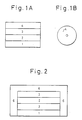
- the substrate 1 (Fig. 2) was fixed in the vacuum chamber of a radio frequency magnetron sputtering device with three targets (SPF-430 type produced by Anerva Co., Ltd.).
- the vacuum chamber was evacuated to a pressure of 4 x 10 ⁇ 7 Torr or less.
- the substrate 1 was rotated at 15 rpm and water-cooled while the sputtering was carried out.
- the gaseous mixture of Ar and O2 (10 vol%) was admitted into the vacuum chamber and the flow rate thereof was adjusted to provide a pressure of 1 x 10 ⁇ 2 Torr.
- the target of the magnetron sputtering device for the indium oxide deposition was an In2O3 sintered body having a diameter of 100 mm and a thickness of 5 mm.
- the high frequency reactive sputtering was carried out at a discharge power of 100 W and a discharge frequency of 13.56 MHz.
- an In2O3 film was deposited as the dielectric layer 2 to a thickness of approximately 800 ⁇ .
- the target to be sputtered was replaced with the target for depositing the first protecting layer 5, i.e., the Ti layer, and then the Ar gas (5N) was admitted into the vacuum chamber.
- the Ti film 5 was deposited under the same discharge conditions as above, to a thickness of approximately 10 ⁇ .
- the target to be sputtered was then replaced with the target for depositing the recording layer, i.e., Fe69Tb23Co8 alloy target, and then the argon gas (5N) was admitted into the vacuum chamber.
- the FeTbCo alloy film was deposited under the same discharge conditions as above, to a thickness of approximately 1000 ⁇ .
- the substrate having a diameter of 200 mm was masked so that the above respective, In2O3 film, Ti film and FeTbCo alloy film were deposited on the substrate from the center to a radius of 90 mm.
- the mask was finally removed to enable a film to be deposited on the entire surface of substrate.
- the target to be sputtered was then replaced with the Ti target for forming the second protecting layer 6.
- the Ti film was deposited under the same conditions as described above to a thickness of approximately 200 ⁇ .
- the magneto-optical (In/Sn-oxide/Ti) recording medium having a layer structure of PC/In2O3/Ti/FeTbCo/Ti was obtained.
- the second protecting layer 6 covers all of the layers, including the recording layer 3.
- a magneto-optical recording and reproducing unit (OMS-1000 Type (III) by Nakamichi) was used.
- the disc was rotated at 900 rpm, and signal of 1.024 MHz was recorded in the disc by means of a laser diode light of 5.0 mW.
- the signal was then read out by means of a laser diode light of 0.8 mW.
- the applied magnetic field was 500 ⁇ e.
- Table 1 The result is given in Table 1 as "Example 2".
- Example 2 The layer structure as described above was allowed to stand in a constant-temperature and humidity condition of 60°C and an RH of 90% for 1000 hours. Subsequently, the C/N ratio was measured. The result is given in Table 1 as "Example 2".
- the discrete film of In2O3 was prepared under the same conditions above and the electric resistance thereof was measured.
- the measurement revealed the film to be an insulating film having a surface resistance of 10 M ⁇ /sq or more and a volume resistivity of 8 x 10 ⁇ cm or more.
- a substrate in the form of a disc having a diameter of 200 mm, a thickness of 1.2 mm and having grooves at the pitch of 1.6 ⁇ m was made of polycarbonate resin (PC).
- the substrate 1 (Fig. 2) was fixed in the vacuum chamber of a radio frequency magnetron sputtering apparatus with three targets (SPF-430 type produced by ANELVA Co., Ltd.).
- the vacuum chamber was evacuated to a pressure of 4 x 10 ⁇ 7 Torr or less.
- the substrate 1 was rotated at 15 rpm and water-cooled while the sputtering was carried out.
- Ar gas (5N) was admitted into the vacuum chamber and flow rate thereof was adjusted to provide a pressure of 1 x 10 ⁇ 2 Torr.
- the target of the magnetron sputtering device for the dielectrics-deposition was a ZnS disc having a diameter of 100 mm and a thickness of 5 mm.
- the radio frequency reactive sputtering was carried out at a discharge power of 100 W and a discharge frequency of 13.56 MHz.
- a ZnS film was deposited as the dielectric layer 2, to a thickness of approximately 800 ⁇ .
- the target to be sputtered was replaced with the target for depositing the recording layer, i.e., the Fe69Tb23Co8 alloy target, and then the FeTbCo alloy film was deposited under the same discharge conditions as above, to a thickness of approximately 1000 ⁇ .
- the target to be sputtered was then replaced with the ZnS target for forming the protecting layer 4.
- the ZnS film was deposited under the same conditions as described above, to a thickness of approximately 800 ⁇ .
- Example 2 No change in the appearance occurred in Example 2, but wrinkles, presumably due to corrosion deterioration, were numerous in Comparative Example 2.
- Example 2 The procedure of Example 2 for producing a recording disc was repeated except that: the substrate temperature was raised to 100°C; the target was made of a sintered body of In2O3 (5 wt% SnO2); and the sputtering gas was pure Ar gas (5N).
- the obtained In2O3 (SnO2) film was transparent and conductive, and had a surface resistance of 500 ⁇ /sq and a volume resistivity of 4 x 10 ⁇ 3 ⁇ cm.
- the obtained disc was rotated at 900 rpm and a signal of 1.024 MHz was recorded by means of semiconductor laser light of 5 mW.
- the reproducing was then carried out by means of a laser diode light of 0.8 mW, and the resulting C/N ratio was 44 dB.
- the power of the laser light for writing was increased to 8.5 mW, and then an C/N ratio of 49 dB was obtained.
- the conductive transparent In2O3 (SnO2) film known as the ITO electrode, is disadvantageous in that it produces an energy loss of the laser when writing.
- the substrate 1 (Fig. 2) was fixed in the vacuum chamber of a radio frequency magnetron sputtering device with three targets (SPF-430 type produced by ANELVA Co., Ltd.). The vacuum chamber was evacuated to a pressure of 4 x 10 ⁇ 7 Torr or less. The substrate 1 was rotated at 15 rpm and water-cooled while the sputtering was carried out.
- the target of the magnetron sputtering device for the tin oxide deposition was a SnO2 sintered disc having a diameter of 100 mm and a thickness of 5 mm.
- a high frequency reactive sputtering was carried out at a discharge power of 50 W and a discharge frequency of 13.56 MHz.
- an SnO2 film was deposited as the dielectric layer 2, to a thickness of approximately 800 ⁇ .
- the target to be sputtered was replaced with the target for depositing the first protecting layer 5, i.e., a Ti target, and then the argon gas (5N) was admitted into the vacuum chamber.
- the Ti film was deposited under the same discharge conditions as above, to a thickness of approximately 10 ⁇ .
- the target to be sputtered was then replaced with the TbFeCo composite target, and then the Ar gas (5N) was admitted into the vacuum chamber.
- the FeTbCo alloy film was deposited under the same discharge conditions as above, to a thickness of approximately 1000 ⁇ .
- the target to be sputtered was then replaced with a Ti target for depositing the second protecting layer 6, and the Ti film was deposited under the same discharge conditions as above, to a thickness of approximately 200 ⁇ .
- the magnetooptical (In/Sn-oxide/Ti) recording medium having a layer structure of PC/SnOx/Ti/Fe TbCo/Ti was obtained.
- the second protecting layer 6 covers all of the layers, including the recording layer 3.
- a magneto-optical recording and reproducing unit OMS-1000 Type (III) by Nakamichi
- the disc was rotated at 900 rpm, and a signal of 1.024 MHz was recorded in the disc by means of a laser diode light of 7.5 mW.
- the signal was then read out by means of a laser diode light of 0.8 mW.
- the applied magnetic field was 500 Oe.
- Table 2 The result is given in Table 2 as "Example 3".
- Example 3 The layer structure as described above was allowed to stand in a constant-temperature and humidity condition of 60°C and an RH of 90% for 500 hours. Subsequently, the C/N ratio was measured. The result is given in Table 2 as "Example 3".
- the discrete film of SnO2 was prepared under the same conditions as above, and the electric resistance thereof was measured.
- the measurement revealed the film to be an insulating film having a surface resistance of 10 M ⁇ /sq or more and a volume resistivity of 8 x 10 ⁇ cm or more.
- a refractive index was measured by an ellipsometer (Mizoziri Co., Ltd.).
- the measurement revealed the film to be a high refractive film having an index of refraction of 2.0 at 830 nm wavelength.
- Table 2 C/N ratio Before Standing After Standing Example 3 51 dB 50 dB Comparative Example 3 51 dB 44 dB
- Example 3 A change in the appearance did not occur in Example 3, but wrinkles, presumably due to the corrosion deterioration, were numerous in Comparative Example 2. Higher power of laser diode than in Example 1 appears to result from a lower refractive index of the SnOx layer than In2O3 layer.
- ITO (In2O3-SnO2) film was formed on a water-cooled, glass substrate by means of a high frequency sputtering method, in which the pressure of an Ar-O2 (20 vol%) gaseous mixture in the vacuum chamber was 1 x 10 ⁇ 2 Torr and the target was made of an In-Sn (Sn 5 wt%) alloy.
- the ITO film had a surface resistance of 100 M ⁇ /sq or more and was dielectric.
- a magneto-optical layer was formed on a polycarbonate substrate 10 x 20 mm square and 1.2 mm thick by the high frequency sputtering in the argon gas atmosphere, using an Fe69Co8Tb23 alloy.
- the above two substrates treated by the high frequency sputtering were dipped in an aqueous solution of NaCl having a concentration of 0.1 mol/l, as electrodes in a opposed position.
- the current conducting between the electrodes was measured for 120 minutes.
- the current conduction was slight and the total quantity of electric charge was 1.4 x 10 ⁇ 2 Coulomb.
- ITO (In2O3-SnO2) film was formed on a water-cooled, glass substrate by means of a high frequency sputtering method, in which the pressure of Ar-gas in the vacuum chamber was 1 x 10 ⁇ 2 Torr, the target was made of a sintered In2O3-SnO2 (5% SnO2), and, the substrate temperature was 130°C.
- the ITO film had a surface resistance of 500 ⁇ /sq, and was conductive and transparent.
- the above substrate treated by the high frequency sputtering and the polycarbonate substrate treated in Example 6 were dipped in an aqueous solution of NaCl having a concentration of 0.1 mol/l, as electrodes in a opposed position.
- the current conducting between the electrodes was measured for 120 minutes. The current conduction was noticeable and the total quantity of electric charge was 1.3 Coulomb.
- Example 4 From Example 4 and the Comparative Examples, it will be apparent that a local electrochemical cell will be formed at the interface between the FeCoTb film and the conductive ITO film under an extremely humid condition.
- Example 2 The process of Example 2 was repeated except that instead of the In2O3 film the In2O3 containing SnO2 was formed by using a target consisting of a In2O3 - 7% by weight of SnO2.
- the obtained layer structure was PC/In2O3 (SnO2)/Ti/FeTbCo/Ti.
- Example 2 The same tests as in Example 2 were carried out and the same results as in Example 2 were obtained.
- Example 2 The process of Example 2 was repeated except that instead of the In2O3 film the In2O3 containing SnO2 was formed by using a target consisting of a In2O3 - 30% by weight of SnO2.
- the obtained layer structure was PC/In2O3 (SnO2)/Ti/FeTbCo/Ti.
- Example 2 The same tests as in Example 2 were carried out and the same results as in Example 2 were obtained.
- PMMA acrylic resin
- the substrate 1 was fixed in the vacuum chamber of a high frequency magnetron sputtering device with three targets (SPF-430 type produced by ANELVA Co., Ltd.).
- the vacuum chamber was evacuated to a pressure of 4 x 10 ⁇ 7 Torr or less, and the substrate 1 was rotated at 15 rpm and water-cooled while the sputtering was carried out.
- the target of the magnetron sputtering device for the indium oxide deposition was an In (indium) disc having a diameter of 100 mm and a thickness of 5 mm.
- a radio frequency reactive sputtering was carried out at a discharge power of 100 W and a discharge frequency of 13.56 MHz.
- an In2O3 film was deposited as the dielectric layer 2 having a thickness of approximately 800 ⁇ .
- the target to be sputtered was replaced with the target for depositing the recording layer, i.e., the Nd 7.5 Dy 17.5 Fe 52.5 Co 22.5 alloy target (number indicates the composition by atomic %), and argon gas (5N) was then admitted into the vacuum chamber.
- the NdDyFeCo alloy film was deposited under the same discharge conditions as above to a thickness of approximately 1000 ⁇ .
- the In2O3 film was deposited in the same way as the dielectric layer 2, to a thickness of approximately 800 ⁇ .
- the layer structure as described above was allowed to stand in a constant-temperature and humidity condition of 60°C and an RH of 90% for 200 hours. Subsequently, the circumferential part at the point A was observed by an optical microscope, and neither defects nor peeling were revealed, thus showing no change from the condition before standing.
- the discrete film of In2O3 was prepared under the same conditions as above, and the electric resistance thereof was measured.
- the measurement revealed the film to be an insulating film having surface resistance of 10 M ⁇ /sq or more and a volume resistivity of 8 x 10 ⁇ cm or more.
Claims (9)
- Magneto-optisches Aufzeichnungsmedium, welches umfaßt: ein transparentes Substrat (Träger) (1) aus Kunststoff, eine magneto-optische Aufzeichnungsschicht (3) und eine zwischen der magneto-optischen Aufzeichnungsschicht (3) und dem transparenten Substrat (1) angeordnete dielektrische Schicht (2), dadurch gekennzeichnet, daß die dielektrische Schicht (2) aus einem dielektrischen transparenten Oxidfilm besteht, welcher mindestens eines der folgenden Elemente enthält: In, Sn.
- Magneto-optisches Aufzeichnungsmedium nach Anspruch 1, welches ferner eine Schutzschicht (5) umfaßt, die aus einer metallischen Titanschicht zwischen der dielektrischen Schicht (2) und dem magneto-optischen Aufzeichnungsmedium (3) besteht.
- Magneto-optisches Aufzeichnungsmedium nach Anspruch 2, bei dem die Schutzschicht (5) eine Dicke von 5 nm (50 Å) oder weniger besitzt.
- Magneto-optisches Aufzeichnungsmedium nach einem der Ansprüche 1 bis 3, welches ferner eine Schutzschicht (4, 6) umfaßt, die die magneto-optische Aufzeichnungsschicht (3) auf der Seite bedeckt, die dem transparenten Substrat (1) gegenüberliegt.
- Magneto-optisches Aufzeichnungsmedium nach einem der Ansprüche 1 bis 4, bei dem die dielektrische Schicht (2) aus stöchiometrischem In₂O₃ besteht.
- Magneto-optisches Aufzeichnungsmedium nach einem der Ansprüche 1 bis 4, bei dem die dielektrische Schicht (2) hauptsächlich aus Indiumoxid und zusätzlich aus Zinnoxid besteht.
- Magneto-optisches Aufzeichnungsmedium nach Anspruch 6, bei dem das Indiumoxid In₂O₃ ist und bei dem das Zinnoxid SnO₂ ist.
- Magneto-optisches Aufzeichnungsmedium nach Anspruch 6 oder 7, bei dem der Gehalt des Zinnoxids 30 Gew.-% oder weniger beträgt.
- Magneto-optisches Aufzeichnungsmedium nach einem der Ansprüche 1 bis 4, bei dem die dielektrische Schicht (2) aus SnOx besteht, wobei x in folgendem Bereich liegt: 1 ≦ x ≦ 2.
Applications Claiming Priority (4)
| Application Number | Priority Date | Filing Date | Title |
|---|---|---|---|
| JP108663/86 | 1986-05-14 | ||
| JP61108663A JPS62266746A (ja) | 1986-05-14 | 1986-05-14 | 光記録媒体及びその製造方法 |
| JP308520/86 | 1986-12-26 | ||
| JP30852086 | 1986-12-26 |
Publications (3)
| Publication Number | Publication Date |
|---|---|
| EP0245833A2 EP0245833A2 (de) | 1987-11-19 |
| EP0245833A3 EP0245833A3 (en) | 1988-12-14 |
| EP0245833B1 true EP0245833B1 (de) | 1991-10-09 |
Family
ID=26448495
Family Applications (1)
| Application Number | Title | Priority Date | Filing Date |
|---|---|---|---|
| EP87106848A Expired - Lifetime EP0245833B1 (de) | 1986-05-14 | 1987-05-12 | Magneto-optischer Aufzeichnungsträger |
Country Status (3)
| Country | Link |
|---|---|
| US (1) | US5512364A (de) |
| EP (1) | EP0245833B1 (de) |
| DE (1) | DE3773531D1 (de) |
Families Citing this family (11)
| Publication number | Priority date | Publication date | Assignee | Title |
|---|---|---|---|---|
| US5192626A (en) * | 1988-12-14 | 1993-03-09 | Teijin Limited | Optical recording medium |
| JP2551994B2 (ja) * | 1989-05-15 | 1996-11-06 | シャープ株式会社 | 光磁気ディスクの製造方法 |
| EP0488854A3 (en) * | 1990-11-27 | 1992-11-25 | Shin-Etsu Chemical Co., Ltd. | Method for the preparation of a magneto-optical recording medium |
| AU1904100A (en) * | 1999-12-17 | 2001-06-25 | Institute Of Materials Research And Engineering | Improved transparent electrode material for quality enhancement of oled devices |
| US20050146993A1 (en) * | 2002-10-25 | 2005-07-07 | Fujitsu Limited | Magneto-optical recording medium, information recording/reproducing method, and magnetic recording apparatus |
| US7439007B2 (en) * | 2002-12-20 | 2008-10-21 | Ricoh Company, Ltd. | Phase change information recording medium having multiple layers and recording and playback method for the medium |
| US7864656B2 (en) * | 2007-05-09 | 2011-01-04 | Victor Company Of Japan, Ltd. | Optical storage medium and method of producing optical storage medium |
| JP2009080871A (ja) * | 2007-09-25 | 2009-04-16 | Taiyo Yuden Co Ltd | 光情報記録媒体 |
| FR2963342B1 (fr) * | 2010-07-27 | 2012-08-03 | Saint Gobain | Procede d'obtention d'un materiau comprenant un substrat muni d'un revetement |
| US8929698B2 (en) * | 2011-09-13 | 2015-01-06 | Seagate Technology Llc | Plasmonic transducer with reduced cross section at media-reading surface |
| US8958668B2 (en) | 2011-09-13 | 2015-02-17 | Seagate Technology Llc | Plasmonic transducer having two metal elements with a gap disposed therebetween |
Family Cites Families (23)
| Publication number | Priority date | Publication date | Assignee | Title |
|---|---|---|---|---|
| JPS5231703A (en) * | 1975-09-05 | 1977-03-10 | Kokusai Denshin Denwa Co Ltd <Kdd> | Magnetic thin film recording medium |
| JPS5922311B2 (ja) * | 1976-09-13 | 1984-05-25 | 富士写真フイルム株式会社 | 磁気記録体用リ−ダ−、トレ−ラ−テ−プ |
| JPS6032331B2 (ja) * | 1980-03-12 | 1985-07-27 | ケイディディ株式会社 | 磁気光学記録媒体 |
| US4461807A (en) * | 1980-07-25 | 1984-07-24 | Asahi Kasei Kogyo Kabushiki Kaisha | Recording material |
| EP0056852B1 (de) * | 1981-01-26 | 1985-08-28 | LGZ LANDIS & GYR ZUG AG | Ladungszelle |
| US4449138A (en) * | 1981-04-15 | 1984-05-15 | Tokyo Shibaura Denki Kabushiki Kaisha | Information recording medium |
| JPS5873746A (ja) * | 1981-10-27 | 1983-05-04 | Kokusai Denshin Denwa Co Ltd <Kdd> | 光磁気記録媒体 |
| JPS58215744A (ja) * | 1982-06-08 | 1983-12-15 | Yoshifumi Sakurai | 光熱磁気記録媒体 |
| JPS5910052A (ja) * | 1982-07-08 | 1984-01-19 | Nissin Electric Co Ltd | ル−プ式情報伝送方法 |
| JPS5979426A (ja) * | 1982-10-29 | 1984-05-08 | Tdk Corp | 磁気記録媒体 |
| DE3382791T2 (de) * | 1982-12-15 | 1995-12-07 | Sharp Kk | Magneto-optischer Speicher. |
| JPS6165846A (ja) * | 1984-09-10 | 1986-04-04 | Teijin Ltd | α,β−不飽和カルボン酸類、それを活性成分とした除草剤及び植物生長調整剤 |
| JPS60197966A (ja) * | 1984-03-22 | 1985-10-07 | Canon Inc | 光学的記録媒体 |
| JPS60197965A (ja) * | 1984-03-21 | 1985-10-07 | Canon Inc | 磁気記録媒体 |
| JPS60243844A (ja) * | 1984-05-18 | 1985-12-03 | Fujitsu Ltd | 光磁気記録媒体 |
| JPS60243842A (ja) * | 1984-05-18 | 1985-12-03 | Fujitsu Ltd | 光磁気デイスク媒体 |
| US4680742A (en) * | 1984-07-07 | 1987-07-14 | Kyocera Corporation | Magneto-optical recording element |
| JPS6129437A (ja) * | 1984-07-20 | 1986-02-10 | Canon Inc | 光磁気記録媒体 |
| JPS6150236A (ja) * | 1984-08-18 | 1986-03-12 | Canon Inc | 磁気記録媒体の製造方法 |
| JPS6157052A (ja) * | 1984-08-28 | 1986-03-22 | Canon Inc | 光学的記録媒体 |
| JPS61122955A (ja) * | 1984-11-19 | 1986-06-10 | Fujitsu Ltd | 光磁気記録媒体 |
| JPS6289255A (ja) * | 1985-10-15 | 1987-04-23 | Konishiroku Photo Ind Co Ltd | 光磁気記録媒体 |
| JPH07107750B2 (ja) * | 1986-02-21 | 1995-11-15 | コニカ株式会社 | 情報記録媒体 |
-
1987
- 1987-05-12 EP EP87106848A patent/EP0245833B1/de not_active Expired - Lifetime
- 1987-05-12 DE DE8787106848T patent/DE3773531D1/de not_active Expired - Lifetime
-
1994
- 1994-02-28 US US08/203,708 patent/US5512364A/en not_active Expired - Fee Related
Also Published As
| Publication number | Publication date |
|---|---|
| DE3773531D1 (de) | 1991-11-14 |
| US5512364A (en) | 1996-04-30 |
| EP0245833A3 (en) | 1988-12-14 |
| EP0245833A2 (de) | 1987-11-19 |
Similar Documents
| Publication | Publication Date | Title |
|---|---|---|
| EP0406569B1 (de) | Optisches Aufzeichnungsmedium | |
| EP0245833B1 (de) | Magneto-optischer Aufzeichnungsträger | |
| JPH0325737A (ja) | 光磁気記録媒体 | |
| JPH0775085B2 (ja) | 光磁気媒体 | |
| US5576102A (en) | Magneto optical recording medium | |
| JPS61144744A (ja) | 光磁気記録素子及びその製法 | |
| JP2541677B2 (ja) | 光記録媒体 | |
| JP2550118B2 (ja) | 光磁気記録媒体 | |
| EP0388852B1 (de) | Magnetooptischer Aufzeichnungsträger und Verfahren zu seiner Herstellung | |
| JP2528188B2 (ja) | 光記録媒体 | |
| JP2507592B2 (ja) | 光記録媒体 | |
| JP2523180B2 (ja) | 光記録媒体及びその製造方法 | |
| JP2528173B2 (ja) | 光記録媒体 | |
| JP2804165B2 (ja) | 光磁気記録媒体 | |
| JPH03122845A (ja) | 光記録媒体 | |
| JP2564387B2 (ja) | 積層体 | |
| KR930003871B1 (ko) | 광디스크 및 그 제조방법 | |
| JP2729664B2 (ja) | 光磁気記録媒体 | |
| JPH04263143A (ja) | 光磁気記録媒体 | |
| JP2559871B2 (ja) | 光記録媒体 | |
| JPS63167450A (ja) | 光磁気記録媒体の製造方法 | |
| EP0316803A2 (de) | Magneto-optisches Speichermedium | |
| JPS61172236A (ja) | 光磁気記録素子 | |
| JPH03142728A (ja) | 光記録媒体 | |
| JPH01245447A (ja) | 光磁気記録媒体 |
Legal Events
| Date | Code | Title | Description |
|---|---|---|---|
| PUAI | Public reference made under article 153(3) epc to a published international application that has entered the european phase |
Free format text: ORIGINAL CODE: 0009012 |
|
| AK | Designated contracting states |
Kind code of ref document: A2 Designated state(s): DE FR GB NL |
|
| PUAL | Search report despatched |
Free format text: ORIGINAL CODE: 0009013 |
|
| AK | Designated contracting states |
Kind code of ref document: A3 Designated state(s): DE FR GB NL |
|
| 17P | Request for examination filed |
Effective date: 19890311 |
|
| 17Q | First examination report despatched |
Effective date: 19901221 |
|
| GRAA | (expected) grant |
Free format text: ORIGINAL CODE: 0009210 |
|
| AK | Designated contracting states |
Kind code of ref document: B1 Designated state(s): DE FR GB NL |
|
| REF | Corresponds to: |
Ref document number: 3773531 Country of ref document: DE Date of ref document: 19911114 |
|
| ET | Fr: translation filed | ||
| PLBE | No opposition filed within time limit |
Free format text: ORIGINAL CODE: 0009261 |
|
| STAA | Information on the status of an ep patent application or granted ep patent |
Free format text: STATUS: NO OPPOSITION FILED WITHIN TIME LIMIT |
|
| 26N | No opposition filed | ||
| PGFP | Annual fee paid to national office [announced via postgrant information from national office to epo] |
Ref country code: NL Payment date: 19940531 Year of fee payment: 8 |
|
| PG25 | Lapsed in a contracting state [announced via postgrant information from national office to epo] |
Ref country code: NL Effective date: 19951201 |
|
| NLV4 | Nl: lapsed or anulled due to non-payment of the annual fee |
Effective date: 19951201 |
|
| PGFP | Annual fee paid to national office [announced via postgrant information from national office to epo] |
Ref country code: FR Payment date: 20000425 Year of fee payment: 14 |
|
| PGFP | Annual fee paid to national office [announced via postgrant information from national office to epo] |
Ref country code: GB Payment date: 20000502 Year of fee payment: 14 |
|
| PGFP | Annual fee paid to national office [announced via postgrant information from national office to epo] |
Ref country code: DE Payment date: 20000630 Year of fee payment: 14 |
|
| PG25 | Lapsed in a contracting state [announced via postgrant information from national office to epo] |
Ref country code: GB Free format text: LAPSE BECAUSE OF NON-PAYMENT OF DUE FEES Effective date: 20010512 |
|
| GBPC | Gb: european patent ceased through non-payment of renewal fee |
Effective date: 20010512 |
|
| PG25 | Lapsed in a contracting state [announced via postgrant information from national office to epo] |
Ref country code: FR Free format text: LAPSE BECAUSE OF NON-PAYMENT OF DUE FEES Effective date: 20020131 |
|
| PG25 | Lapsed in a contracting state [announced via postgrant information from national office to epo] |
Ref country code: DE Free format text: LAPSE BECAUSE OF NON-PAYMENT OF DUE FEES Effective date: 20020301 |