EP0240769B1 - Steuerscheibe für Bildwiedergabevorrichtungen - Google Patents
Steuerscheibe für Bildwiedergabevorrichtungen Download PDFInfo
- Publication number
- EP0240769B1 EP0240769B1 EP87103665A EP87103665A EP0240769B1 EP 0240769 B1 EP0240769 B1 EP 0240769B1 EP 87103665 A EP87103665 A EP 87103665A EP 87103665 A EP87103665 A EP 87103665A EP 0240769 B1 EP0240769 B1 EP 0240769B1
- Authority
- EP
- European Patent Office
- Prior art keywords
- conductors
- openings
- panel according
- controller panel
- glass frit
- Prior art date
- Legal status (The legal status is an assumption and is not a legal conclusion. Google has not performed a legal analysis and makes no representation as to the accuracy of the status listed.)
- Expired - Lifetime
Links
- 239000004020 conductor Substances 0.000 claims description 40
- 239000011521 glass Substances 0.000 claims description 24
- 229910052751 metal Inorganic materials 0.000 claims description 10
- 239000002184 metal Substances 0.000 claims description 10
- PXHVJJICTQNCMI-UHFFFAOYSA-N Nickel Chemical compound [Ni] PXHVJJICTQNCMI-UHFFFAOYSA-N 0.000 claims description 4
- VYZAMTAEIAYCRO-UHFFFAOYSA-N Chromium Chemical compound [Cr] VYZAMTAEIAYCRO-UHFFFAOYSA-N 0.000 claims description 2
- RYGMFSIKBFXOCR-UHFFFAOYSA-N Copper Chemical compound [Cu] RYGMFSIKBFXOCR-UHFFFAOYSA-N 0.000 claims description 2
- 229910052782 aluminium Inorganic materials 0.000 claims description 2
- XAGFODPZIPBFFR-UHFFFAOYSA-N aluminium Chemical compound [Al] XAGFODPZIPBFFR-UHFFFAOYSA-N 0.000 claims description 2
- 229910052802 copper Inorganic materials 0.000 claims description 2
- 239000010949 copper Substances 0.000 claims description 2
- 229910052759 nickel Inorganic materials 0.000 claims description 2
- 238000000576 coating method Methods 0.000 claims 2
- 239000002245 particle Substances 0.000 claims 2
- 239000007767 bonding agent Substances 0.000 claims 1
- 229910052804 chromium Inorganic materials 0.000 claims 1
- 239000011651 chromium Substances 0.000 claims 1
- 239000007787 solid Substances 0.000 claims 1
- 238000009825 accumulation Methods 0.000 description 6
- 230000035508 accumulation Effects 0.000 description 6
- 230000000694 effects Effects 0.000 description 2
- 239000002318 adhesion promoter Substances 0.000 description 1
- QXJJQWWVWRCVQT-UHFFFAOYSA-K calcium;sodium;phosphate Chemical compound [Na+].[Ca+2].[O-]P([O-])([O-])=O QXJJQWWVWRCVQT-UHFFFAOYSA-K 0.000 description 1
- 230000001419 dependent effect Effects 0.000 description 1
- 238000004519 manufacturing process Methods 0.000 description 1
- 238000007650 screen-printing Methods 0.000 description 1
Images

Classifications
-
- H—ELECTRICITY
- H01—ELECTRIC ELEMENTS
- H01J—ELECTRIC DISCHARGE TUBES OR DISCHARGE LAMPS
- H01J17/00—Gas-filled discharge tubes with solid cathode
- H01J17/38—Cold-cathode tubes
- H01J17/48—Cold-cathode tubes with more than one cathode or anode, e.g. sequence-discharge tube, counting tube, dekatron
- H01J17/49—Display panels, e.g. with crossed electrodes, e.g. making use of direct current
- H01J17/492—Display panels, e.g. with crossed electrodes, e.g. making use of direct current with crossed electrodes
-
- H—ELECTRICITY
- H01—ELECTRIC ELEMENTS
- H01J—ELECTRIC DISCHARGE TUBES OR DISCHARGE LAMPS
- H01J17/00—Gas-filled discharge tubes with solid cathode
- H01J17/02—Details
- H01J17/04—Electrodes; Screens
- H01J17/12—Control electrodes
-
- H—ELECTRICITY
- H01—ELECTRIC ELEMENTS
- H01J—ELECTRIC DISCHARGE TUBES OR DISCHARGE LAMPS
- H01J2217/00—Gas-filled discharge tubes
- H01J2217/38—Cold-cathode tubes
- H01J2217/49—Display panels, e.g. not making use of alternating current
- H01J2217/492—Details
- H01J2217/49264—Vessels
- H01J2217/49271—Spacers between front and back panels
Definitions
- the invention relates to a control disk for a flat image display device according to the preamble of claim 1.
- a flat image display device is known from the essay "Design, Fabrication, and Performance of a flat Tube Display” by WC Holton et al (1977 International Electron Devices Meeting, pages 78 to 80, Washington, DC, USA; IEEE) Has control stack.
- the control stack is arranged between a cathode and a fluorescent screen and is used to control the electron current. It consists of control disks, which are formed from layers of intersecting metallic conductors, between which a metal perforated disk is arranged. At the crossing points of the conductors, there are elliptical holes in the conductors which are aligned with the holes in the perforated disc.
- the ladder and the perforated disc are each connected by glass frit and kept at a certain distance.
- the invention is therefore based on the object of specifying a control disk without a disruptive influence on the electron current.
- the openings Due to the special shape of the openings, the scattering of the electrons is largely prevented and focusing is achieved, which increases the transparency of the control disk for the electrons. It is advantageous if the openings each cut the adjacent conductors, because then the glass frit between the conductors is very far away from the openings and their charging cannot have any effect.
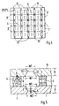
- control disks shown in the figures are provided for a flat image display device and are used to control the electron current between the cathode and the luminescent screen.
- Openings 2 are provided at regular intervals, each of which is arranged in such a way that it cuts adjacent conductors 1.
- the parting line 3 between the conductors 1 runs through the middle of the openings 2.
- the openings 2 have a rectangular shape, the long sides of which are transverse to the parting lines 3.
- FIG. 2 shows a second layer of conductors 11 which run parallel to one another.
- openings 22 at regular intervals, which are also arranged in such a way that they cut adjacent conductors 11. This means that the separating joints 33 run through the middle of the openings 22.
- the openings 22 also have a rectangular shape, the short sides of which lie transversely to the separating joints 33, and have the same dimensions as the openings 2.
- the finished control disk shown in FIG. 3 consists of the first layer of conductor 1 and the second layer of conductor 11 rotated by 90 degrees with respect to it, and accumulations of glass frit 4 arranged therebetween Glass frit 4 keeps the two layers at a certain distance from one another and connects them to one another at the same time. There may also be a glass frit edge seal between the layers (not shown).
- the clusters of glass frit 4 are each arranged at the intersection of the conductor 1 with the conductors 11. This results in the greatest possible removal of the glass frit from the openings 2 and 22. The influence of a possible charging of the glass frit is thereby limited to the smallest possible extent.
- the finished control disk shown in FIG. 4 consists of a first layer of conductors 1 ⁇ and the second layer of conductors 11 rotated by 90 degrees thereto and accumulations of glass frit 4 arranged between them.
- the openings 2 ⁇ are in the middle of the conductors 1 ⁇ , so that the joints 3 ⁇ do not run through them.
- the clusters of the glass frit 4 are closer to the openings 2 ⁇ and 22, but a simpler control circuit can be used in this embodiment.
- the control disc can be manufactured as follows: The holes 2 are etched into a first metal disk and the later joints 3 are half-etched. The holes 22 are etched into a second metal disk and the later parting lines 33 are half-etched. The glass frit 4 is applied to the first metal disc, for example by screen printing, on the surfaces provided for the accumulations. Then the second metal disc Aligned by 90 degrees, placed on the first metal disc with the glass frit and both joined together. The joints 3 and 33 are then etched through.
- Fig. 5 the section along the line V-V in Fig. 3 is shown by the control disc to show the special shape of the openings 2 and 22 and the accumulations of the glass frit 4.
- Each opening 2 or 22 narrows from both sides of the respective conductor 1 or 11 to a resultant narrowest cross-sectional line 5 or 55.
- the walls of the narrowing openings 2, 22 can form flat or curved surfaces.
- the line 5 or 55 is approximately 0 to 30% of the conductor thickness D, preferably 25% of the conductor thickness D.
- the width W1 of the opening 2 or 22 is further from that of the line 5 or 55 lying side of the conductor 1 or 11 slightly larger than the width W2 of the opening on the other side of the conductor.
- the two layers of intersecting conductors 1 and 11 are now superimposed in such a way that the widths W1 of the openings 2 and 22 point towards one another. This results in an oval shape for the cross section of the space enclosed by the openings.
- This shape largely prevents the scattering of the electrons and creates a focus of the electron current.
- the conductors 1 and 11 are held at a certain distance A from one another by accumulations of glass frit 4.
- the glass frit 4 insulating bodies for example glass spheres 6, are mixed (left side in FIG. 5).
- the bodies or glass balls 6 must have the same coefficient of expansion as the glass frit 4. Their diameter is approximately 50 to 100 ⁇ m.
- the distance A can also be achieved by applying metal 7, for example aluminum or chrome, to the conductor on the surfaces provided for the accumulation of the glass frit 4 (right side of FIG. 5) and then fritting the metal disks with the aid the glass frit 4 takes place.
- An adhesion promoter made of copper or nickel can be present between the metal 7 and the conductors 1, 11 (not shown).
Landscapes
- Cathode-Ray Tubes And Fluorescent Screens For Display (AREA)
Applications Claiming Priority (2)
| Application Number | Priority Date | Filing Date | Title |
|---|---|---|---|
| DE3609967 | 1986-03-25 | ||
| DE19863609967 DE3609967A1 (de) | 1986-03-25 | 1986-03-25 | Steuerscheibe fuer bildwiedergabevorrichtungen |
Publications (3)
| Publication Number | Publication Date |
|---|---|
| EP0240769A2 EP0240769A2 (de) | 1987-10-14 |
| EP0240769A3 EP0240769A3 (en) | 1990-02-14 |
| EP0240769B1 true EP0240769B1 (de) | 1992-10-07 |
Family
ID=6297188
Family Applications (1)
| Application Number | Title | Priority Date | Filing Date |
|---|---|---|---|
| EP87103665A Expired - Lifetime EP0240769B1 (de) | 1986-03-25 | 1987-03-13 | Steuerscheibe für Bildwiedergabevorrichtungen |
Country Status (5)
| Country | Link |
|---|---|
| US (1) | US4745332A (enExample) |
| EP (1) | EP0240769B1 (enExample) |
| JP (1) | JPS62232839A (enExample) |
| CA (1) | CA1273987A (enExample) |
| DE (2) | DE3609967A1 (enExample) |
Families Citing this family (9)
| Publication number | Priority date | Publication date | Assignee | Title |
|---|---|---|---|---|
| DE3708798A1 (de) * | 1987-03-18 | 1988-09-29 | Standard Elektrik Lorenz Ag | Steuerscheibe fuer bildwiedergabevorrichtungen |
| US5256937A (en) * | 1989-04-07 | 1993-10-26 | Nokia (Deutschland) Gmbh | Flat panel fluorescent screen display tube |
| DE3911355A1 (de) * | 1989-04-07 | 1990-10-11 | Nokia Unterhaltungselektronik | Steueranordnung fuer eine flache anzeigeeinrichtung |
| JPH0322328A (ja) * | 1989-06-19 | 1991-01-30 | Matsushita Electric Ind Co Ltd | 平板型画像表示装置 |
| JPH0662499U (ja) * | 1993-02-10 | 1994-09-02 | 富士電子工業株式会社 | 高周波加熱コイル |
| US5600203A (en) * | 1993-04-26 | 1997-02-04 | Futaba Denshi Kogyo Kabushiki Kaisha | Airtight envelope for image display panel, image display panel and method for producing same |
| US5789857A (en) * | 1994-11-22 | 1998-08-04 | Futaba Denshi Kogyo K.K. | Flat display panel having spacers |
| JP2727995B2 (ja) * | 1994-12-15 | 1998-03-18 | 双葉電子工業株式会社 | 支柱材整列用治具および支柱材整列用治具の製造方法 |
| US5898266A (en) | 1996-07-18 | 1999-04-27 | Candescent Technologies Corporation | Method for displaying frame of pixel information on flat panel display |
Family Cites Families (7)
| Publication number | Priority date | Publication date | Assignee | Title |
|---|---|---|---|---|
| DE2844512C2 (de) * | 1978-10-12 | 1980-11-20 | Siemens Ag | Steuerplatte zur Matrixansteuerung einzelner Bildpunkte nach Zeile und Spalte auf einem Bildschirm in flachen Plasmabildwiedergabevorrichtungen |
| EP0024656B1 (en) * | 1979-08-16 | 1984-03-21 | Kabushiki Kaisha Toshiba | Flat display device |
| FR2549288B1 (fr) * | 1983-07-11 | 1985-10-25 | Hyperelec | Element multiplicateur d'electrons, dispositif multiplicateur d'electrons comportant cet element multiplicateur et application a un tube photomultiplicateur |
| JPS6023933A (ja) * | 1983-07-20 | 1985-02-06 | Toshiba Corp | マスク集束型カラ−受像管 |
| JPS6025142A (ja) * | 1983-07-21 | 1985-02-07 | Matsushita Electric Ind Co Ltd | 表示装置の電極製造方法 |
| DE3335598A1 (de) * | 1983-09-30 | 1985-04-18 | Siemens AG, 1000 Berlin und 8000 München | Verfahren zur herstellung einer elektrodenplatte, danach hergestellte elektrodenplatte und ihre verwendung |
| DE3429082A1 (de) * | 1984-08-07 | 1986-02-27 | Siemens AG, 1000 Berlin und 8000 München | Steuerscheibe fuer gasentladungsanzeige |
-
1986
- 1986-03-25 DE DE19863609967 patent/DE3609967A1/de not_active Withdrawn
-
1987
- 1987-03-11 JP JP62054299A patent/JPS62232839A/ja active Granted
- 1987-03-12 US US07/025,225 patent/US4745332A/en not_active Expired - Fee Related
- 1987-03-13 EP EP87103665A patent/EP0240769B1/de not_active Expired - Lifetime
- 1987-03-13 DE DE8787103665T patent/DE3782078D1/de not_active Expired - Lifetime
- 1987-03-24 CA CA000532852A patent/CA1273987A/en not_active Expired - Lifetime
Also Published As
| Publication number | Publication date |
|---|---|
| DE3609967A1 (de) | 1987-10-01 |
| JPS62232839A (ja) | 1987-10-13 |
| EP0240769A2 (de) | 1987-10-14 |
| EP0240769A3 (en) | 1990-02-14 |
| JPH056789B2 (enExample) | 1993-01-27 |
| CA1273987A (en) | 1990-09-11 |
| US4745332A (en) | 1988-05-17 |
| DE3782078D1 (de) | 1992-11-12 |
Similar Documents
| Publication | Publication Date | Title |
|---|---|---|
| EP1061783B2 (de) | Keramik-Metall-Substrat, insbesondere Mehrfachsubstrat | |
| DE2813968C2 (de) | Halbleiteranordnung | |
| DE3319311C2 (de) | Verfahren zur Herstellung eines elektroakustischen Wandlers mit feststehender Elektrode und dieser gegenüberstehender Membran | |
| DE69909663T2 (de) | Elektronisches Vielschichtbauteil und Verfahren zu seiner Herstellung | |
| DE4319944A1 (de) | Mehrfach-Substrat sowie Verfahren zu seiner Herstellung | |
| DE2119040A1 (de) | Mehrschichtiger Kondensator und Verfahren zur Einstellung des Kapazi tatswertes | |
| EP0655275A1 (de) | Statische Mischvorrichtung | |
| DE69838727T2 (de) | Ptc thermistorchip sowie seine herstellungsmethode | |
| DE68910015T2 (de) | Struktur mit detailliertem Muster und Herstellungsverfahren. | |
| EP0240769B1 (de) | Steuerscheibe für Bildwiedergabevorrichtungen | |
| DE19739494C2 (de) | Piezoelektrisches Element und Verfahren zur Herstellung desselben | |
| DE102011080468B4 (de) | Verfahren zur Herstellung eines Kontaktträgers eines Schaltkontaktes für ein elektromechanisches Schaltgerät sowie ein solcher Kontaktträger | |
| DE68915885T2 (de) | Verbindungsvorrichtung zwischen einer integrierten Schaltung und einer elektrischen Schaltung und Herstellungsverfahren derselben. | |
| DE4328474C2 (de) | Mehrschichtverbindungsstruktur für eine Halbleitereinrichtung | |
| DE69524571T2 (de) | Gerät mit dielektrischem resonator im zweifach-tm-modus mit fenster zur kopplung elektromagnetischer felder und bandpassfiltergerät damit | |
| DE3032486C2 (de) | Elektronenstrahlsystem für Fernsehbildröhren | |
| EP0041679A2 (de) | Verfahren zur Herstellung von elektrischen Bauelementen, insbesondere Schichtkondensatoren | |
| DE3011011C2 (de) | Plattenwärmetauscher mit in einem Stapel angeordneten rechteckigen Platten | |
| WO2002027740A1 (de) | Bewegbarer kontaktträger für einen niederspannungs-leistungsschalter mit einem abstandhalter für die kontakthebel | |
| DE9217155U1 (de) | Schaltungsanordnung | |
| DE2611871A1 (de) | Elektrische schaltungsbaugruppe in mehrschichtbauweise und verfahren zu deren herstellung | |
| DE60130969T2 (de) | Integriertes Mikrowellenmodul und entsprechendes Verfahren zu dessen Herstellung | |
| DE3023853A1 (de) | Vorbeschichtete widerstandsbehaftete linsenstruktur fuer ein elektronenstrahlsystem und verfahren zu dessen herstellung | |
| DE9310299U1 (de) | Mehrfach-Substrat | |
| DE3013773C2 (de) | Elektrischer Schreibkopf |
Legal Events
| Date | Code | Title | Description |
|---|---|---|---|
| PUAI | Public reference made under article 153(3) epc to a published international application that has entered the european phase |
Free format text: ORIGINAL CODE: 0009012 |
|
| AK | Designated contracting states |
Kind code of ref document: A2 Designated state(s): DE FR GB IT NL |
|
| RAP1 | Party data changed (applicant data changed or rights of an application transferred) |
Owner name: NOKIA GRAETZ GESELLSCHAFT MIT BESCHRAENKTER HAFTUN |
|
| RAP1 | Party data changed (applicant data changed or rights of an application transferred) |
Owner name: NOKIA UNTERHALTUNGSELEKTRONIK (DEUTSCHLAND) GMBH |
|
| PUAL | Search report despatched |
Free format text: ORIGINAL CODE: 0009013 |
|
| AK | Designated contracting states |
Kind code of ref document: A3 Designated state(s): DE FR GB IT NL |
|
| 17P | Request for examination filed |
Effective date: 19900319 |
|
| 17Q | First examination report despatched |
Effective date: 19920324 |
|
| RAP1 | Party data changed (applicant data changed or rights of an application transferred) |
Owner name: NOKIA (DEUTSCHLAND) GMBH |
|
| GRAA | (expected) grant |
Free format text: ORIGINAL CODE: 0009210 |
|
| AK | Designated contracting states |
Kind code of ref document: B1 Designated state(s): DE FR GB IT NL |
|
| REF | Corresponds to: |
Ref document number: 3782078 Country of ref document: DE Date of ref document: 19921112 |
|
| ITF | It: translation for a ep patent filed | ||
| GBT | Gb: translation of ep patent filed (gb section 77(6)(a)/1977) | ||
| ET | Fr: translation filed | ||
| PGFP | Annual fee paid to national office [announced via postgrant information from national office to epo] |
Ref country code: GB Payment date: 19930225 Year of fee payment: 7 |
|
| PG25 | Lapsed in a contracting state [announced via postgrant information from national office to epo] |
Ref country code: GB Effective date: 19930313 |
|
| PLBE | No opposition filed within time limit |
Free format text: ORIGINAL CODE: 0009261 |
|
| STAA | Information on the status of an ep patent application or granted ep patent |
Free format text: STATUS: NO OPPOSITION FILED WITHIN TIME LIMIT |
|
| 26N | No opposition filed | ||
| PG25 | Lapsed in a contracting state [announced via postgrant information from national office to epo] |
Ref country code: NL Effective date: 19931001 |
|
| GBPC | Gb: european patent ceased through non-payment of renewal fee |
Effective date: 19930313 |
|
| NLV4 | Nl: lapsed or anulled due to non-payment of the annual fee | ||
| PG25 | Lapsed in a contracting state [announced via postgrant information from national office to epo] |
Ref country code: FR Effective date: 19931130 |
|
| PG25 | Lapsed in a contracting state [announced via postgrant information from national office to epo] |
Ref country code: DE Effective date: 19931201 |
|
| REG | Reference to a national code |
Ref country code: FR Ref legal event code: ST |
|
| PG25 | Lapsed in a contracting state [announced via postgrant information from national office to epo] |
Ref country code: IT Free format text: LAPSE BECAUSE OF NON-PAYMENT OF DUE FEES;WARNING: LAPSES OF ITALIAN PATENTS WITH EFFECTIVE DATE BEFORE 2007 MAY HAVE OCCURRED AT ANY TIME BEFORE 2007. THE CORRECT EFFECTIVE DATE MAY BE DIFFERENT FROM THE ONE RECORDED. Effective date: 20050313 |