EP0240769B1 - Control plate for image reproduction devices - Google Patents
Control plate for image reproduction devices Download PDFInfo
- Publication number
- EP0240769B1 EP0240769B1 EP87103665A EP87103665A EP0240769B1 EP 0240769 B1 EP0240769 B1 EP 0240769B1 EP 87103665 A EP87103665 A EP 87103665A EP 87103665 A EP87103665 A EP 87103665A EP 0240769 B1 EP0240769 B1 EP 0240769B1
- Authority
- EP
- European Patent Office
- Prior art keywords
- conductors
- openings
- panel according
- controller panel
- glass frit
- Prior art date
- Legal status (The legal status is an assumption and is not a legal conclusion. Google has not performed a legal analysis and makes no representation as to the accuracy of the status listed.)
- Expired - Lifetime
Links
Images

Classifications
-
- H—ELECTRICITY
- H01—ELECTRIC ELEMENTS
- H01J—ELECTRIC DISCHARGE TUBES OR DISCHARGE LAMPS
- H01J17/00—Gas-filled discharge tubes with solid cathode
- H01J17/38—Cold-cathode tubes
- H01J17/48—Cold-cathode tubes with more than one cathode or anode, e.g. sequence-discharge tube, counting tube, dekatron
- H01J17/49—Display panels, e.g. with crossed electrodes, e.g. making use of direct current
- H01J17/492—Display panels, e.g. with crossed electrodes, e.g. making use of direct current with crossed electrodes
-
- H—ELECTRICITY
- H01—ELECTRIC ELEMENTS
- H01J—ELECTRIC DISCHARGE TUBES OR DISCHARGE LAMPS
- H01J17/00—Gas-filled discharge tubes with solid cathode
- H01J17/02—Details
- H01J17/04—Electrodes; Screens
- H01J17/12—Control electrodes
-
- H—ELECTRICITY
- H01—ELECTRIC ELEMENTS
- H01J—ELECTRIC DISCHARGE TUBES OR DISCHARGE LAMPS
- H01J2217/00—Gas-filled discharge tubes
- H01J2217/38—Cold-cathode tubes
- H01J2217/49—Display panels, e.g. not making use of alternating current
- H01J2217/492—Details
- H01J2217/49264—Vessels
- H01J2217/49271—Spacers between front and back panels
Definitions
- the invention relates to a control disk for a flat image display device according to the preamble of claim 1.
- a flat image display device is known from the essay "Design, Fabrication, and Performance of a flat Tube Display” by WC Holton et al (1977 International Electron Devices Meeting, pages 78 to 80, Washington, DC, USA; IEEE) Has control stack.
- the control stack is arranged between a cathode and a fluorescent screen and is used to control the electron current. It consists of control disks, which are formed from layers of intersecting metallic conductors, between which a metal perforated disk is arranged. At the crossing points of the conductors, there are elliptical holes in the conductors which are aligned with the holes in the perforated disc.
- the ladder and the perforated disc are each connected by glass frit and kept at a certain distance.
- the invention is therefore based on the object of specifying a control disk without a disruptive influence on the electron current.
- the openings Due to the special shape of the openings, the scattering of the electrons is largely prevented and focusing is achieved, which increases the transparency of the control disk for the electrons. It is advantageous if the openings each cut the adjacent conductors, because then the glass frit between the conductors is very far away from the openings and their charging cannot have any effect.
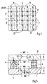
- control disks shown in the figures are provided for a flat image display device and are used to control the electron current between the cathode and the luminescent screen.
- Openings 2 are provided at regular intervals, each of which is arranged in such a way that it cuts adjacent conductors 1.
- the parting line 3 between the conductors 1 runs through the middle of the openings 2.
- the openings 2 have a rectangular shape, the long sides of which are transverse to the parting lines 3.
- FIG. 2 shows a second layer of conductors 11 which run parallel to one another.
- openings 22 at regular intervals, which are also arranged in such a way that they cut adjacent conductors 11. This means that the separating joints 33 run through the middle of the openings 22.
- the openings 22 also have a rectangular shape, the short sides of which lie transversely to the separating joints 33, and have the same dimensions as the openings 2.
- the finished control disk shown in FIG. 3 consists of the first layer of conductor 1 and the second layer of conductor 11 rotated by 90 degrees with respect to it, and accumulations of glass frit 4 arranged therebetween Glass frit 4 keeps the two layers at a certain distance from one another and connects them to one another at the same time. There may also be a glass frit edge seal between the layers (not shown).
- the clusters of glass frit 4 are each arranged at the intersection of the conductor 1 with the conductors 11. This results in the greatest possible removal of the glass frit from the openings 2 and 22. The influence of a possible charging of the glass frit is thereby limited to the smallest possible extent.
- the finished control disk shown in FIG. 4 consists of a first layer of conductors 1 ⁇ and the second layer of conductors 11 rotated by 90 degrees thereto and accumulations of glass frit 4 arranged between them.
- the openings 2 ⁇ are in the middle of the conductors 1 ⁇ , so that the joints 3 ⁇ do not run through them.
- the clusters of the glass frit 4 are closer to the openings 2 ⁇ and 22, but a simpler control circuit can be used in this embodiment.
- the control disc can be manufactured as follows: The holes 2 are etched into a first metal disk and the later joints 3 are half-etched. The holes 22 are etched into a second metal disk and the later parting lines 33 are half-etched. The glass frit 4 is applied to the first metal disc, for example by screen printing, on the surfaces provided for the accumulations. Then the second metal disc Aligned by 90 degrees, placed on the first metal disc with the glass frit and both joined together. The joints 3 and 33 are then etched through.
- Fig. 5 the section along the line V-V in Fig. 3 is shown by the control disc to show the special shape of the openings 2 and 22 and the accumulations of the glass frit 4.
- Each opening 2 or 22 narrows from both sides of the respective conductor 1 or 11 to a resultant narrowest cross-sectional line 5 or 55.
- the walls of the narrowing openings 2, 22 can form flat or curved surfaces.
- the line 5 or 55 is approximately 0 to 30% of the conductor thickness D, preferably 25% of the conductor thickness D.
- the width W1 of the opening 2 or 22 is further from that of the line 5 or 55 lying side of the conductor 1 or 11 slightly larger than the width W2 of the opening on the other side of the conductor.
- the two layers of intersecting conductors 1 and 11 are now superimposed in such a way that the widths W1 of the openings 2 and 22 point towards one another. This results in an oval shape for the cross section of the space enclosed by the openings.
- This shape largely prevents the scattering of the electrons and creates a focus of the electron current.
- the conductors 1 and 11 are held at a certain distance A from one another by accumulations of glass frit 4.
- the glass frit 4 insulating bodies for example glass spheres 6, are mixed (left side in FIG. 5).
- the bodies or glass balls 6 must have the same coefficient of expansion as the glass frit 4. Their diameter is approximately 50 to 100 ⁇ m.
- the distance A can also be achieved by applying metal 7, for example aluminum or chrome, to the conductor on the surfaces provided for the accumulation of the glass frit 4 (right side of FIG. 5) and then fritting the metal disks with the aid the glass frit 4 takes place.
- An adhesion promoter made of copper or nickel can be present between the metal 7 and the conductors 1, 11 (not shown).
Description
Die Erfindung bezieht sich auf eine Steuerscheibe für eine flache Bildwiedergabevorrichtung gemäß dem Oberbegriff des Anspruchs 1.The invention relates to a control disk for a flat image display device according to the preamble of
Aus dem Aufsatz "Design, Fabrication, and Performance of a flat Tube Display" von W.C. Holton et al (1977 International Electron Devices Meeting, Seiten 78 bis 80, Washington, DC, USA; IEEE) ist eine flache Bildwiedergabevorrichtung bekannt, die einen vielschichtigen Steuerstapel aufweist. Der Steuerstapel ist zwischen einer Kathode und einem Leuchtschirm angeordnet und dient zur Steuerung des Elektronenstromes. Er besteht aus Steuerscheiben, die aus Lagen sich kreuzender metallischer Leiter, zwischen denen eine metallene Lochscheibe angeordnet ist, gebildet sind. An den Kreuzungspunkten der Leiter sind elliptische Löcher in den Leitern vorhanden, die mit den Löchern in der Lochscheibe fluchten. Die Leiter und die Lochscheibe sind jeweils durch Glasfritte miteinander verbunden und in einem bestimmten Abstand gehalten. Mehrere solcher Steuerscheiben sind zu dem Steuerstapel zusammengebaut.A flat image display device is known from the essay "Design, Fabrication, and Performance of a flat Tube Display" by WC Holton et al (1977 International Electron Devices Meeting, pages 78 to 80, Washington, DC, USA; IEEE) Has control stack. The control stack is arranged between a cathode and a fluorescent screen and is used to control the electron current. It consists of control disks, which are formed from layers of intersecting metallic conductors, between which a metal perforated disk is arranged. At the crossing points of the conductors, there are elliptical holes in the conductors which are aligned with the holes in the perforated disc. The ladder and the perforated disc are each connected by glass frit and kept at a certain distance. Several such control disks are assembled into the control stack.
Um eine gleichmäßige Steuerung des Elektronenstromes zu erreichen, müssen Streuungen von Elektronen in den Löchern vermieden werden und die Aufladungen der isolierenden Teile der Steuerscheibe dürfen keine störenden Auswirkungen haben. Der Erfindung liegt daher die Aufgabe zugrunde, eine Steuerscheibe ohne störenden Einfluß auf den Elektronenstrom anzugeben.In order to achieve a uniform control of the electron current, scattering of electrons in the holes must be avoided and the charges on the insulating parts of the control disk must not have any disruptive effects. The invention is therefore based on the object of specifying a control disk without a disruptive influence on the electron current.
Die Lösung dieser Aufgabe erfolgt mit den im Anspruch 1 angegebenen Mitteln. Vorteilhafte Ausgestaltungen der Erfindung sind in den abhängigen Ansprüchen 2 bis 10 enthalten..This object is achieved with the means specified in
Durch die besondere Form der Öffnungen wird die Streuung der Elektronen weitgehend unterbunden und eine Fokussierung erreicht, wodurch die Transparenz der Steuerscheibe für die Elektronen gesteigert wird. Von Vorteil ist es, wenn die Öffnungen jeweils die benachbarten Leiter anschneiden, denn dann ist die Glasfritte zwischen den Leitern sehr weit von den Öffnungen entfernt und ihre Aufladung kann sich nicht auswirken.Due to the special shape of the openings, the scattering of the electrons is largely prevented and focusing is achieved, which increases the transparency of the control disk for the electrons. It is advantageous if the openings each cut the adjacent conductors, because then the glass frit between the conductors is very far away from the openings and their charging cannot have any effect.
Die Erfindung wird nachstehend anhand von in den Figuren gezeigten Ausführungsbeispielen näher erläutert. Es zeigen:
- Fig. 1
- die Draufsicht auf die Leiter der ersten Lage;
- Fig. 2
- die Draufsicht auf die Leiter der zweiten Lage;
- Fig. 3
- die Draufsicht auf eine Steuerscheibe;
- Fig. 4
- die Draufsicht auf eine andere Ausführung der Steuerscheibe und
- Fig. 5
- den Schnitt entlang der Linie V-V in Fig. 3.
- Fig. 1
- the top view of the ladder of the first layer;
- Fig. 2
- the top view of the ladder of the second layer;
- Fig. 3
- the top view of a control disc;
- Fig. 4
- the top view of another version of the control disc and
- Fig. 5
- the section along the line VV in Fig. 3rd
Die in den Figuren gezeigten Steuerscheiben sind für eine flache Bildwiedergabevorrichtung vorgesehen und dienen zur Steuerung des Elektronenstromes zwischen der Kathode und dem Leuchtschirm.The control disks shown in the figures are provided for a flat image display device and are used to control the electron current between the cathode and the luminescent screen.
In Fig. 1 ist eine erste Lage Leiter 1 dargestellt, die zueinander parallel verlaufen. Im regelmäßigen Abstand sind Öffnungen 2 vorhanden, die jeweils so angeordnet sind, daß sie benachbarte Leiter 1 anschneiden. Mit anderen Worten gesagt, verläuft die Trennfuge 3 zwischen den Leitern 1 mitten durch die Öffnungen 2. Die Öffnungen 2 haben eine rechteckige Form, deren lange Seiten quer zu den Trennfugen 3 liegen.1 shows a first layer of
In Fig. 2 ist eine zweite Lage Leiter 11 dargestellt, die zueinander parallel verlaufen. Auch hier sind im regemäßigen Abstand Öffnungen 22 vorhanden, die ebenfalls so angeordnet sind, daß sie benachbarte Leiter 11 anschneiden. Das heißt, die Trennfugen 33 verlaufen mitten durch die Öffnungen 22. Auch die Öffnungen 22 weisen eine rechteckige Form auf, deren kurze Seiten quer zu den Trennfugen 33 liegen, und haben die gleichen Abmessungen wie die Öffnungen 2.2 shows a second layer of
Die In Fig. 3 gezeigte fertige Steuerscheibe besteht aus der ersten Lage Leiter 1 und der um 90 Grad dazu verdrehten zweiten Lage der Leiter 11 und dazwischen angebrachten Anhäufungen aus Glasfritte 4. Die Glasfritte 4 hält die beiden Lagen in einem bestimmten Abstand voneinander und verbindet sie gleichzeitig miteinander. Es kann zwischen den Lagen auch noch eine Randversiegelung aus Glasfritte vorhanden sein (nicht dargestellt).The finished control disk shown in FIG. 3 consists of the first layer of
Die Anhäufungen aus Glasfritte 4 sind jeweils im Kreuzungspunkt der Leiter 1 mit den Leitern 11 angeordnet. Daraus ergibt sich die größtmögliche Entfernung der Glasfritte von den Öffnungenn 2 und 22. Der Einfluß einer eventuellen Aufladung der Glasfritte ist dadurch auf das geringstmögliche Maß beschränkt.The clusters of glass frit 4 are each arranged at the intersection of the
Die in Fig. 4 gezeigte fertige Steuerscheibe besteht aus einer ersten Lage Leiter 1ʹ und der um 90 Grad dazu verdrehten zweiten Lage der Leiter 11 und dazwischen angebrachten Anhäufungen aus Glasfritte 4. Bei den Leitern 1ʹ befinden sich die Öffnungen 2ʹ mitten in den Leitern 1ʹ, so daß die Trennfugen 3ʹ nicht durch sie hindurch laufen. Hierdurch liegen zwar die Anhäufungen der Glasfritte 4 näher an den Öffnungen 2ʹ und 22, dafür kann bei dieser Ausführungsform eine einfachere Ansteuerschaltung verwendet werden.The finished control disk shown in FIG. 4 consists of a first layer of conductors 1ʹ and the second layer of
Die Herstellung der Steuerscheibe kann folgendermaßen erfolgen:
In eine erste Metallscheibe werden die Löcher 2 geätzt und die späteren Trennfugen 3 halbgeätzt. In eine zweite Metallscheibe werden die Löcher 22 geätzt und die späteren Trennfugen 33 halbgeätzt. Auf die erste Metallscheibe wird beispielsweise durch Siebdruck die Glasfritte 4 an den für die Anhäufungen vorgesehenen Flächen aufgebracht. Dann wird die zweite Metallscheibe um 90 Grad verdreht ausgerichtet auf die mit der Glasfritte versehene erste Metallscheibe gelegt und beide miteinander zusammengefrittet. Anschließend werden die Trennfugen 3 und 33 durchgeätzt.The control disc can be manufactured as follows:
The
Es sei angemerkt, daß auch mehrere Lagen metallischer Leiter miteinander zu einer Steuerscheibe zusammengebaut werden können.It should be noted that several layers of metallic conductors can also be assembled to form a control disk.
In Fig. 5 ist der Schnitt entlang der Linie V-V in Fig. 3 durch die Steuerscheibe dargestellt, um die besondere Ausformung der Öffnungen 2 und 22 und die Anhäufungen der Glasfritte 4 zu zeigen. Jede Öffnung 2 bzw. 22 verengt sich von beiden Seiten der jeweiligen Leiter 1 bzw. 11 aus bis zu einer sich ergebenden engsten Querschnittslinie 5 bzw. 55. Die Wände der sich verengenden Öffnungen 2, 22 können ebene oder gewölbte Flächen bilden. Die Linie 5 bzw. 55 liegt bei etwa 0 bis 30% der Leiterdicke D, vorzugsweise bei 25% der Leiterdicke D. In diesem Falle ist dann die Weite W1 der Öffnung 2 bzw. 22 auf der von der Linie 5 bzw. 55 weiter ab liegenden Seite der Leiter 1 bzw. 11 etwas größer als die Weite W2 der Öffnung auf der anderen Seite der Leiter. Die beiden Lagen sich kreuzender Leiter 1 und 11 sind nun derart aufeinandergelegt, daß die Weiten W1 der Öffnungen 2 bzw. 22 aufeinander zu zeigen. Hierdurch ergibt sich für den Querschnitt des von den Öffnungen umfaßten Raumes eine ovale Form.In Fig. 5 the section along the line V-V in Fig. 3 is shown by the control disc to show the special shape of the
Diese Form verhindert weitgehend die Streuung der Elektronen und erzeugt eine Fokussierung des Elektronenstromes.This shape largely prevents the scattering of the electrons and creates a focus of the electron current.
Die Leiter 1 und 11 werden durch Anhäufungen aus Glasfritte 4 in einem bestimmten Abstand A voneinander gehalten. Um zur Vermeidung von großen Kapazitäten zwischen den Leitern 1 und 11 einen ausreichenden Abstand A zu erhalten, sind der Glasfritte 4 isolierende Körper, beispielsweise Glaskugeln 6, bemengt (linke Seite in Fig. 5). Die Körper bzw. Glaskugeln 6 müssen den gleichen Ausdehnungskoeffizienten aufweisen wie die Glasfritte 4. Ihr Durchmesser beträgt etwa 50 bis 100 um.The
Der Abstand A kann aber auch dadurch erreicht werden, daß an den für die Anhäufungen der Glasfritte 4 vorgesehenen Flächen Metall 7, beispielsweise Aluminium oder Chrom, auf die Leiter aufgetragen wird (rechte Seite der Fig. 5) und dann das Zusammenfritten der Metallscheiben mit Hilfe der Glasfritte 4 erfolgt. Zwischen dem Metall 7 und den Leitern 1, 11 kann ein Haftvermittler aus Kupfer oder Nickel vorhanden sein (nicht dargestellt).However, the distance A can also be achieved by applying metal 7, for example aluminum or chrome, to the conductor on the surfaces provided for the accumulation of the glass frit 4 (right side of FIG. 5) and then fritting the metal disks with the aid the
Claims (10)
- Controller panel for a flat image reproduction device made of layers of intersecting metallic conductors that are provided with openings arranged in a regular pattern, are joined to one another by glass frit, and are held at a defined distance from one another,
characterized in that
the openings (2; 22) taper from the two sides of the conductors (1; 11). - Controller panel according to Claim 1, characterized in that the resulting smallest cross section is located on a line (5; 55) at 0 to 30% of the conductor thickness (D), and that the widths (W2) of the openings (2; 22) on the side of the conductors (1; 11) located closer to the line (5; 55) are smaller than the widths (W1) of the openings (2; 22) on the other side of the conductors.
- Controller panel according to Claim 2, characterized in that the line (5; 55) is located at 25% of the conductor thickness.
- Controller panel according to Claim 2 or 3, characterized in that each two layers of conductors (1; 11) are arranged so that the openings (2; 22) have their greater widths (W1) opposite one another.
- Controller panel according to Claim 1, characterized in that the openings (2; 22) in at least one layer of the metallic conductors cut into the respective adjacent conductors (1; 11), and the glass frit is present at each intersection point of the conductors (1; 11).
- Controller panel according to Claim 5, characterized in that the openings (2; 22) are rectangular.
- Controller panel according to Claim 5, characterized in that the glass frit (4) contains insulating solid particles.
- Controller panel according to Claim 7, characterized in that the particles consist of glass balls (6).
- Controller panel according to Claim 5, characterized in that the conductors (1; 11) have at their intersection points metal coatings (7) between which the glass frit (4) is present.
- Controller panel according to Claim 9, characterized in that the coatings are made of aluminum or chromium, and that a bonding agent made of copper or nickel is present between them and the conductors (1; 11).
Applications Claiming Priority (2)
| Application Number | Priority Date | Filing Date | Title |
|---|---|---|---|
| DE3609967 | 1986-03-25 | ||
| DE19863609967 DE3609967A1 (en) | 1986-03-25 | 1986-03-25 | CONTROL DISC FOR IMAGE DISPLAY DEVICES |
Publications (3)
| Publication Number | Publication Date |
|---|---|
| EP0240769A2 EP0240769A2 (en) | 1987-10-14 |
| EP0240769A3 EP0240769A3 (en) | 1990-02-14 |
| EP0240769B1 true EP0240769B1 (en) | 1992-10-07 |
Family
ID=6297188
Family Applications (1)
| Application Number | Title | Priority Date | Filing Date |
|---|---|---|---|
| EP87103665A Expired - Lifetime EP0240769B1 (en) | 1986-03-25 | 1987-03-13 | Control plate for image reproduction devices |
Country Status (5)
| Country | Link |
|---|---|
| US (1) | US4745332A (en) |
| EP (1) | EP0240769B1 (en) |
| JP (1) | JPS62232839A (en) |
| CA (1) | CA1273987A (en) |
| DE (2) | DE3609967A1 (en) |
Families Citing this family (9)
| Publication number | Priority date | Publication date | Assignee | Title |
|---|---|---|---|---|
| DE3708798A1 (en) * | 1987-03-18 | 1988-09-29 | Standard Elektrik Lorenz Ag | CONTROL DISC FOR IMAGE DISPLAY DEVICES |
| DE3911355A1 (en) * | 1989-04-07 | 1990-10-11 | Nokia Unterhaltungselektronik | Control arrangement for a flat display device |
| US5256937A (en) * | 1989-04-07 | 1993-10-26 | Nokia (Deutschland) Gmbh | Flat panel fluorescent screen display tube |
| JPH0322328A (en) * | 1989-06-19 | 1991-01-30 | Matsushita Electric Ind Co Ltd | Flat type image display device |
| JPH0662499U (en) * | 1993-02-10 | 1994-09-02 | 富士電子工業株式会社 | High frequency heating coil |
| KR0148284B1 (en) * | 1993-04-26 | 1998-11-16 | 호소야 레이지 | Airtight envelope for image display panel, image display panel and method for producing the same |
| US5789857A (en) * | 1994-11-22 | 1998-08-04 | Futaba Denshi Kogyo K.K. | Flat display panel having spacers |
| JP2727995B2 (en) * | 1994-12-15 | 1998-03-18 | 双葉電子工業株式会社 | Supporting material alignment jig and method of manufacturing support material alignment jig |
| US5898266A (en) * | 1996-07-18 | 1999-04-27 | Candescent Technologies Corporation | Method for displaying frame of pixel information on flat panel display |
Family Cites Families (7)
| Publication number | Priority date | Publication date | Assignee | Title |
|---|---|---|---|---|
| DE2844512C2 (en) * | 1978-10-12 | 1980-11-20 | Siemens Ag | Control plate for matrix control of individual pixels according to row and column on a screen in flat plasma display devices |
| EP0024656B1 (en) * | 1979-08-16 | 1984-03-21 | Kabushiki Kaisha Toshiba | Flat display device |
| FR2549288B1 (en) * | 1983-07-11 | 1985-10-25 | Hyperelec | ELECTRON MULTIPLIER ELEMENT, ELECTRON MULTIPLIER DEVICE COMPRISING THE MULTIPLIER ELEMENT AND APPLICATION TO A PHOTOMULTIPLIER TUBE |
| JPS6023933A (en) * | 1983-07-20 | 1985-02-06 | Toshiba Corp | Mask focusing type color picture tube |
| JPS6025142A (en) * | 1983-07-21 | 1985-02-07 | Matsushita Electric Ind Co Ltd | Manufacturing electrode of indication device |
| DE3335598A1 (en) * | 1983-09-30 | 1985-04-18 | Siemens AG, 1000 Berlin und 8000 München | Method of producing an electrode plate, electrode plate produced thereby and its use |
| DE3429082A1 (en) * | 1984-08-07 | 1986-02-27 | Siemens AG, 1000 Berlin und 8000 München | Plate cam for a gas-discharge display |
-
1986
- 1986-03-25 DE DE19863609967 patent/DE3609967A1/en not_active Withdrawn
-
1987
- 1987-03-11 JP JP62054299A patent/JPS62232839A/en active Granted
- 1987-03-12 US US07/025,225 patent/US4745332A/en not_active Expired - Fee Related
- 1987-03-13 EP EP87103665A patent/EP0240769B1/en not_active Expired - Lifetime
- 1987-03-13 DE DE8787103665T patent/DE3782078D1/en not_active Expired - Fee Related
- 1987-03-24 CA CA000532852A patent/CA1273987A/en not_active Expired - Lifetime
Also Published As
| Publication number | Publication date |
|---|---|
| EP0240769A2 (en) | 1987-10-14 |
| EP0240769A3 (en) | 1990-02-14 |
| DE3782078D1 (en) | 1992-11-12 |
| JPS62232839A (en) | 1987-10-13 |
| DE3609967A1 (en) | 1987-10-01 |
| JPH056789B2 (en) | 1993-01-27 |
| US4745332A (en) | 1988-05-17 |
| CA1273987A (en) | 1990-09-11 |
Similar Documents
| Publication | Publication Date | Title |
|---|---|---|
| EP1061783B2 (en) | Ceramic-metal substrate, particularly multiple substrate | |
| DE2813968C2 (en) | Semiconductor device | |
| DE4319944A1 (en) | Multiple substrate and process for its manufacture | |
| DE69909663T2 (en) | Electronic multilayer component and method for its production | |
| DE4317125C2 (en) | Monolithic multilayer chip inductance | |
| DE2119040A1 (en) | Multi-layer capacitor and method for setting the capacitance value | |
| EP0655275A1 (en) | Static mixing device | |
| DE69838727T2 (en) | PTC THERMISTORCHIP AND ITS MANUFACTURING METHOD | |
| EP0240769B1 (en) | Control plate for image reproduction devices | |
| DE19739494C2 (en) | Piezoelectric element and method of manufacturing the same | |
| DE4328474C2 (en) | Multi-layer connection structure for a semiconductor device | |
| EP0041679B1 (en) | Method of making electrical components, particularly stacked capacitors | |
| DE3445690C2 (en) | Process for the production of a carrier plate for a printed circuit | |
| DE3032486C2 (en) | Electron beam system for television picture tubes | |
| DE3011011C2 (en) | Plate heat exchanger with rectangular plates arranged in a stack | |
| WO2002027740A1 (en) | Displaceable contact support for a low-voltage power switch with a separator for the contact levers | |
| DE3102183C2 (en) | Electron beam system for television picture tubes | |
| DE2611871A1 (en) | ELECTRICAL CIRCUIT ASSEMBLY IN MULTI-LAYER CONSTRUCTION AND PROCESS FOR THEIR PRODUCTION | |
| DE60130969T2 (en) | Integrated microwave module and corresponding method for its production | |
| DE3023853A1 (en) | PRE-COATED RESISTANT LENS STRUCTURE FOR AN ELECTRON BEAM SYSTEM AND METHOD FOR THE PRODUCTION THEREOF | |
| EP0821387A2 (en) | Cathode-ray tube | |
| DE3328884C2 (en) | ||
| DE3013773C2 (en) | Electric print head | |
| EP0286849B1 (en) | Control disc for picture reproduction apparatuses | |
| DE19504378A1 (en) | Multiple layer ceramic substrate for electronic circuit |
Legal Events
| Date | Code | Title | Description |
|---|---|---|---|
| PUAI | Public reference made under article 153(3) epc to a published international application that has entered the european phase |
Free format text: ORIGINAL CODE: 0009012 |
|
| AK | Designated contracting states |
Kind code of ref document: A2 Designated state(s): DE FR GB IT NL |
|
| RAP1 | Party data changed (applicant data changed or rights of an application transferred) |
Owner name: NOKIA GRAETZ GESELLSCHAFT MIT BESCHRAENKTER HAFTUN |
|
| RAP1 | Party data changed (applicant data changed or rights of an application transferred) |
Owner name: NOKIA UNTERHALTUNGSELEKTRONIK (DEUTSCHLAND) GMBH |
|
| PUAL | Search report despatched |
Free format text: ORIGINAL CODE: 0009013 |
|
| AK | Designated contracting states |
Kind code of ref document: A3 Designated state(s): DE FR GB IT NL |
|
| 17P | Request for examination filed |
Effective date: 19900319 |
|
| 17Q | First examination report despatched |
Effective date: 19920324 |
|
| RAP1 | Party data changed (applicant data changed or rights of an application transferred) |
Owner name: NOKIA (DEUTSCHLAND) GMBH |
|
| GRAA | (expected) grant |
Free format text: ORIGINAL CODE: 0009210 |
|
| AK | Designated contracting states |
Kind code of ref document: B1 Designated state(s): DE FR GB IT NL |
|
| REF | Corresponds to: |
Ref document number: 3782078 Country of ref document: DE Date of ref document: 19921112 |
|
| ITF | It: translation for a ep patent filed |
Owner name: JACOBACCI & PERANI S.P.A. |
|
| GBT | Gb: translation of ep patent filed (gb section 77(6)(a)/1977) | ||
| ET | Fr: translation filed | ||
| PGFP | Annual fee paid to national office [announced via postgrant information from national office to epo] |
Ref country code: GB Payment date: 19930225 Year of fee payment: 7 |
|
| PG25 | Lapsed in a contracting state [announced via postgrant information from national office to epo] |
Ref country code: GB Effective date: 19930313 |
|
| PLBE | No opposition filed within time limit |
Free format text: ORIGINAL CODE: 0009261 |
|
| STAA | Information on the status of an ep patent application or granted ep patent |
Free format text: STATUS: NO OPPOSITION FILED WITHIN TIME LIMIT |
|
| 26N | No opposition filed | ||
| PG25 | Lapsed in a contracting state [announced via postgrant information from national office to epo] |
Ref country code: NL Effective date: 19931001 |
|
| GBPC | Gb: european patent ceased through non-payment of renewal fee |
Effective date: 19930313 |
|
| NLV4 | Nl: lapsed or anulled due to non-payment of the annual fee | ||
| PG25 | Lapsed in a contracting state [announced via postgrant information from national office to epo] |
Ref country code: FR Effective date: 19931130 |
|
| PG25 | Lapsed in a contracting state [announced via postgrant information from national office to epo] |
Ref country code: DE Effective date: 19931201 |
|
| REG | Reference to a national code |
Ref country code: FR Ref legal event code: ST |
|
| PG25 | Lapsed in a contracting state [announced via postgrant information from national office to epo] |
Ref country code: IT Free format text: LAPSE BECAUSE OF NON-PAYMENT OF DUE FEES;WARNING: LAPSES OF ITALIAN PATENTS WITH EFFECTIVE DATE BEFORE 2007 MAY HAVE OCCURRED AT ANY TIME BEFORE 2007. THE CORRECT EFFECTIVE DATE MAY BE DIFFERENT FROM THE ONE RECORDED. Effective date: 20050313 |