EP0240070A2 - Verfahren zum Herstellen von Halbleiter-Bauelementen - Google Patents
Verfahren zum Herstellen von Halbleiter-Bauelementen Download PDFInfo
- Publication number
- EP0240070A2 EP0240070A2 EP87200532A EP87200532A EP0240070A2 EP 0240070 A2 EP0240070 A2 EP 0240070A2 EP 87200532 A EP87200532 A EP 87200532A EP 87200532 A EP87200532 A EP 87200532A EP 0240070 A2 EP0240070 A2 EP 0240070A2
- Authority
- EP
- European Patent Office
- Prior art keywords
- layer
- adhesive layer
- metallization layers
- passivation layer
- metallization
- Prior art date
- Legal status (The legal status is an assumption and is not a legal conclusion. Google has not performed a legal analysis and makes no representation as to the accuracy of the status listed.)
- Granted
Links
Images
Classifications
-
- H—ELECTRICITY
- H10—SEMICONDUCTOR DEVICES; ELECTRIC SOLID-STATE DEVICES NOT OTHERWISE PROVIDED FOR
- H10P—GENERIC PROCESSES OR APPARATUS FOR THE MANUFACTURE OR TREATMENT OF DEVICES COVERED BY CLASS H10
- H10P14/00—Formation of materials, e.g. in the shape of layers or pillars
- H10P14/60—Formation of materials, e.g. in the shape of layers or pillars of insulating materials
- H10P14/65—Formation of materials, e.g. in the shape of layers or pillars of insulating materials characterised by treatments performed before or after the formation of the materials
- H10P14/6502—Formation of materials, e.g. in the shape of layers or pillars of insulating materials characterised by treatments performed before or after the formation of the materials of treatments performed before formation of the materials
- H10P14/6506—Formation of intermediate materials
-
- H—ELECTRICITY
- H10—SEMICONDUCTOR DEVICES; ELECTRIC SOLID-STATE DEVICES NOT OTHERWISE PROVIDED FOR
- H10P—GENERIC PROCESSES OR APPARATUS FOR THE MANUFACTURE OR TREATMENT OF DEVICES COVERED BY CLASS H10
- H10P14/00—Formation of materials, e.g. in the shape of layers or pillars
- H10P14/60—Formation of materials, e.g. in the shape of layers or pillars of insulating materials
- H10P14/69—Inorganic materials
- H10P14/694—Inorganic materials composed of nitrides
- H10P14/6943—Inorganic materials composed of nitrides containing silicon
- H10P14/69433—Inorganic materials composed of nitrides containing silicon the material being a silicon nitride not containing oxygen, e.g. SixNy or SixByNz
-
- H—ELECTRICITY
- H10—SEMICONDUCTOR DEVICES; ELECTRIC SOLID-STATE DEVICES NOT OTHERWISE PROVIDED FOR
- H10P—GENERIC PROCESSES OR APPARATUS FOR THE MANUFACTURE OR TREATMENT OF DEVICES COVERED BY CLASS H10
- H10P14/00—Formation of materials, e.g. in the shape of layers or pillars
- H10P14/60—Formation of materials, e.g. in the shape of layers or pillars of insulating materials
- H10P14/63—Formation of materials, e.g. in the shape of layers or pillars of insulating materials characterised by the formation processes
- H10P14/6326—Deposition processes
- H10P14/6328—Deposition from the gas or vapour phase
- H10P14/6334—Deposition from the gas or vapour phase using decomposition or reaction of gaseous or vapour phase compounds, i.e. chemical vapour deposition
- H10P14/6336—Deposition from the gas or vapour phase using decomposition or reaction of gaseous or vapour phase compounds, i.e. chemical vapour deposition in the presence of a plasma [PECVD]
Definitions
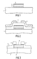
- This passivation layer 5 is deposited by PCVD (plasma activated chemical vapor deposition), as is the case e.g. is described in the above-mentioned reference "Solid State Technology", April l98l, l67 to l7l.
- the passivation layer 5 is then covered in a conventional manner with a photoresist mask 6, which, as shown in FIG. 2, contains an opening 7 through which the passivation layer 5 and the adhesive layer 4 are exposed by a suitable etching method (for example chemical etching or sputter etching) Surface 8 of the metallization layer 2 are removed.
- a suitable etching method for example chemical etching or sputter etching
Landscapes
- Formation Of Insulating Films (AREA)
- Internal Circuitry In Semiconductor Integrated Circuit Devices (AREA)
- Die Bonding (AREA)
- Local Oxidation Of Silicon (AREA)
Abstract
Description
- Die Erfindung betrifft ein Verfahren zum Herstellen von Halbleiter-Bauelementen, bei dem eine Oberfläche des Halbleiterkörpers und darauf angebrachte Metallisierungsschichten aus Gold mit einer Passivierungsschicht aus Siliziumnitrid bedeckt werden.
- Das Bedecken der Oberfläche von Halbleiterkörpern mit einer durch PCVD (plasma activated chemical vapor deposition) niedergeschlagenen Schicht ist z. B. aus "Solid State Technology", April l98l, l67 bis l7l bekannt. Befinden sich auf der mit der Passivierungsschicht bedeckten Oberfläche des Halbleiterkörpers Metallisierungsschichten, so werden diese zunächst von der Passivierungsschicht mit bedeckt, die dann an den Stellen, an denen die Metallisierungsschicht kontaktiert werden sollen entfernt werden.
Bestehen diese Metallisierungsschichten aus Gold, so zeigt sich, daß die Haftung der Passivierungsschicht aus Siliziumnitrid auf ihnen nicht sehr gut ist und die Gefahr besteht, daß die Passivierungsschicht beim Freilegen der Metallisierungsschichten, z. B. durch Ätzen, teilweise abblättert. - Bei einem Verfahren der eingangs genannten Art ist daher die Ausbeute erheblich herabgesetzt.
Der Erfindung liegt daher die Aufgabe zugrunde dieses Verfahren so weiter zu bilden, daß die Haftung der Passivierungsschicht aus Siliziumnitrid auf den Metallisierungsschichten aus Gold wesentlich erhöht werden. - Diese Aufgabe wird erfindungsgemäß dadurch gelöst, daß vor dem Aufbringen der Nitridschicht, auf die Metallisierungsschichten eine Haftschicht aus einem oder mehreren der Metalle W, Ti und Mo in einer N₂-haltigen Atmosphäre aufgeputtert wird.
- Eine solche Haftschicht zwischen den Metallisierungsschichten aus Gold und der Passivierungsschicht aus Siliziumnitrid führt zu einer sehr guten Haftung, so daß beim Ätzen der Passivierungsschicht kein Ablösen mehr zu befürchten ist.
- Weitere Ausgestaltung der Erfindung ergeben sich aus den Unteransprüchen.
- Für ein Ausführungsbeispiel der Erfindung wird im folgenden anhand der beigefügten Zeichnung mehr erläutert.
- Die Fig. l bis 3 zeigen jeweils einen Ausschnitt aus einem Halbleiter-Bauelement das mit dem Verfahren nach der Erfindung hergestellt wird, in aufeinander folgenden Stufen seiner Herstellung.
- Figur l zeigt einen Halbleiterkörper l aus z. B. Silizium auf dessen einer Oberfläche eine Metallisierungsschicht 2 aus Gold angebracht ist. Die Dicke dieser Metallisierungsschicht beträgt etwa 0,6 µm.
Sie liegt nicht unmittelbar auf der Oberfläche sondern auf einer die Haftung verbessernden Schicht 3, die aus WTi (90 %W l0 %Ti) besteht und eine Dicke von 0,4 µm hat. Die Oberfläche der Metallisierungsschicht 2 ist mit einer Haftschicht 4 bedeckt, die in den hier beschriebenen Ausführungsbeispiel aus WTi (90%W, l0 %Ti) besteht und deren Dicke etwa 50 nm beträgt. - Die Haftschicht 4 wird auf die Metallisierungsschicht 2 aufgesputtert und zwar in einer N₂-haltigen Atmophäre um so eine Legierungsbildung zwischen dem Gold der Metallisierungsschicht und dem WTi der Haftschicht zu vermeiden. Der beim Aufputtern üblicherweise verwendeten Inertatmosphäre aus Argon ist etwa 30 Vol.% N₂ beigefügt.
- Die Oberfläche des Halbleiterkörpers l mit der darauf liegenden Metallisierungsschicht 2 die von der Haftschicht 4 bedeckt ist wird nun - wie es die Figur 2 zeigt - mit einer Passivierungsschicht 5 aus Siliziumnitrid bedeckt. Diese Passivierungsschicht 5 wird durch PCVD (plasma activated chemical vapor deposition) niedergeschlagen wie dies z.B. in der oben bereits genannten Literaturstelle "Solid State Technology", April l98l, l67 bis l7l beschrieben ist.
- Die Dicke der Nitridschicht beträgt etwa l µm.
- Anschließend wird die Passivierungsschicht 5 auf übliche Art und Weise mit einer Fotolackmaske 6 bedeckt, die wie in Figur 2 dargestellt eine Öffnung 7 enthält durch die hindurch durch ein geeignetes Ätzverfahren (z.B. chemisches Ätzen oder Sputterätzen) die Passivierungsschicht 5 und die Haftschicht 4 über einer freizulegenden Fläche 8 der Metallisierungsschicht 2 entfernt werden. An dieser Fläche 8 kann dann die Metallisierungsschicht 2 auf geeignete Weise kontaktiert werden.
- Das Entfernen der beiden genannten Schichten geschieht vorzugsweise durch reaktives Sputterätzen. Das vollständige Entfernen beider Schichten kann leicht optisch kontrolliert werden, da nach dem vollständigen Entfernen der Haftschicht 4 eine deutliche Farbänderung von der grauen Haftschicht zu dem gelbglänzenden Gold der Metallisierungsschicht auftritt.
Claims (7)
dadurch gekennzeichnet, daß die Passivierungsschicht durch PCVD (plasma activated chemical vapor deposition) niedergeschlagen wird.
dadurch gekennzeichnet, daß die Haftschicht mit einer Dicke kleiner als l00 nm aufgebracht wird.
dadurch gekennzeichnet, daß die Haftschicht mit einer Dicke von etwa 50 nm aufgebracht wird.
dadurch gekennzeichnet, daß die Haftschicht aus l0 Gew.% Ti und 90 Gew.% W besteht.
dadurch gekennzeichnet, daß die Haftschicht aus Ti besteht.
dadurch gekennzeichnet, daß die Haftschicht in einer 30Vol.% N₂ enthaltenden Atmosphäre aufgeputtert wird.
Applications Claiming Priority (2)
| Application Number | Priority Date | Filing Date | Title |
|---|---|---|---|
| DE19863610709 DE3610709A1 (de) | 1986-03-29 | 1986-03-29 | Verfahren zum herstellen von halbleiter-bauelementen |
| DE3610709 | 1986-03-29 |
Publications (3)
| Publication Number | Publication Date |
|---|---|
| EP0240070A2 true EP0240070A2 (de) | 1987-10-07 |
| EP0240070A3 EP0240070A3 (en) | 1990-04-25 |
| EP0240070B1 EP0240070B1 (de) | 1992-10-21 |
Family
ID=6297572
Family Applications (1)
| Application Number | Title | Priority Date | Filing Date |
|---|---|---|---|
| EP87200532A Expired - Lifetime EP0240070B1 (de) | 1986-03-29 | 1987-03-23 | Verfahren zum Herstellen von Halbleiter-Bauelementen |
Country Status (3)
| Country | Link |
|---|---|
| EP (1) | EP0240070B1 (de) |
| JP (1) | JPS62272557A (de) |
| DE (2) | DE3610709A1 (de) |
Families Citing this family (3)
| Publication number | Priority date | Publication date | Assignee | Title |
|---|---|---|---|---|
| JPS644047A (en) * | 1987-06-26 | 1989-01-09 | Toshiba Corp | Semiconductor device |
| JP2558932B2 (ja) * | 1990-07-24 | 1996-11-27 | 松下電器産業株式会社 | 化合物半導体集積回路 |
| JP2007250814A (ja) * | 2006-03-16 | 2007-09-27 | Nippon Telegr & Teleph Corp <Ntt> | 配線構造とその製造方法 |
Family Cites Families (7)
| Publication number | Priority date | Publication date | Assignee | Title |
|---|---|---|---|---|
| US3900944A (en) * | 1973-12-19 | 1975-08-26 | Texas Instruments Inc | Method of contacting and connecting semiconductor devices in integrated circuits |
| US4300149A (en) * | 1979-09-04 | 1981-11-10 | International Business Machines Corporation | Gold-tantalum-titanium/tungsten alloy contact for semiconductor devices and having a gold/tantalum intermetallic barrier region intermediate the gold and alloy elements |
| JPS5848459A (ja) * | 1981-09-16 | 1983-03-22 | Nec Corp | 半導体装置 |
| JPS5860535A (ja) * | 1981-10-06 | 1983-04-11 | Nec Corp | 多層電極の製造方法 |
| JPS59198734A (ja) * | 1983-04-25 | 1984-11-10 | Mitsubishi Electric Corp | 多層配線構造 |
| JPS60103668A (ja) * | 1983-11-10 | 1985-06-07 | Nec Corp | 半導体装置 |
| JPS60119755A (ja) * | 1983-12-01 | 1985-06-27 | Nec Corp | 多層配線半導体集積回路装置 |
-
1986
- 1986-03-29 DE DE19863610709 patent/DE3610709A1/de not_active Withdrawn
-
1987
- 1987-03-23 EP EP87200532A patent/EP0240070B1/de not_active Expired - Lifetime
- 1987-03-23 DE DE8787200532T patent/DE3782264D1/de not_active Expired - Lifetime
- 1987-03-27 JP JP62071911A patent/JPS62272557A/ja active Pending
Also Published As
| Publication number | Publication date |
|---|---|
| JPS62272557A (ja) | 1987-11-26 |
| EP0240070A3 (en) | 1990-04-25 |
| DE3782264D1 (de) | 1992-11-26 |
| EP0240070B1 (de) | 1992-10-21 |
| DE3610709A1 (de) | 1987-10-08 |
Similar Documents
| Publication | Publication Date | Title |
|---|---|---|
| DE3853392T2 (de) | Verbindungsstruktur eines Halbleiterbauelementes und Verfahren zu ihrer Herstellung. | |
| DE2617914C2 (de) | Verfahren zum Herstellen von Mustern eines dünnen Films auf einem Substrat bei der Herstellung von integrierten Schaltungen | |
| DE2448535C2 (de) | Verfahren zum Niederschlagen dünner leitfähiger Filme auf einem anorganischen Substrat | |
| DE2402709C3 (de) | Festkörperbauelement mit einem dünnen Film aus Vanadinoxyd | |
| DE1907740A1 (de) | Halbleiteranordnung mit einem wenigstens zwei Halbleiterbereiche entgegengesetzten Leitungstype aufweisenden Halbleiterkoerper | |
| DE3414781A1 (de) | Vielschicht-verbindungsstruktur einer halbleitereinrichtung | |
| DE2432719A1 (de) | Verfahren zum erzeugen von feinen strukturen aus aufdampfbaren materialien auf einer unterlage | |
| DE2202520A1 (de) | Metall-Isolieraufbau | |
| DE68922085T2 (de) | Halbleiteranordung und Verfahren zum Herstellen einer Halbleiteranordung. | |
| DE3634168A1 (de) | Halbleitereinrichtung und herstellungsverfahren dafuer | |
| DE69030400T2 (de) | Anordnung der Rückseitenmetallisierung für Halbleiterbauelemente | |
| DE69017520T2 (de) | Metallisierungsprozess. | |
| EP0240070A2 (de) | Verfahren zum Herstellen von Halbleiter-Bauelementen | |
| EP0105189B1 (de) | Verfahren zum Herstellen von Metallelektroden unterschiedlicher Dicke für Halbleiterbauelemente, insbesondere für Leistungshalbleiterbauelemente wie Thyristoren | |
| DE2754526A1 (de) | Verfahren zur herstellung einer fotokathode fuer elektroradiographische und elektrofluoroskopische apparate | |
| DE69321265T2 (de) | Verfahren zur Herstellung einer Höckerkontaktstruktur auf einer Halbleiteranordnung | |
| EP0967296B1 (de) | Verfahren zum Beschichten eines Substrats | |
| DE19528441A1 (de) | Untermetallisierung für Lotmaterialien | |
| DE1764937C3 (de) | Verfahren zur Herstellung von Isolationsschichten zwischen mehrschichtig übereinander angeordneten metallischen Leitungsverbindungen für eine Halbleiteranordnung | |
| DE4328067C1 (de) | Verfahren zum Aufbringen von metallischen Schichten auf einem nichtmetallischen Substrat unter Einsatz eines Haftvermittlers | |
| DE1942455C3 (de) | Verfahren zum Herstellen mehrschichtiger Leiterbahnen | |
| DE3227898A1 (de) | Schichtsystem fuer optoelektronische anzeigen | |
| EP0361572A1 (de) | Verfahren zum Herstellen von Leiterbahnen auf Halbleiterbauelementen | |
| EP0211168B1 (de) | Verfahren zum Herstellen einer Durchsichtphotokathode | |
| DE2058554B2 (de) | Verfahren zur herstellung von chrom-halbleiterkontakten |
Legal Events
| Date | Code | Title | Description |
|---|---|---|---|
| PUAI | Public reference made under article 153(3) epc to a published international application that has entered the european phase |
Free format text: ORIGINAL CODE: 0009012 |
|
| AK | Designated contracting states |
Kind code of ref document: A2 Designated state(s): DE FR GB IT |
|
| PUAL | Search report despatched |
Free format text: ORIGINAL CODE: 0009013 |
|
| AK | Designated contracting states |
Kind code of ref document: A3 Designated state(s): DE FR GB IT |
|
| 17P | Request for examination filed |
Effective date: 19901023 |
|
| 17Q | First examination report despatched |
Effective date: 19920115 |
|
| GRAA | (expected) grant |
Free format text: ORIGINAL CODE: 0009210 |
|
| AK | Designated contracting states |
Kind code of ref document: B1 Designated state(s): DE FR GB IT |
|
| ITF | It: translation for a ep patent filed | ||
| REF | Corresponds to: |
Ref document number: 3782264 Country of ref document: DE Date of ref document: 19921126 |
|
| GBT | Gb: translation of ep patent filed (gb section 77(6)(a)/1977) |
Effective date: 19930106 |
|
| ET | Fr: translation filed | ||
| PLBE | No opposition filed within time limit |
Free format text: ORIGINAL CODE: 0009261 |
|
| STAA | Information on the status of an ep patent application or granted ep patent |
Free format text: STATUS: NO OPPOSITION FILED WITHIN TIME LIMIT |
|
| 26N | No opposition filed | ||
| ITTA | It: last paid annual fee | ||
| PGFP | Annual fee paid to national office [announced via postgrant information from national office to epo] |
Ref country code: GB Payment date: 19950228 Year of fee payment: 9 |
|
| PGFP | Annual fee paid to national office [announced via postgrant information from national office to epo] |
Ref country code: FR Payment date: 19950329 Year of fee payment: 9 |
|
| ITPR | It: changes in ownership of a european patent |
Owner name: CAMBIO RAGIONE SOCIALE;PHILIPS ELECTRONICS N.V. |
|
| PGFP | Annual fee paid to national office [announced via postgrant information from national office to epo] |
Ref country code: DE Payment date: 19950529 Year of fee payment: 9 |
|
| REG | Reference to a national code |
Ref country code: FR Ref legal event code: CD |
|
| PG25 | Lapsed in a contracting state [announced via postgrant information from national office to epo] |
Ref country code: GB Effective date: 19960323 |
|
| GBPC | Gb: european patent ceased through non-payment of renewal fee |
Effective date: 19960323 |
|
| PG25 | Lapsed in a contracting state [announced via postgrant information from national office to epo] |
Ref country code: FR Effective date: 19961129 |
|
| PG25 | Lapsed in a contracting state [announced via postgrant information from national office to epo] |
Ref country code: DE Effective date: 19961203 |
|
| REG | Reference to a national code |
Ref country code: FR Ref legal event code: ST |
|
| PG25 | Lapsed in a contracting state [announced via postgrant information from national office to epo] |
Ref country code: IT Free format text: LAPSE BECAUSE OF NON-PAYMENT OF DUE FEES;WARNING: LAPSES OF ITALIAN PATENTS WITH EFFECTIVE DATE BEFORE 2007 MAY HAVE OCCURRED AT ANY TIME BEFORE 2007. THE CORRECT EFFECTIVE DATE MAY BE DIFFERENT FROM THE ONE RECORDED. Effective date: 20050323 |