EP0225821A2 - Dispositif semi-conducteur à structure silicium sur isolant - Google Patents
Dispositif semi-conducteur à structure silicium sur isolant Download PDFInfo
- Publication number
- EP0225821A2 EP0225821A2 EP86402417A EP86402417A EP0225821A2 EP 0225821 A2 EP0225821 A2 EP 0225821A2 EP 86402417 A EP86402417 A EP 86402417A EP 86402417 A EP86402417 A EP 86402417A EP 0225821 A2 EP0225821 A2 EP 0225821A2
- Authority
- EP
- European Patent Office
- Prior art keywords
- region
- contact
- type
- insular
- semiconductor device
- Prior art date
- Legal status (The legal status is an assumption and is not a legal conclusion. Google has not performed a legal analysis and makes no representation as to the accuracy of the status listed.)
- Granted
Links
- 239000004065 semiconductor Substances 0.000 title claims abstract description 67
- 239000012212 insulator Substances 0.000 title claims abstract description 53
- 229910052710 silicon Inorganic materials 0.000 title claims description 20
- 239000010703 silicon Substances 0.000 title claims description 20
- 239000012535 impurity Substances 0.000 claims abstract description 16
- 229910021421 monocrystalline silicon Inorganic materials 0.000 claims abstract description 14
- XUIMIQQOPSSXEZ-UHFFFAOYSA-N Silicon Chemical compound [Si] XUIMIQQOPSSXEZ-UHFFFAOYSA-N 0.000 claims description 19
- 230000005669 field effect Effects 0.000 claims description 2
- 229910044991 metal oxide Inorganic materials 0.000 claims description 2
- 150000004706 metal oxides Chemical class 0.000 claims description 2
- 108091006146 Channels Proteins 0.000 description 23
- VYPSYNLAJGMNEJ-UHFFFAOYSA-N Silicium dioxide Chemical compound O=[Si]=O VYPSYNLAJGMNEJ-UHFFFAOYSA-N 0.000 description 10
- 239000000758 substrate Substances 0.000 description 9
- 239000005360 phosphosilicate glass Substances 0.000 description 8
- 230000015572 biosynthetic process Effects 0.000 description 6
- 235000012239 silicon dioxide Nutrition 0.000 description 5
- 239000000377 silicon dioxide Substances 0.000 description 5
- 238000000034 method Methods 0.000 description 3
- 229910021420 polycrystalline silicon Inorganic materials 0.000 description 3
- 229920005591 polysilicon Polymers 0.000 description 3
- 108010075750 P-Type Calcium Channels Proteins 0.000 description 2
- 239000013078 crystal Substances 0.000 description 2
- 238000009792 diffusion process Methods 0.000 description 2
- 230000010354 integration Effects 0.000 description 2
- 150000002500 ions Chemical class 0.000 description 2
- 230000003213 activating effect Effects 0.000 description 1
- 230000015556 catabolic process Effects 0.000 description 1
- 238000005229 chemical vapour deposition Methods 0.000 description 1
- 230000000694 effects Effects 0.000 description 1
- 230000001678 irradiating effect Effects 0.000 description 1
- 238000002955 isolation Methods 0.000 description 1
- 239000002184 metal Substances 0.000 description 1
- 238000000059 patterning Methods 0.000 description 1
- 229910052594 sapphire Inorganic materials 0.000 description 1
- 239000010980 sapphire Substances 0.000 description 1
Images


Classifications
-
- H—ELECTRICITY
- H01—ELECTRIC ELEMENTS
- H01L—SEMICONDUCTOR DEVICES NOT COVERED BY CLASS H10
- H01L29/00—Semiconductor devices adapted for rectifying, amplifying, oscillating or switching, or capacitors or resistors with at least one potential-jump barrier or surface barrier, e.g. PN junction depletion layer or carrier concentration layer; Details of semiconductor bodies or of electrodes thereof ; Multistep manufacturing processes therefor
- H01L29/66—Types of semiconductor device ; Multistep manufacturing processes therefor
- H01L29/68—Types of semiconductor device ; Multistep manufacturing processes therefor controllable by only the electric current supplied, or only the electric potential applied, to an electrode which does not carry the current to be rectified, amplified or switched
- H01L29/76—Unipolar devices, e.g. field effect transistors
- H01L29/772—Field effect transistors
- H01L29/78—Field effect transistors with field effect produced by an insulated gate
- H01L29/786—Thin film transistors, i.e. transistors with a channel being at least partly a thin film
- H01L29/78606—Thin film transistors, i.e. transistors with a channel being at least partly a thin film with supplementary region or layer in the thin film or in the insulated bulk substrate supporting it for controlling or increasing the safety of the device
- H01L29/78612—Thin film transistors, i.e. transistors with a channel being at least partly a thin film with supplementary region or layer in the thin film or in the insulated bulk substrate supporting it for controlling or increasing the safety of the device for preventing the kink- or the snapback effect, e.g. discharging the minority carriers of the channel region for preventing bipolar effect
- H01L29/78615—Thin film transistors, i.e. transistors with a channel being at least partly a thin film with supplementary region or layer in the thin film or in the insulated bulk substrate supporting it for controlling or increasing the safety of the device for preventing the kink- or the snapback effect, e.g. discharging the minority carriers of the channel region for preventing bipolar effect with a body contact
-
- Y—GENERAL TAGGING OF NEW TECHNOLOGICAL DEVELOPMENTS; GENERAL TAGGING OF CROSS-SECTIONAL TECHNOLOGIES SPANNING OVER SEVERAL SECTIONS OF THE IPC; TECHNICAL SUBJECTS COVERED BY FORMER USPC CROSS-REFERENCE ART COLLECTIONS [XRACs] AND DIGESTS
- Y10—TECHNICAL SUBJECTS COVERED BY FORMER USPC
- Y10S—TECHNICAL SUBJECTS COVERED BY FORMER USPC CROSS-REFERENCE ART COLLECTIONS [XRACs] AND DIGESTS
- Y10S257/00—Active solid-state devices, e.g. transistors, solid-state diodes
- Y10S257/901—MOSFET substrate bias
Definitions
- the present invention generally relates to semiconductor devices having a silicon on insulator structure, and more particularly to a semiconductor device having a silicon on insulator structure with stable electrical characteristics.
- a known semiconductor device having a silicon on insulator (hereinafter simply referred to as an SOI) structure is produced by forming a relatively thick insulator layer on a semiconductor substrate, forming a polysilicon layer on the insulator layer by chemical vapor deposition, forming the polysilicon layer into a single crystal silicon layer by irradiating an energy beam or the like, forming an insular single crystal silicon body by a patterning process, and forming a semiconductor device on the insular single crystal silicon body.
- SOI silicon on insulator
- a semiconductor integrated circuit (IC) including high voltage elements can be easily formed because the isolation between elements is positively provided.
- the integration density of the semiconductor IC can be improved by employing a three-dimentional structure.
- MIS metal insulator semiconductor
- the impurity density of the insular body may be set to a high value, but this method is impractical in that the current gain becomes greatly reduced.
- the crystal property of the insular single crystal silicon body formed on the insulator layer of the SOI structure is deteriorated compared to that of a silicon substrate which is generally used.
- the diffusion rate of impurities is extremely fast for the insular single crystal silicon body compared to that of the silicon substrate, and it is difficult to limit the depth of the impurity diffusion region under the thickness of the insular single crystal silicon body.
- MOS Metal oxide semiconductor
- an insular p-type silicon body is formed on an insulating substrate made of sapphire, for example.
- An n+-type source region and a p-type channel region adjacent thereto are provided in the insular body down to a boundary between the insulating substrate and the insular body.
- An n+-type drain region is provided in the surface portion of the channel region, at a position separated from the source region.
- a p+-type impurity region is provided adjacent to the channel region and the drain region down to the boundary.
- a gate electrode is provided on the channel region via a gate insulator layer.
- the thickness of the insular body is in the order of one micron
- the thickness of the drain region provided in the surface portion of the channel region is in the order of 0.2 micron.
- a semiconductor device having an insulator layer; an insular body formed on the insulator layer, the insular body being made of a single crystal silicon doped to a first type semiconductor; a first region of the first type semiconductor provided in the insular body; first and second doped regions of a second type semiconductor provided in the insular body on both sides of the first region, the first and second doped regions reaching a bottom of the insular body and having a width smaller than a width of the insular body; a second region of the first type semiconductor in contact with the first region and formed along a side of the source and drain regions; and a contact region of the first type semiconductor formed in contact with the second region and having an impurity density higher than those of the first and second regions, so that a fixed voltage can be applied to the first region via the contact region.
- the semiconductor device having the SOI structure of the present invention makes it possible to easily apply a fixed voltage to the insular body of the semiconductor device. According to the present invention, it is thus possible, without reducing the current gain, to prevent the formation of a back channel which would cause a leakage current to flow between the source and the drain. Hence, it is possible to improve the stability and performance of elements on the semiconductor device and, accordingly, to stabilize the electrical characteristics of the semiconductor device.
- An insulator layer 12 is formed on a silicon substrate 11, and an insular p-type single crystal silicon body 13 is provided on the insulator layer 12.
- An n+-type source region 14, and n+-type drain region 15 and a channel region 16 are formed in the insular body 13.
- a gate insulator layer 17 is formed on the channel region 16, and a gate electrode 18 is formed on the gate insulator layer 17.
- An oxide layer 19 is formed on the gate electrode 18, and a phospho-silicate glass (PSG) insulator layer 20 is formed on the oxide layer 19.
- Contact holes 21 are formed in the oxide layer 19 and the PSG insulator layer 20, and a gate wiring 22, a source wiring 23 and a drain wiring 24 are provided to make the necessary contact through the respective contact holes 21 as shown.
- the source and drain regions 14 and 15 are formed by selectively implanting n-type impurity ions into the insular body 13 by using the gate electrode 18 as a mask and thereafter activating the regions implanted with the impurity ions.
- the source and drain regions 14 and 15 inevitably reach the bottom of the insular body 13. In other words, the source and drain regions 14 and 15 reach a boundary between the insulator layer 12 and the insular body 13.
- the source region 14 prevents the contact region 25 from being electrically connected to the insular body 13 under the gate electrode 18. For this reason, it is impossible to apply a fixed voltage to the insular body 13 (channel region 16) via the contact region 25. As a result, the conventional MIS device having the SOI structure has no contact for applying the fixed voltage to the insular body 13.
- the insular body 13 is in a floating state, and a leakage current is easily generated between the source region 14 and the drain region 15 due to a back channel at a lower portion of the insular body 13.
- the electrical characteristic of the MIS device is unstable.
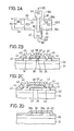
- Figs.2A through 2D show a first embodiment of a semiconductor device having a SOI structure according to the present invention.
- a silicon dioxide (SiO2) insulator layer 32 having a thickness in the order of one micron is formed on a silicon substrate 31, and an insular p ⁇ -type single crystal silicon body 33 having an impurity density in the range of 1014 to 1016 cm ⁇ 3 and a thickness of 0.5 micron is provided on the SiO2 insulator layer 32.
- SiO2 insulator layer 32 having a thickness in the order of one micron is formed on a silicon substrate 31, and an insular p ⁇ -type single crystal silicon body 33 having an impurity density in the range of 1014 to 1016 cm ⁇ 3 and a thickness of 0.5 micron is provided on the SiO2 insulator layer 32.
- n+-type source region 34 having an impurity density in the order of 1020 cm ⁇ 3, and n+-type drain region 35 having an impurity density in the order of 1020 cm ⁇ 3 and a p ⁇ -type channel region (hereinafter referred to as a first p ⁇ -type region) 36 are formed in the insular body 33.
- a SiO2 gate insulator layer 37 is formed on the first p ⁇ -type region 36, and a polysilicon gate electrode 38 is formed on the gate insulator layer 37.
- Second p ⁇ -type regions 39a and 39b are respectively provided along the sides of the source and drains regions 34 and 35.
- a p+-type contact region 40 having an impurity density in the order of 1020cm ⁇ 3 is provided adjacent to the second p ⁇ -type region 39a in contact therewith.
- Fig. 2C shows that an end portion of the gate insulator layer 37 overlaps a portion of the contact region 40.
- a SiO2 oxide layer 41 is formed on the gate electrode 38, and a PSG insulator layer 42 is formed on the oxide layer 41.
- Contact holes 43 are formed in the oxide layer 41 and the PSG insulator layer 42, and a gate wiring 44, a source wiring 45, a drain wiring 46 and a contact wiring 47 are provided to make the necessary contacts through the respective contact holes 43 as shown.
- the impurity density of the contact region 40 is higher than those of the first and second p ⁇ -type regions 36 and 39a and 39b.
- a fixed voltage such as a ground potential from the contact wiring 47 is applied to the insular body 33, that is, to the first p ⁇ -type region 36 wherein the channel is formed, via the contact region 40.
- the contact region 40 also functions as a channel stopper.
- the n+-type source and drain regions 34 and 35 are formed so that a width W1 thereof is smaller than a width W2 of the insular p ⁇ -type single crystal body 33, and the second p ⁇ -type regions 39a and 39b which are in contact with the first p ⁇ -type region 36 are formed along the sides of the n+-type source and drain regions 34 and 35.
- the p+-type contact region 40 is formed in contact with the second p ⁇ -type region 39a.
- the p+-type contact region 40 and the first p ⁇ -type region 36 wherein the channel is formed are electrically connected without being blocked by the n+-type source and drain regions 34 and 35 which reach the bottom of the insular body 33.
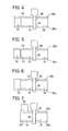
- Figs.3A through 3C those parts which are the same as corresponding parts in Figs.2A through 2D are designated by the same reference numerals, and the description thereof will be omitted.
- the second embodiment only differs from the first embodiment described before in the a p+-type contact region 50 is formed in contact with the second p ⁇ -type region 39a at a position separated from the gate electrode 38 in the plan view, the contact region 50 not being in contact with the gate insulator layer.
- the effects of the second embodiment are basically the same as those of the first embodiment, except that the contact region 50 does not function as a channel stopper as in the case of the contact region 40.
- Figs.4 through 7 those parts which are the same as those corresponding parts in Figs.2A through 2D are designated by the same reference numerals, and the description thereof will be omitted.
- a p+-type contact region 52 is formed adjacent to the n+-type source region 34.
- the second p ⁇ -type regions 39a and 39b extend along the sides of the n+-type source and drain regions 34 and 35 and the sides of the p+-type contact region 52.
- the p+-type contact region 52 is in contact with the second p ⁇ -type regions 39a and 39b, and the p+-type contact region 52 and the first p ⁇ -type region 36 wherein the channel is formed are electrically connected without being blocked by the n+-type source and drain regions 34 and 35 which reach the bottom of the insular body 33.
- the source potential is approximately equal to the potential of the insular body or is lower than the drain potential. For this reason, it is possible to more positively prevent a breakdown at the junction when the contact region is formed adjacent to the source region rather than adjacent to the drain region.
- the fourth embodiment shown in Fig.5 is basically the same as the third embodiment except that an insulator layer 53 which reaches the bottom of the insular body 33 is provided between the p+-type contact region 52 and the n+-type source region 34.
- a p+-type contact region 54 is formed adjacent to the n+-type source region 34.
- the p+-type contact region 54 is in contact with the end portions of the second p ⁇ -type regions 39a and 39b, and the p+-type contact region 54 and the first p ⁇ -type region 36 wherein the channel is formed are electrically connected without being blocked by the n+-type source and drain regions 34 and 35 which reach the bottom of the insular body 33.
- the sixth embodiment shown in Fig. 7 is basically the same as the second embodiment except that a p+-type contact region 55 is formed adjacent to the second p ⁇ -type region 39b in contact therewith.
- the p+-type contact region 55 and the first p ⁇ -type region 36 wherein the channel is formed are electrically connected without being blocked by the n+-type source and drain regions 34 and 35 which reach the bottom of the insular body 33.
- the location of the contact region may be selected arbitrarily according to the arrangement of the elements on the semiconductor device, so that it is possible to improve the integration density.
- the insular body 33 to which a fixed voltage is to be applied is a p ⁇ -type body.
- the present invention to a semiconductor device having a SOI structure in which an n-type insular body is to be applied with the fixed voltage.
- the second p ⁇ -type regions 39a and 39b are formed along both sides of the n+-type source and drain regions 34 and 35, but it is also possible to provide a single second p ⁇ -type region along only one side of the source and drain regions 34 and 35.
- the p+-type contact region must of course be in contact with the first p ⁇ -type region 36 and be formed in contact with the single second p ⁇ -type region.
- the second p ⁇ -type regions 39a and 39b are formed along both sides of the source and drain regions 34 and 35, there are advantages in that the widths of the source and drain regions 34 and 35 are restricted by self-alignment, and the characteristics of the semiconductor device will not change even when there is a positioning error of the gate electrode 38 when the semiconductor is produced. Furthermore, with the embodiments described heretofore, the p+-type contact region will not make contact with junctions between the first p ⁇ -type region (channel region) 36 and the source and drain regions 34 and 35 and a short circuit will not occur, even when the width of the gate electrode 38 is narrow.
- the application of the present invention is not limited to the formation of the contact region for MIS field effect transistor (FET) formed on a semiconductor device having a SOI structure, and it is possible to apply the present invention to the formation of a base contact for a bipolar transistor formed on a semiconductor device having a SOI structure, such as a lateral npn transistor and a lateral pnp transistor.
- FET field effect transistor
Applications Claiming Priority (2)
| Application Number | Priority Date | Filing Date | Title |
|---|---|---|---|
| JP244433/85 | 1985-10-31 | ||
| JP60244433A JPS62104173A (ja) | 1985-10-31 | 1985-10-31 | 半導体装置 |
Publications (3)
| Publication Number | Publication Date |
|---|---|
| EP0225821A2 true EP0225821A2 (fr) | 1987-06-16 |
| EP0225821A3 EP0225821A3 (en) | 1988-01-13 |
| EP0225821B1 EP0225821B1 (fr) | 1992-01-02 |
Family
ID=17118582
Family Applications (1)
| Application Number | Title | Priority Date | Filing Date |
|---|---|---|---|
| EP86402417A Expired - Lifetime EP0225821B1 (fr) | 1985-10-31 | 1986-10-29 | Dispositif semi-conducteur à structure silicium sur isolant |
Country Status (5)
| Country | Link |
|---|---|
| US (1) | US4809056A (fr) |
| EP (1) | EP0225821B1 (fr) |
| JP (1) | JPS62104173A (fr) |
| KR (1) | KR900000097B1 (fr) |
| DE (1) | DE3683263D1 (fr) |
Cited By (16)
| Publication number | Priority date | Publication date | Assignee | Title |
|---|---|---|---|---|
| EP0315424A2 (fr) * | 1987-11-05 | 1989-05-10 | Marconi Electronic Devices Limited | Dispositif pour transistor in effet de champ |
| FR2648623A1 (fr) * | 1989-06-19 | 1990-12-21 | France Etat | Structure de transistor mos sur isolant avec prise de caisson reliee a la source et procede de fabrication |
| FR2663464A1 (fr) * | 1990-06-19 | 1991-12-20 | Commissariat Energie Atomique | Circuit integre en technologie silicium sur isolant comportant un transistor a effet de champ et son procede de fabrication. |
| EP0479504A2 (fr) * | 1990-10-03 | 1992-04-08 | Mitsubishi Denki Kabushiki Kaisha | Transistor en couche mince |
| US5412240A (en) * | 1992-01-31 | 1995-05-02 | Canon Kabushiki Kaisha | Silicon-on-insulator CMOS device and a liquid crystal display with controlled base insulator thickness |
| US5434441A (en) * | 1992-01-31 | 1995-07-18 | Canon Kabushiki Kaisha | Silicon-on-insulator CMOS device and a liquid crystal display with controlled base insulator thickness |
| EP0690514A2 (fr) * | 1994-06-29 | 1996-01-03 | International Business Machines Corporation | Transistor SOI ayant un contact avec le substrat auto-aligné |
| EP0786813A1 (fr) * | 1994-09-30 | 1997-07-30 | Aktsionernoe Obschestvo Zakrytogo Tipa "Vl" | Transistor a effet de champ du type metal - dielectrique - semi-conducteur |
| EP0845815A2 (fr) * | 1996-11-28 | 1998-06-03 | Matsushita Electric Industrial Co., Ltd. | Dispositif semi-conducteur, méthode de conception, et dispositif de circuit intégré semi-conducteur |
| EP1540737A2 (fr) * | 2002-05-10 | 2005-06-15 | GENERAL SEMICONDUCTOR, Inc. | Dispositif a transistor mos a effet de champ presentant une geometrie qui permet un contact de corps frequent |
| EP2107613A1 (fr) * | 2008-03-27 | 2009-10-07 | Samsung Mobile Display Co., Ltd. | Transistor à couche mince, son procédé de fabrication, et dispositif d'affichage de diode électroluminescente organique l'incluant |
| EP2117048A2 (fr) * | 2008-04-11 | 2009-11-11 | Samsung Mobile Display Co., Ltd. | Transistor à couche mince, son procédé de fabrication, et dispositif d'affichage de diode électroluminescente organique l'incluant |
| EP2148362A1 (fr) * | 2008-07-22 | 2010-01-27 | Honeywell International Inc. | Procédé pour un contact direct à une région de liaison présentant un agencement efficace de la surface |
| US8253141B2 (en) | 2008-07-14 | 2012-08-28 | Samsung Mobile Display Co., Ltd. | Thin film transistor, method of fabricating the same, and organic light emitting diode display device including the thin film transistor |
| US8283668B2 (en) | 2007-08-23 | 2012-10-09 | Samsung Display Co., Ltd. | Thin film transistor, method of fabricating the same, and organic light emitting diode display device including the same |
| US8513669B2 (en) | 2007-08-22 | 2013-08-20 | Samsung Display Co., Ltd. | Thin film transistor including metal or metal silicide structure in contact with semiconductor layer and organic light emitting diode display device having the thin film transistor |
Families Citing this family (62)
| Publication number | Priority date | Publication date | Assignee | Title |
|---|---|---|---|---|
| US5248630A (en) * | 1987-07-27 | 1993-09-28 | Nippon Telegraph And Telephone Corporation | Thin film silicon semiconductor device and process for producing thereof |
| JPH07114184B2 (ja) * | 1987-07-27 | 1995-12-06 | 日本電信電話株式会社 | 薄膜形シリコン半導体装置およびその製造方法 |
| US5168337A (en) * | 1988-02-19 | 1992-12-01 | Nippondenso Co., Ltd. | Polycrystalline diode and a method for making the same |
| US4906587A (en) * | 1988-07-29 | 1990-03-06 | Texas Instruments Incorporated | Making a silicon-on-insulator transistor with selectable body node to source node connection |
| US5001528A (en) * | 1989-01-31 | 1991-03-19 | The United States Of America As Represented By The Secretary Of The Air Force | Radiation hardened CMOS on SOI or SOS devices |
| US5264721A (en) * | 1989-04-29 | 1993-11-23 | Fujitsu Limited | Insulated-gate FET on an SOI-structure |
| US5210438A (en) * | 1989-05-18 | 1993-05-11 | Fujitsu Limited | Semiconductor resistance element and process for fabricating same |
| US5160989A (en) * | 1989-06-13 | 1992-11-03 | Texas Instruments Incorporated | Extended body contact for semiconductor over insulator transistor |
| US5160987A (en) * | 1989-10-26 | 1992-11-03 | International Business Machines Corporation | Three-dimensional semiconductor structures formed from planar layers |
| US5227318A (en) * | 1989-12-06 | 1993-07-13 | General Motors Corporation | Method of making a cubic boron nitride bipolar transistor |
| US5264296A (en) * | 1989-12-06 | 1993-11-23 | General Motors Corporation | Laser depositon of crystalline boron nitride films |
| US5330611A (en) * | 1989-12-06 | 1994-07-19 | General Motors Corporation | Cubic boron nitride carbide films |
| US5047356A (en) * | 1990-02-16 | 1991-09-10 | Hughes Aircraft Company | High speed silicon-on-insulator device and process of fabricating same |
| US5079604A (en) * | 1990-03-02 | 1992-01-07 | Texas Instruments Incorporated | SOI layout for low resistance gate |
| US5142350A (en) * | 1990-07-16 | 1992-08-25 | General Motors Corporation | Transistor having cubic boron nitride layer |
| US5232862A (en) * | 1990-07-16 | 1993-08-03 | General Motors Corporation | Method of fabricating a transistor having a cubic boron nitride layer |
| US5750000A (en) * | 1990-08-03 | 1998-05-12 | Canon Kabushiki Kaisha | Semiconductor member, and process for preparing same and semiconductor device formed by use of same |
| US5274260A (en) * | 1990-08-30 | 1993-12-28 | Nippon Steel Corporation | Semiconductor device |
| US5225356A (en) * | 1991-01-14 | 1993-07-06 | Nippon Telegraph & Telephone Corporation | Method of making field-effect semiconductor device on sot |
| JPH0521762A (ja) * | 1991-07-10 | 1993-01-29 | Mitsubishi Electric Corp | 電界効果型トランジスタを備えた半導体装置およびその製造方法 |
| US5293052A (en) * | 1992-03-23 | 1994-03-08 | Harris Corporation | SOT CMOS device having differentially doped body extension for providing improved backside leakage channel stop |
| US5821575A (en) * | 1996-05-20 | 1998-10-13 | Digital Equipment Corporation | Compact self-aligned body contact silicon-on-insulator transistor |
| JP3319975B2 (ja) * | 1997-05-08 | 2002-09-03 | 株式会社日立製作所 | 半導体素子及びそれを用いた液晶表示装置 |
| US6239649B1 (en) | 1999-04-20 | 2001-05-29 | International Business Machines Corporation | Switched body SOI (silicon on insulator) circuits and fabrication method therefor |
| JP3573056B2 (ja) * | 1999-07-16 | 2004-10-06 | セイコーエプソン株式会社 | 半導体装置、半導体ゲートアレイおよび電気光学装置および電子機器 |
| JP3589102B2 (ja) * | 1999-07-27 | 2004-11-17 | セイコーエプソン株式会社 | Soi構造のmos電界効果トランジスタ及びその製造方法 |
| US6395587B1 (en) | 2000-02-11 | 2002-05-28 | International Business Machines Corporation | Fully amorphized source/drain for leaky junctions |
| JP2002261292A (ja) * | 2000-12-26 | 2002-09-13 | Toshiba Corp | 半導体装置及びその製造方法 |
| US6804502B2 (en) | 2001-10-10 | 2004-10-12 | Peregrine Semiconductor Corporation | Switch circuit and method of switching radio frequency signals |
| US6777883B2 (en) * | 2002-04-10 | 2004-08-17 | Koninklijke Philips Electronics N.V. | Integrated LED drive electronics on silicon-on-insulator integrated circuits |
| KR100542986B1 (ko) * | 2003-04-29 | 2006-01-20 | 삼성에스디아이 주식회사 | 박막 트랜지스터, 상기 박막 트랜지스터 제조 방법 및 이를 이용한 표시장치 |
| KR100543004B1 (ko) * | 2003-09-18 | 2006-01-20 | 삼성에스디아이 주식회사 | 평판표시장치 |
| KR100501706B1 (ko) * | 2003-10-16 | 2005-07-18 | 삼성에스디아이 주식회사 | 게이트-바디콘택 박막 트랜지스터 |
| EP3570374B1 (fr) | 2004-06-23 | 2022-04-20 | pSemi Corporation | Extrémité avant rf intégrée |
| US7890891B2 (en) | 2005-07-11 | 2011-02-15 | Peregrine Semiconductor Corporation | Method and apparatus improving gate oxide reliability by controlling accumulated charge |
| US7910993B2 (en) | 2005-07-11 | 2011-03-22 | Peregrine Semiconductor Corporation | Method and apparatus for use in improving linearity of MOSFET's using an accumulated charge sink |
| USRE48965E1 (en) | 2005-07-11 | 2022-03-08 | Psemi Corporation | Method and apparatus improving gate oxide reliability by controlling accumulated charge |
| US20080076371A1 (en) * | 2005-07-11 | 2008-03-27 | Alexander Dribinsky | Circuit and method for controlling charge injection in radio frequency switches |
| US8742502B2 (en) | 2005-07-11 | 2014-06-03 | Peregrine Semiconductor Corporation | Method and apparatus for use in improving linearity of MOSFETs using an accumulated charge sink-harmonic wrinkle reduction |
| US9653601B2 (en) | 2005-07-11 | 2017-05-16 | Peregrine Semiconductor Corporation | Method and apparatus for use in improving linearity of MOSFETs using an accumulated charge sink-harmonic wrinkle reduction |
| KR100741976B1 (ko) * | 2005-08-25 | 2007-07-23 | 삼성에스디아이 주식회사 | 박막트랜지스터 및 그 제조 방법 |
| EP1837917A1 (fr) * | 2006-03-21 | 2007-09-26 | Semiconductor Energy Laboratory Co., Ltd. | Dispositif de mémoire à semi-conducteur non volatile |
| TWI416738B (zh) * | 2006-03-21 | 2013-11-21 | Semiconductor Energy Lab | 非揮發性半導體記憶體裝置 |
| EP1837900A3 (fr) * | 2006-03-21 | 2008-10-15 | Semiconductor Energy Laboratory Co., Ltd. | Dispositif de mémoire à semi-conducteur non volatile |
| US8022460B2 (en) * | 2006-03-31 | 2011-09-20 | Semiconductor Energy Laboratory Co., Ltd. | Nonvolatile semiconductor memory device |
| US7554854B2 (en) | 2006-03-31 | 2009-06-30 | Semiconductor Energy Laboratory Co., Ltd. | Method for deleting data from NAND type nonvolatile memory |
| US7732287B2 (en) * | 2006-05-02 | 2010-06-08 | Honeywell International Inc. | Method of forming a body-tie |
| KR100878284B1 (ko) * | 2007-03-09 | 2009-01-12 | 삼성모바일디스플레이주식회사 | 박막트랜지스터와 그 제조 방법 및 이를 구비한유기전계발광표시장치 |
| KR100875432B1 (ko) | 2007-05-31 | 2008-12-22 | 삼성모바일디스플레이주식회사 | 다결정 실리콘층의 제조 방법, 이를 이용하여 형성된박막트랜지스터, 그의 제조방법 및 이를 포함하는유기전계발광표시장치 |
| EP3958468B1 (fr) * | 2008-02-28 | 2024-01-31 | pSemi Corporation | Procédé et appareil destinés au réglage numérique d'un condensateur dans un dispositif à circuit intégré |
| GB2459667A (en) * | 2008-04-29 | 2009-11-04 | Sharp Kk | Thin film transistor and active matrix display |
| US8723260B1 (en) | 2009-03-12 | 2014-05-13 | Rf Micro Devices, Inc. | Semiconductor radio frequency switch with body contact |
| US9590674B2 (en) | 2012-12-14 | 2017-03-07 | Peregrine Semiconductor Corporation | Semiconductor devices with switchable ground-body connection |
| US20150236798A1 (en) | 2013-03-14 | 2015-08-20 | Peregrine Semiconductor Corporation | Methods for Increasing RF Throughput Via Usage of Tunable Filters |
| US9406695B2 (en) | 2013-11-20 | 2016-08-02 | Peregrine Semiconductor Corporation | Circuit and method for improving ESD tolerance and switching speed |
| US9831857B2 (en) | 2015-03-11 | 2017-11-28 | Peregrine Semiconductor Corporation | Power splitter with programmable output phase shift |
| US9948281B2 (en) | 2016-09-02 | 2018-04-17 | Peregrine Semiconductor Corporation | Positive logic digitally tunable capacitor |
| US10236872B1 (en) | 2018-03-28 | 2019-03-19 | Psemi Corporation | AC coupling modules for bias ladders |
| US10505530B2 (en) | 2018-03-28 | 2019-12-10 | Psemi Corporation | Positive logic switch with selectable DC blocking circuit |
| US10886911B2 (en) | 2018-03-28 | 2021-01-05 | Psemi Corporation | Stacked FET switch bias ladders |
| US11476849B2 (en) | 2020-01-06 | 2022-10-18 | Psemi Corporation | High power positive logic switch |
| CN113644135B (zh) | 2020-05-11 | 2023-08-15 | 联华电子股份有限公司 | 场效晶体管及其制造方法 |
Citations (3)
| Publication number | Priority date | Publication date | Assignee | Title |
|---|---|---|---|---|
| JPS5727069A (en) * | 1980-07-25 | 1982-02-13 | Toshiba Corp | Mos type simiconductor device |
| FR2496342A1 (fr) * | 1980-12-12 | 1982-06-18 | Tokyo Shibaura Electric Co | Dispositif semi-conducteur du type metal-oxyde-semi-conducteur et son procede de fabrication |
| FR2520556A1 (fr) * | 1982-01-28 | 1983-07-29 | Tokyo Shibaura Electric Co | Dispositif semi-conducteur forme sur un substrat isolant |
Family Cites Families (4)
| Publication number | Priority date | Publication date | Assignee | Title |
|---|---|---|---|---|
| JPS5727068A (en) * | 1980-07-25 | 1982-02-13 | Toshiba Corp | Mos type semiconductor device |
| JPS5837966A (ja) * | 1981-08-31 | 1983-03-05 | Toshiba Corp | Mos型半導体装置 |
| JPS58124243A (ja) * | 1982-01-21 | 1983-07-23 | Toshiba Corp | 半導体装置の製造方法 |
| JPH06105784B2 (ja) * | 1984-07-26 | 1994-12-21 | 株式会社日立製作所 | 半導体装置 |
-
1985
- 1985-10-31 JP JP60244433A patent/JPS62104173A/ja active Pending
-
1986
- 1986-10-23 KR KR1019860008890A patent/KR900000097B1/ko not_active IP Right Cessation
- 1986-10-24 US US06/922,907 patent/US4809056A/en not_active Expired - Fee Related
- 1986-10-29 DE DE8686402417T patent/DE3683263D1/de not_active Expired - Fee Related
- 1986-10-29 EP EP86402417A patent/EP0225821B1/fr not_active Expired - Lifetime
Patent Citations (3)
| Publication number | Priority date | Publication date | Assignee | Title |
|---|---|---|---|---|
| JPS5727069A (en) * | 1980-07-25 | 1982-02-13 | Toshiba Corp | Mos type simiconductor device |
| FR2496342A1 (fr) * | 1980-12-12 | 1982-06-18 | Tokyo Shibaura Electric Co | Dispositif semi-conducteur du type metal-oxyde-semi-conducteur et son procede de fabrication |
| FR2520556A1 (fr) * | 1982-01-28 | 1983-07-29 | Tokyo Shibaura Electric Co | Dispositif semi-conducteur forme sur un substrat isolant |
Non-Patent Citations (2)
| Title |
|---|
| IEEE TRANSACTIONS ON ELECTRON DEVICES, vol. ED-32, no. 2, February 1985, pages 253-257, IEEE, New York, US; Y. HOKARI et al.: "Characteristics of MOSFET prepared on Si/MgO.Al2O3/SiO2/Si structure" * |
| PATENT ABSTRACTS OF JAPAN, vol. 6, no. 95 (E-110)[973], 3rd June 1982; & JP-A-57 027 069 (TOKYO SHIBAURA DENKI K.K.) 13-02-1982 * |
Cited By (32)
| Publication number | Priority date | Publication date | Assignee | Title |
|---|---|---|---|---|
| EP0315424A2 (fr) * | 1987-11-05 | 1989-05-10 | Marconi Electronic Devices Limited | Dispositif pour transistor in effet de champ |
| EP0315424A3 (fr) * | 1987-11-05 | 1989-08-16 | Marconi Electronic Devices Limited | Dispositif pour transistor in effet de champ |
| FR2648623A1 (fr) * | 1989-06-19 | 1990-12-21 | France Etat | Structure de transistor mos sur isolant avec prise de caisson reliee a la source et procede de fabrication |
| EP0414618A1 (fr) * | 1989-06-19 | 1991-02-27 | France Telecom | Transistor MOS en couche mince avec la zone de canal reliée à la source et son procédé de fabrication |
| US5130770A (en) * | 1990-06-19 | 1992-07-14 | Brevatome | Integrated circuit in silicon on insulator technology comprising a field effect transistor |
| EP0462882A1 (fr) * | 1990-06-19 | 1991-12-27 | Commissariat A L'energie Atomique | Transistor à effet de champ en couche mince avec grille enterrée et son procédé de fabrication |
| FR2663464A1 (fr) * | 1990-06-19 | 1991-12-20 | Commissariat Energie Atomique | Circuit integre en technologie silicium sur isolant comportant un transistor a effet de champ et son procede de fabrication. |
| EP0479504A2 (fr) * | 1990-10-03 | 1992-04-08 | Mitsubishi Denki Kabushiki Kaisha | Transistor en couche mince |
| EP0479504A3 (fr) * | 1990-10-03 | 1992-04-15 | Mitsubishi Denki Kabushiki Kaisha | Transistor en couche mince |
| US5355012A (en) * | 1990-10-03 | 1994-10-11 | Mitsubishi Denki Kabushiki Kaisha | Semiconductor device |
| US5412240A (en) * | 1992-01-31 | 1995-05-02 | Canon Kabushiki Kaisha | Silicon-on-insulator CMOS device and a liquid crystal display with controlled base insulator thickness |
| US5434441A (en) * | 1992-01-31 | 1995-07-18 | Canon Kabushiki Kaisha | Silicon-on-insulator CMOS device and a liquid crystal display with controlled base insulator thickness |
| EP0690514A2 (fr) * | 1994-06-29 | 1996-01-03 | International Business Machines Corporation | Transistor SOI ayant un contact avec le substrat auto-aligné |
| EP0690514A3 (fr) * | 1994-06-29 | 1998-02-11 | International Business Machines Corporation | Transistor SOI ayant un contact avec le substrat auto-aligné |
| EP0786813A1 (fr) * | 1994-09-30 | 1997-07-30 | Aktsionernoe Obschestvo Zakrytogo Tipa "Vl" | Transistor a effet de champ du type metal - dielectrique - semi-conducteur |
| EP0786813A4 (fr) * | 1994-09-30 | 1998-06-03 | Aktsionernoe Obschestvo Zakryt | Transistor a effet de champ du type metal - dielectrique - semi-conducteur |
| EP0845815A2 (fr) * | 1996-11-28 | 1998-06-03 | Matsushita Electric Industrial Co., Ltd. | Dispositif semi-conducteur, méthode de conception, et dispositif de circuit intégré semi-conducteur |
| US6140687A (en) * | 1996-11-28 | 2000-10-31 | Matsushita Electric Industrial Co., Ltd. | High frequency ring gate MOSFET |
| EP0845815A3 (fr) * | 1996-11-28 | 1999-03-03 | Matsushita Electric Industrial Co., Ltd. | Dispositif semi-conducteur, méthode de conception, et dispositif de circuit intégré semi-conducteur |
| EP1540737A4 (fr) * | 2002-05-10 | 2010-11-24 | Gen Semiconductor Inc | Dispositif a transistor mos a effet de champ presentant une geometrie qui permet un contact de corps frequent |
| EP1540737A2 (fr) * | 2002-05-10 | 2005-06-15 | GENERAL SEMICONDUCTOR, Inc. | Dispositif a transistor mos a effet de champ presentant une geometrie qui permet un contact de corps frequent |
| US8513669B2 (en) | 2007-08-22 | 2013-08-20 | Samsung Display Co., Ltd. | Thin film transistor including metal or metal silicide structure in contact with semiconductor layer and organic light emitting diode display device having the thin film transistor |
| US8283668B2 (en) | 2007-08-23 | 2012-10-09 | Samsung Display Co., Ltd. | Thin film transistor, method of fabricating the same, and organic light emitting diode display device including the same |
| US8101952B2 (en) | 2008-03-27 | 2012-01-24 | Samsung Mobile Display Co., Ltd. | Thin film transistor, method of fabricating the same, and organic lighting emitting diode display device including the same |
| US8436360B2 (en) | 2008-03-27 | 2013-05-07 | Samsung Display Co., Ltd. | Thin film transistor, method of fabricating the same, and organic lighting emitting diode display device including the same |
| EP2107613A1 (fr) * | 2008-03-27 | 2009-10-07 | Samsung Mobile Display Co., Ltd. | Transistor à couche mince, son procédé de fabrication, et dispositif d'affichage de diode électroluminescente organique l'incluant |
| EP2117048A3 (fr) * | 2008-04-11 | 2010-03-31 | Samsung Mobile Display Co., Ltd. | Transistor à couche mince, son procédé de fabrication, et dispositif d'affichage de diode électroluminescente organique l'incluant |
| EP2117048A2 (fr) * | 2008-04-11 | 2009-11-11 | Samsung Mobile Display Co., Ltd. | Transistor à couche mince, son procédé de fabrication, et dispositif d'affichage de diode électroluminescente organique l'incluant |
| US8318523B2 (en) | 2008-04-11 | 2012-11-27 | Samsung Display Co., Ltd. | Thin film transistor, method of fabricating the same and organic light emitting diode display device having the same |
| US8253141B2 (en) | 2008-07-14 | 2012-08-28 | Samsung Mobile Display Co., Ltd. | Thin film transistor, method of fabricating the same, and organic light emitting diode display device including the thin film transistor |
| US7964897B2 (en) | 2008-07-22 | 2011-06-21 | Honeywell International Inc. | Direct contact to area efficient body tie process flow |
| EP2148362A1 (fr) * | 2008-07-22 | 2010-01-27 | Honeywell International Inc. | Procédé pour un contact direct à une région de liaison présentant un agencement efficace de la surface |
Also Published As
| Publication number | Publication date |
|---|---|
| DE3683263D1 (de) | 1992-02-13 |
| JPS62104173A (ja) | 1987-05-14 |
| US4809056A (en) | 1989-02-28 |
| KR870004526A (ko) | 1987-05-11 |
| EP0225821A3 (en) | 1988-01-13 |
| EP0225821B1 (fr) | 1992-01-02 |
| KR900000097B1 (ko) | 1990-01-19 |
Similar Documents
| Publication | Publication Date | Title |
|---|---|---|
| EP0225821B1 (fr) | Dispositif semi-conducteur à structure silicium sur isolant | |
| US6960821B2 (en) | Method and apparatus on (110) surfaces of silicon structures with conduction in the <110> direction | |
| US6144538A (en) | High voltage MOS transistor used in protection circuits | |
| US5286995A (en) | Isolated resurf LDMOS devices for multiple outputs on one die | |
| US4101922A (en) | Field effect transistor with a short channel length | |
| US5168340A (en) | Semiconductor integrated circuit device with guardring regions to prevent the formation of an MOS diode | |
| KR910002037B1 (ko) | 반도체장치 및 그 제조방법 | |
| US4933730A (en) | Semiconductor device having a high breakdown voltage characteristic | |
| JPS6237545B2 (fr) | ||
| US6177346B1 (en) | Integrated circuitry and method of forming a field effect transistor | |
| US3873372A (en) | Method for producing improved transistor devices | |
| US3883372A (en) | Method of making a planar graded channel MOS transistor | |
| US4131907A (en) | Short-channel V-groove complementary MOS device | |
| US3798513A (en) | Semiconductor device having a surface parallel to the {8 100{9 {11 plane and a channel stopper parallel to the {8 111{9 {11 plane | |
| US5045966A (en) | Method for forming capacitor using FET process and structure formed by same | |
| US4484209A (en) | SOS Mosfet with thinned channel contact region | |
| EP0438167B1 (fr) | Dispositif à semi-conducteur avec un dispositif à transfert de charge, MOSFETs et transistors bipolaires - tous formés dans un seul substrat semi-conducteur | |
| US5191397A (en) | SOI semiconductor device with a wiring electrode contacts a buried conductor and an impurity region | |
| KR0159141B1 (ko) | 다수의 불순물층을 포함하고 있는 반도체장치 및 그 제조방법 | |
| US5220190A (en) | Device having a charge transfer device, MOSFETs, and bipolar transistors--al | |
| KR940019000A (ko) | 절연반도체 장치 및 그의 제조방법(a dielectrically isolated semiconductor device and a method for its manufacture) | |
| US6525392B1 (en) | Semiconductor power device with insulated circuit | |
| JP2926962B2 (ja) | Mis型電界効果トランジスタを有する半導体装置 | |
| JP2729422B2 (ja) | 半導体装置 | |
| US7491605B2 (en) | Zero cost non-volatile memory cell with write and erase features |
Legal Events
| Date | Code | Title | Description |
|---|---|---|---|
| PUAI | Public reference made under article 153(3) epc to a published international application that has entered the european phase |
Free format text: ORIGINAL CODE: 0009012 |
|
| AK | Designated contracting states |
Kind code of ref document: A2 Designated state(s): DE FR GB |
|
| PUAL | Search report despatched |
Free format text: ORIGINAL CODE: 0009013 |
|
| AK | Designated contracting states |
Kind code of ref document: A3 Designated state(s): DE FR GB |
|
| 17P | Request for examination filed |
Effective date: 19880618 |
|
| 17Q | First examination report despatched |
Effective date: 19910206 |
|
| GRAA | (expected) grant |
Free format text: ORIGINAL CODE: 0009210 |
|
| AK | Designated contracting states |
Kind code of ref document: B1 Designated state(s): DE FR GB |
|
| REF | Corresponds to: |
Ref document number: 3683263 Country of ref document: DE Date of ref document: 19920213 |
|
| ET | Fr: translation filed | ||
| PLBE | No opposition filed within time limit |
Free format text: ORIGINAL CODE: 0009261 |
|
| STAA | Information on the status of an ep patent application or granted ep patent |
Free format text: STATUS: NO OPPOSITION FILED WITHIN TIME LIMIT |
|
| 26N | No opposition filed | ||
| PGFP | Annual fee paid to national office [announced via postgrant information from national office to epo] |
Ref country code: FR Payment date: 19941011 Year of fee payment: 9 |
|
| PGFP | Annual fee paid to national office [announced via postgrant information from national office to epo] |
Ref country code: GB Payment date: 19941019 Year of fee payment: 9 |
|
| PGFP | Annual fee paid to national office [announced via postgrant information from national office to epo] |
Ref country code: DE Payment date: 19941021 Year of fee payment: 9 |
|
| PG25 | Lapsed in a contracting state [announced via postgrant information from national office to epo] |
Ref country code: GB Effective date: 19951029 |
|
| GBPC | Gb: european patent ceased through non-payment of renewal fee |
Effective date: 19951029 |
|
| PG25 | Lapsed in a contracting state [announced via postgrant information from national office to epo] |
Ref country code: FR Effective date: 19960628 |
|
| PG25 | Lapsed in a contracting state [announced via postgrant information from national office to epo] |
Ref country code: DE Effective date: 19960702 |
|
| REG | Reference to a national code |
Ref country code: FR Ref legal event code: ST |