EP0219846A2 - Gegenüber undefinierten Steuersignalen tolerante Verriegelungsschaltung - Google Patents
Gegenüber undefinierten Steuersignalen tolerante Verriegelungsschaltung Download PDFInfo
- Publication number
- EP0219846A2 EP0219846A2 EP86114529A EP86114529A EP0219846A2 EP 0219846 A2 EP0219846 A2 EP 0219846A2 EP 86114529 A EP86114529 A EP 86114529A EP 86114529 A EP86114529 A EP 86114529A EP 0219846 A2 EP0219846 A2 EP 0219846A2
- Authority
- EP
- European Patent Office
- Prior art keywords
- output
- gate
- latch circuit
- master
- slave
- Prior art date
- Legal status (The legal status is an assumption and is not a legal conclusion. Google has not performed a legal analysis and makes no representation as to the accuracy of the status listed.)
- Granted
Links
Images


Classifications
-
- G—PHYSICS
- G11—INFORMATION STORAGE
- G11C—STATIC STORES
- G11C11/00—Digital stores characterised by the use of particular electric or magnetic storage elements; Storage elements therefor
- G11C11/21—Digital stores characterised by the use of particular electric or magnetic storage elements; Storage elements therefor using electric elements
- G11C11/34—Digital stores characterised by the use of particular electric or magnetic storage elements; Storage elements therefor using electric elements using semiconductor devices
- G11C11/40—Digital stores characterised by the use of particular electric or magnetic storage elements; Storage elements therefor using electric elements using semiconductor devices using transistors
-
- H—ELECTRICITY
- H03—ELECTRONIC CIRCUITRY
- H03K—PULSE TECHNIQUE
- H03K3/00—Circuits for generating electric pulses; Monostable, bistable or multistable circuits
- H03K3/02—Generators characterised by the type of circuit or by the means used for producing pulses
- H03K3/353—Generators characterised by the type of circuit or by the means used for producing pulses by the use, as active elements, of field-effect transistors with internal or external positive feedback
- H03K3/356—Bistable circuits
- H03K3/3562—Bistable circuits of the primary-secondary type
-
- H—ELECTRICITY
- H03—ELECTRONIC CIRCUITRY
- H03K—PULSE TECHNIQUE
- H03K3/00—Circuits for generating electric pulses; Monostable, bistable or multistable circuits
- H03K3/02—Generators characterised by the type of circuit or by the means used for producing pulses
- H03K3/027—Generators characterised by the type of circuit or by the means used for producing pulses by the use of logic circuits, with internal or external positive feedback
- H03K3/037—Bistable circuits
- H03K3/0372—Bistable circuits of the primary-secondary type
-
- H—ELECTRICITY
- H03—ELECTRONIC CIRCUITRY
- H03K—PULSE TECHNIQUE
- H03K3/00—Circuits for generating electric pulses; Monostable, bistable or multistable circuits
- H03K3/02—Generators characterised by the type of circuit or by the means used for producing pulses
- H03K3/027—Generators characterised by the type of circuit or by the means used for producing pulses by the use of logic circuits, with internal or external positive feedback
- H03K3/037—Bistable circuits
- H03K3/0375—Bistable circuits provided with means for increasing reliability; for protection; for ensuring a predetermined initial state when the supply voltage has been applied; for storing the actual state when the supply voltage fails
Definitions
- This invention relates to a latch circuit used for a semiconductor integrated circuit device or the like.
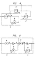
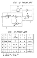
- FIG. 12 shows a conventional master/slave latch circuit belonging to the prior art.
- an input A to a master latch circuit M An input B to a slave latch circuit S is the output of the master latch circuit M. Also shown are an output C of the slave latch circuit S and a control signal ⁇ .
- a master input gate G s and a slave latching gate G 8 have enable state and disable states controlled by a control signal ⁇ and have respective outputs O 5 and O 6 .
- a master latching gate G 6 and a slave input gate G have their enable states and disable states controlled by a control signal - ⁇ and have respective outputs 0, and O 8 .
- the control signal - ⁇ is the complement of the control signal ⁇ .
- the master latch circuit M contains a buffer B3 and in the slave latch circuit S contains a buffer B 4 .
- Figure 13 is a table indicating the states of the gates G s through G 6 and of the latch circuit outputs B and C with the states of the control signal ⁇ .
- the gates G6 and G7 are disabled.
- the signal of the input A is applied to the output O 5 of the gate G s .
- the slave latch circuit S the signal of the output C existing before the change of the control signal ⁇ is latched by the gate G 8 and the buffer B 4 .
- the gates G s and G 8 are disabled while the gates G6 and G 7 are placed in an enabled state.
- the master latch circuit M the signal of the output B existing before the control signal ⁇ is inverted is latched by the gate G 6 and the buffer B 3 .
- the signal of the output B latched by the master latch circuit M is transmitted through the gate G 7 in the slave latch circuit S and thus transmitted to the output C.
- the conventional master/slave latch circuit suffers from a difficulty that, when the potential of the control signal ⁇ becomes unstable between the "H (high)” potential and the "L (low)” potential (for instance the potential of the control signal ⁇ changes slowly from “L” to "H"), the signal of the input A read into the master latch circuit M is directly transmitted to the output C of the slave latch circuit S.
- the signal provided at the output B (described later) is determined by which one of the outputs of the master input gate G s and the slave latching gate G, has the smaller output impedance.
- the signal provided at the output C is determined by which one of the outputs of the master latching gate G 6 and the slave input gate G7 has the smaller output impedance.
- the input gate G s in the master latch circuit and the input gate G 7 in the slave latch circuit are made large in transistor size.
- the master latching gate G 6 and the slave latching gate G 8 are made small in transistor size. Accordingly, in the above-described case, when the potential of the control signal ⁇ is ⁇ 3 (O ⁇ ⁇ 3 ⁇ ⁇ 0 ), then the output impedance Z s of the master input gate G s becomes equal to the output impedance Z, of the master latching gate G 6 .
- the output impedance Z 7 of the slave input gate G7 becomes equal to the output impedance Z 8 of the slave latching gate G 8 . Therefore, when ⁇ 3 ⁇ ⁇ ⁇ ⁇ 4 , the output impedance Z 5 of the master input gate G s is lower than the output impedance Z 6 of the master latching gate G., and the output impedance Z7 of the slave input gate G 7 is lower than the output impedance Z 8 of the slave latching gate G 8 .
- the output B the output 05 of the master input gate G s is provided as a "master” output while the output O 6 of the master latching gate G 6 is provided as a “slave” output.
- the output C the output 07 of the gate slave input G7 is provided as a "master” output while the output O s of the slave latching gate G 8 is provided as a “slave” output. That is, both of the outputs O s and 0, from the input gates G s and G 7 are provided as "master " outputs, and the signal of the input A read into the master latch circuit M is transmitted directly to the slave latch circuit output C with the result that the function of the master/slave latch circuit is not correctly performed. That is, the master/slave latch circuit operates erroneously.
- the object of this invention is to eliminate the above-described difficulties accompanying a conventional master/slave latch circuit.
- an object of the invention is to provide a master/slave latch circuit in which its original master/slave latch function is correctly per- ormed and the erroneous operation is prevented.
- a master/slave latch circuit is so designed that, irrespective of the magnitude of voltage of a gate control signal, the output of a reading gate in the master latch circuit and the output of a reading gate in the slave latch circuit are not provided as "master" outputs simultaneously.
- the master/slave latch of the invention there is provided a means for preventing, irrespective of the value of voltage of the gate control signal, the simultaneous output of the input gate in the master latch circuit and the output of the input gate in the slave latch circuit. Thus, the outputting of the input signal of the master latch circuit directly from the slave latch circuit is prevented.
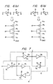
- FIG. 1 A first embodiment of this invention will be described with reference to Fig. 1.
- the outward form of this circuit is the same as that of Fig. 12, although the elements have been renumbered. Most importantly, the output impedances of the gates are restricted.
- Fig. 2 indicates the states of outputs 0, through 0, of gates G, through G 4 and the latch circuit outputs B and C as a function of the voltages of the control signal ⁇ .
- reference characters Z, through Z 4 designate respectively the output impedances of the master input gate G,, the master latching gate G 2 , the slave input gate G, and the slave latching gate G 4 .
- Z is equal to or greater than Z 2 and Z 3 is greater than Z 4 and these output impedances are selected from the range of 100 ohms to 1,000 ohms so as to meet the characteristics of transistors used therein.
- B, and B2 respectively represent the buffers in the master latch circuit and the slave latch circuit.
- the enabled and disabled states of the gates G, and G. are controlled by the control signal ⁇ while the enabled and disabled states of the gates G2 and G 3 are controlled by the complemented control signal - ⁇ .
- the gates G, and G 4 are in the enabled state and the gate G2 and G, are in the disabled state, in the master latch circuit the signal of the input A is transmitted to the output 0, of the master input gate G, while in the slave latch circuit the signal of the output C provided before the change of the control signal ⁇ is latched by the slave latching gate G4 and the buffer B2.
- the gates G, and G 4 are disabled while the gates G 2 and G 3 are enabled.
- the signal of the output B provided before inversion of the control signal ⁇ is latched by the master latching gate G2 and the buffer B,, while in the slave latch circuit the signal of the output B thus latched is read by the slave input gate G 3 and transmitted to the output C.
- the output impedance Z 2 of the latching gate G 2 is less than output the impedance Z, of the input gate G,. Therefore, at the master output B, the potential of the output O 2 of the master latching gate G 2 is provided as a "master” potential while the potential of the output O, of the master input gate G, is provided as a "slave” potential (cf. the parts (a) and (b) of Fig. 3). In the slave latch circuit, the output impedance Z4 of the latching gate G 4 is less than the output impedance Z 3 of the input gate G 3 .
- the potential of the output O 4 of the slave latching gate G is provided as a "master” potential while the potential of the output O 3 of the slave input gate G, is provided as a "slave” potential (cf. parts (c) and - (d) of Fig. 3).
- the output impedance Z, of the slave input gate G 3 becomes equal to the output impedance Z 4 of the slave latching gate G 4 .
- the output impedance Z, of the master input gate G becomes equal to the output impedance Z 2 of the master input gate G 2 .
- the output B when 0 ⁇ ⁇ ⁇ ⁇ 2 , the output O 2 of the master latching gate G 2 is provided as a "master” output while the output O 1 of the gate G, is provided as a “slave” output. Also, when ⁇ 2 ⁇ ⁇ ⁇ Vcc, the output O, of the master input gate G, is provided provided as a "master” output while the output O 2 of the master latching gate G 2 is provided as a "slave” output. And at the output C, when 0 ⁇ ⁇ ⁇ ⁇ 1 , the output 0, of the slave input gate G3 is provided as a "master” output while the output O 4 of the slave latching gate G 4 is provided as a "slave” output.
- the buffers B, and B2 are employed.
- a circuit as shown in Fig. 4 in which the buffers B, and B 2 are not employed may be used with the same effect as the above-described embodiment.
- the output B of the master latch circuit is the connecting point of the output O, of the master input gate G, and the output O 2 of the master latching gate G2.
- the output C of the slave latch circuit S is the connecting point of the output O 3 of the slave input gate G 3 and the output O 4 of the slave latching gate G 4 .
- the circuit may be so modified that, as shown in Fig. 5, the input of the master latching gate G2 is the output B of the master latch circuit M, and the input of the slave latching gate G 4 is the output C of the slave latch circuit S.
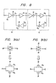
- the first embodiment has been described with reference to the ordinary master/slave latch circuit. However, it may be modified as follows.
- the gates are replaced by clocked gates as shown in Figs. 6-(a) and 6(b) to form a circuit as shown in Fig. 7 or 8, and the output impedance Z, through Z 4 of the clocked gates G, through G 4 are determined similarly as in the case of the above-described embodiment.
- the modification can provide the same effect as the above-described embodiment.
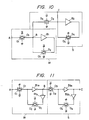
- transmission gates as shown in the Figs. 9(a) and 9(b) may be employed to form a circuit as shown in Fig. 10 or 11, and the output impedance Z, through Z 4 of the transmission gates G, through G 4 are determined similarly as in the case of the above-described embodiment.
- This modification also can provide the same effect as the above-described embodiment.
- reference characters P, through P 6 designate P-channel MOS transistors, and N through N 6 N-channel MOS transistors.
- the master/slave latch circuit according to the invention is so designed that, when the voltage of the control signal ⁇ or - ⁇ changes slowly in the range of 0V to V cc , the output of the reading gate in the master latch circuit and the output of the reading gate in the slave latch circuit may not be provided as "master" outputs simultaneously. Therefore, the master/slave latch circuit of the invention is free from the erroneous operation that the signal of the input A is transmitted through the output B of the master latch circuit directly to the slave latch circuit output C.
Landscapes
- Engineering & Computer Science (AREA)
- Microelectronics & Electronic Packaging (AREA)
- Computer Hardware Design (AREA)
- Logic Circuits (AREA)
- Static Random-Access Memory (AREA)
Applications Claiming Priority (3)
| Application Number | Priority Date | Filing Date | Title |
|---|---|---|---|
| JP60235715A JPS6295016A (ja) | 1985-10-21 | 1985-10-21 | ラツチ回路 |
| JP235715/85 | 1985-10-21 | ||
| JP23571585 | 1985-10-21 |
Publications (3)
| Publication Number | Publication Date |
|---|---|
| EP0219846A2 true EP0219846A2 (de) | 1987-04-29 |
| EP0219846A3 EP0219846A3 (de) | 1989-09-06 |
| EP0219846B1 EP0219846B1 (de) | 2000-05-24 |
Family
ID=16990152
Family Applications (1)
| Application Number | Title | Priority Date | Filing Date |
|---|---|---|---|
| EP86114529A Expired - Lifetime EP0219846B1 (de) | 1985-10-21 | 1986-10-21 | Gegenüber undefinierten Steuersignalen tolerante Verriegelungsschaltung |
Country Status (5)
| Country | Link |
|---|---|
| US (1) | US4794276A (de) |
| EP (1) | EP0219846B1 (de) |
| JP (1) | JPS6295016A (de) |
| KR (1) | KR900001777B1 (de) |
| DE (1) | DE3650746T2 (de) |
Cited By (7)
| Publication number | Priority date | Publication date | Assignee | Title |
|---|---|---|---|---|
| EP0308294A3 (de) * | 1987-09-18 | 1991-04-03 | STMicroelectronics, Inc. | Geräuschbeständige Arbitrierungsschaltung |
| EP0416576A3 (en) * | 1989-09-05 | 1992-04-01 | Kabushiki Kaisha Toshiba | Flip-flop circuit |
| EP0472426A3 (en) * | 1990-08-24 | 1992-05-13 | Ncr Corporation | Cmos flip-flop circuit |
| EP0516230A3 (en) * | 1991-05-31 | 1993-04-28 | Koninkl Philips Electronics Nv | Electronic flip-flop circuit, and integrated circuit comprising the flip-flop circuit |
| WO1993019529A1 (en) * | 1992-03-19 | 1993-09-30 | Vlsi Technology Inc. | Asynchronous-to-synchronous synchronizers, particularly cmos synchronizers |
| EP0317901B1 (de) * | 1987-11-24 | 1994-05-18 | National Semiconductor Corporation | Synchronisierer mit endlicher metastabiler Dauer |
| FR2802733A1 (fr) * | 1999-12-21 | 2001-06-22 | St Microelectronics Sa | Bascule de type d maitre-esclave securisee |
Families Citing this family (9)
| Publication number | Priority date | Publication date | Assignee | Title |
|---|---|---|---|---|
| JP2562995B2 (ja) * | 1990-11-27 | 1996-12-11 | 三菱電機株式会社 | データ処理回路の制御方法 |
| JPH04263510A (ja) * | 1991-02-18 | 1992-09-18 | Nec Corp | フリップフロップ回路 |
| JP2903990B2 (ja) * | 1994-02-28 | 1999-06-14 | 日本電気株式会社 | 走査回路 |
| TW281726B (de) * | 1994-07-05 | 1996-07-21 | Philips Electronics Nv | |
| EP0713292A3 (de) * | 1994-11-21 | 1997-10-01 | Motorola Inc | Rückgekoppelte Verriegelungsschaltung und deren Betriebsverfahren |
| US5789956A (en) * | 1995-05-26 | 1998-08-04 | Texas Instruments Incorporated | Low power flip-flop |
| US20040150449A1 (en) * | 2003-01-30 | 2004-08-05 | Sun Microsystems, Inc. | High-speed flip-flop circuitry and method for operating the same |
| JP2005160088A (ja) * | 2003-11-27 | 2005-06-16 | Samsung Electronics Co Ltd | パルスベースフリップフロップ |
| US20080186070A1 (en) * | 2006-04-27 | 2008-08-07 | Arun Sundaresan Iyer | Higher operating frequency latch circuit |
Family Cites Families (10)
| Publication number | Priority date | Publication date | Assignee | Title |
|---|---|---|---|---|
| US3720848A (en) * | 1971-07-01 | 1973-03-13 | Motorola Inc | Solid-state relay |
| US4250406A (en) * | 1978-12-21 | 1981-02-10 | Motorola, Inc. | Single clock CMOS logic circuit with selected threshold voltages |
| JPS5685934A (en) * | 1979-12-14 | 1981-07-13 | Nippon Telegr & Teleph Corp <Ntt> | Control signal generating circuit |
| US4495629A (en) * | 1983-01-25 | 1985-01-22 | Storage Technology Partners | CMOS scannable latch |
| JPS59151537A (ja) * | 1983-01-29 | 1984-08-30 | Toshiba Corp | 相補mos形回路 |
| US4484087A (en) * | 1983-03-23 | 1984-11-20 | General Electric Company | CMOS latch cell including five transistors, and static flip-flops employing the cell |
| US4554467A (en) * | 1983-06-22 | 1985-11-19 | Motorola, Inc. | CMOS Flip-flop |
| DE3443798A1 (de) * | 1984-11-30 | 1986-06-12 | Siemens AG, 1000 Berlin und 8000 München | In c-mos-technik hergestellte, bistabile kippschaltung |
| FR2578125B1 (fr) * | 1985-02-28 | 1987-04-10 | Efcis | Bascule bistable statique en technologie cmos |
| JPS61263313A (ja) * | 1985-05-17 | 1986-11-21 | Matsushita Electric Ind Co Ltd | セレクタ付ラツチ回路 |
-
1985
- 1985-10-21 JP JP60235715A patent/JPS6295016A/ja active Granted
-
1986
- 1986-07-30 KR KR1019860006267A patent/KR900001777B1/ko not_active Expired
- 1986-10-21 EP EP86114529A patent/EP0219846B1/de not_active Expired - Lifetime
- 1986-10-21 DE DE3650746T patent/DE3650746T2/de not_active Expired - Lifetime
- 1986-10-21 US US06/921,180 patent/US4794276A/en not_active Expired - Lifetime
Cited By (10)
| Publication number | Priority date | Publication date | Assignee | Title |
|---|---|---|---|---|
| EP0308294A3 (de) * | 1987-09-18 | 1991-04-03 | STMicroelectronics, Inc. | Geräuschbeständige Arbitrierungsschaltung |
| EP0317901B1 (de) * | 1987-11-24 | 1994-05-18 | National Semiconductor Corporation | Synchronisierer mit endlicher metastabiler Dauer |
| EP0416576A3 (en) * | 1989-09-05 | 1992-04-01 | Kabushiki Kaisha Toshiba | Flip-flop circuit |
| EP0472426A3 (en) * | 1990-08-24 | 1992-05-13 | Ncr Corporation | Cmos flip-flop circuit |
| EP0516230A3 (en) * | 1991-05-31 | 1993-04-28 | Koninkl Philips Electronics Nv | Electronic flip-flop circuit, and integrated circuit comprising the flip-flop circuit |
| WO1993019529A1 (en) * | 1992-03-19 | 1993-09-30 | Vlsi Technology Inc. | Asynchronous-to-synchronous synchronizers, particularly cmos synchronizers |
| US5418407A (en) * | 1992-03-19 | 1995-05-23 | Vlsi Technology, Inc. | Asynchronous to synchronous particularly CMOS synchronizers |
| FR2802733A1 (fr) * | 1999-12-21 | 2001-06-22 | St Microelectronics Sa | Bascule de type d maitre-esclave securisee |
| EP1111783A1 (de) * | 1999-12-21 | 2001-06-27 | STMicroelectronics SA | Gesicherte Typ D Master-Slave Kippschaltung |
| US6424196B2 (en) | 1999-12-21 | 2002-07-23 | Stmicroelectronics S.A. | Secured master-slave D type flip-flop circuit |
Also Published As
| Publication number | Publication date |
|---|---|
| JPH0348689B2 (de) | 1991-07-25 |
| DE3650746D1 (de) | 2000-06-29 |
| DE3650746T2 (de) | 2000-10-19 |
| KR870004446A (ko) | 1987-05-09 |
| KR900001777B1 (ko) | 1990-03-24 |
| JPS6295016A (ja) | 1987-05-01 |
| EP0219846A3 (de) | 1989-09-06 |
| US4794276A (en) | 1988-12-27 |
| EP0219846B1 (de) | 2000-05-24 |
Similar Documents
| Publication | Publication Date | Title |
|---|---|---|
| EP0219846A2 (de) | Gegenüber undefinierten Steuersignalen tolerante Verriegelungsschaltung | |
| US7425844B1 (en) | Input buffer for multiple differential I/O standards | |
| US5144167A (en) | Zero power, high impedance TTL-to-CMOS converter | |
| US6911860B1 (en) | On/off reference voltage switch for multiple I/O standards | |
| US6285209B1 (en) | Interface circuit and input buffer integrated circuit including the same | |
| US5036226A (en) | Signal converting circuit | |
| US4763022A (en) | TTL-to-CMOS buffer | |
| US4101788A (en) | Mos buffer circuit | |
| US5663669A (en) | Circuitry and method for latching information | |
| US6084431A (en) | Output circuit providing protection against external voltages in excess of power-supply voltage | |
| EP0450453B1 (de) | BICMOS-Eingangsschaltkreis zur Erkennung von Signalen ausserhalb des ECL-Bereiches | |
| JPS63161720A (ja) | Cmos論理回路 | |
| US5530401A (en) | Single source differential circuit | |
| JPS6041325A (ja) | 半導体集積回路 | |
| EP1360765A2 (de) | Puffer mit reduzierten eingangs/ausgangspannungen | |
| US4687955A (en) | Schmitt circuit with MIS field effect transistors | |
| KR100190212B1 (ko) | 신호선 절환 회로 | |
| JPS63302622A (ja) | インタフエ−ス回路 | |
| JP2735268B2 (ja) | Lsiの出力バッファ | |
| JPH0330327B2 (de) | ||
| JP2599396B2 (ja) | 排他的論理回路 | |
| KR950007514Y1 (ko) | 반도체 장치의 출력 포트회로 | |
| JPS62297916A (ja) | デ−タ入力回路 | |
| KR100192583B1 (ko) | 출력버퍼회로 | |
| JPH02123821A (ja) | 半導体回路 |
Legal Events
| Date | Code | Title | Description |
|---|---|---|---|
| PUAI | Public reference made under article 153(3) epc to a published international application that has entered the european phase |
Free format text: ORIGINAL CODE: 0009012 |
|
| AK | Designated contracting states |
Kind code of ref document: A2 Designated state(s): DE GB NL |
|
| PUAL | Search report despatched |
Free format text: ORIGINAL CODE: 0009013 |
|
| AK | Designated contracting states |
Kind code of ref document: A3 Designated state(s): DE GB NL |
|
| RAP1 | Party data changed (applicant data changed or rights of an application transferred) |
Owner name: MITSUBISHI DENKI KABUSHIKI KAISHA |
|
| RIN1 | Information on inventor provided before grant (corrected) |
Inventor name: OKITAKA, TAKENORI MITSUBISHI DENKI K.K. Inventor name: SASADA, TATSUYOSHI MITSUBISHI DENKI K.K. |
|
| 17P | Request for examination filed |
Effective date: 19891120 |
|
| 17Q | First examination report despatched |
Effective date: 19900511 |
|
| APAB | Appeal dossier modified |
Free format text: ORIGINAL CODE: EPIDOS NOAPE |
|
| GRAG | Despatch of communication of intention to grant |
Free format text: ORIGINAL CODE: EPIDOS AGRA |
|
| GRAH | Despatch of communication of intention to grant a patent |
Free format text: ORIGINAL CODE: EPIDOS IGRA |
|
| 17Q | First examination report despatched |
Effective date: 19900511 |
|
| GRAH | Despatch of communication of intention to grant a patent |
Free format text: ORIGINAL CODE: EPIDOS IGRA |
|
| GRAA | (expected) grant |
Free format text: ORIGINAL CODE: 0009210 |
|
| AK | Designated contracting states |
Kind code of ref document: B1 Designated state(s): DE GB NL |
|
| REF | Corresponds to: |
Ref document number: 3650746 Country of ref document: DE Date of ref document: 20000629 |
|
| EN | Fr: translation not filed | ||
| PLBE | No opposition filed within time limit |
Free format text: ORIGINAL CODE: 0009261 |
|
| STAA | Information on the status of an ep patent application or granted ep patent |
Free format text: STATUS: NO OPPOSITION FILED WITHIN TIME LIMIT |
|
| 26N | No opposition filed | ||
| REG | Reference to a national code |
Ref country code: GB Ref legal event code: IF02 |
|
| APAH | Appeal reference modified |
Free format text: ORIGINAL CODE: EPIDOSCREFNO |
|
| PGFP | Annual fee paid to national office [announced via postgrant information from national office to epo] |
Ref country code: DE Payment date: 20051014 Year of fee payment: 20 |
|
| PGFP | Annual fee paid to national office [announced via postgrant information from national office to epo] |
Ref country code: NL Payment date: 20051016 Year of fee payment: 20 |
|
| PGFP | Annual fee paid to national office [announced via postgrant information from national office to epo] |
Ref country code: GB Payment date: 20051019 Year of fee payment: 20 |
|
| PG25 | Lapsed in a contracting state [announced via postgrant information from national office to epo] |
Ref country code: GB Free format text: LAPSE BECAUSE OF EXPIRATION OF PROTECTION Effective date: 20061020 |
|
| PG25 | Lapsed in a contracting state [announced via postgrant information from national office to epo] |
Ref country code: NL Free format text: LAPSE BECAUSE OF EXPIRATION OF PROTECTION Effective date: 20061021 |
|
| REG | Reference to a national code |
Ref country code: GB Ref legal event code: PE20 |
|
| NLV7 | Nl: ceased due to reaching the maximum lifetime of a patent |
Effective date: 20061021 |