EP0209113B1 - Structures redondantes de conducteurs pour dispositifs d'affichage à cristal liquide, commandés par des transistors à effet de champ en couche mince - Google Patents
Structures redondantes de conducteurs pour dispositifs d'affichage à cristal liquide, commandés par des transistors à effet de champ en couche mince Download PDFInfo
- Publication number
- EP0209113B1 EP0209113B1 EP86109677A EP86109677A EP0209113B1 EP 0209113 B1 EP0209113 B1 EP 0209113B1 EP 86109677 A EP86109677 A EP 86109677A EP 86109677 A EP86109677 A EP 86109677A EP 0209113 B1 EP0209113 B1 EP 0209113B1
- Authority
- EP
- European Patent Office
- Prior art keywords
- layer
- gate
- display
- data lines
- lines
- Prior art date
- Legal status (The legal status is an assumption and is not a legal conclusion. Google has not performed a legal analysis and makes no representation as to the accuracy of the status listed.)
- Expired - Lifetime
Links
Images


Classifications
-
- G—PHYSICS
- G02—OPTICS
- G02F—OPTICAL DEVICES OR ARRANGEMENTS FOR THE CONTROL OF LIGHT BY MODIFICATION OF THE OPTICAL PROPERTIES OF THE MEDIA OF THE ELEMENTS INVOLVED THEREIN; NON-LINEAR OPTICS; FREQUENCY-CHANGING OF LIGHT; OPTICAL LOGIC ELEMENTS; OPTICAL ANALOGUE/DIGITAL CONVERTERS
- G02F1/00—Devices or arrangements for the control of the intensity, colour, phase, polarisation or direction of light arriving from an independent light source, e.g. switching, gating or modulating; Non-linear optics
- G02F1/01—Devices or arrangements for the control of the intensity, colour, phase, polarisation or direction of light arriving from an independent light source, e.g. switching, gating or modulating; Non-linear optics for the control of the intensity, phase, polarisation or colour
- G02F1/13—Devices or arrangements for the control of the intensity, colour, phase, polarisation or direction of light arriving from an independent light source, e.g. switching, gating or modulating; Non-linear optics for the control of the intensity, phase, polarisation or colour based on liquid crystals, e.g. single liquid crystal display cells
- G02F1/133—Constructional arrangements; Operation of liquid crystal cells; Circuit arrangements
- G02F1/136—Liquid crystal cells structurally associated with a semi-conducting layer or substrate, e.g. cells forming part of an integrated circuit
- G02F1/1362—Active matrix addressed cells
- G02F1/1368—Active matrix addressed cells in which the switching element is a three-electrode device
-
- G—PHYSICS
- G02—OPTICS
- G02F—OPTICAL DEVICES OR ARRANGEMENTS FOR THE CONTROL OF LIGHT BY MODIFICATION OF THE OPTICAL PROPERTIES OF THE MEDIA OF THE ELEMENTS INVOLVED THEREIN; NON-LINEAR OPTICS; FREQUENCY-CHANGING OF LIGHT; OPTICAL LOGIC ELEMENTS; OPTICAL ANALOGUE/DIGITAL CONVERTERS
- G02F1/00—Devices or arrangements for the control of the intensity, colour, phase, polarisation or direction of light arriving from an independent light source, e.g. switching, gating or modulating; Non-linear optics
- G02F1/01—Devices or arrangements for the control of the intensity, colour, phase, polarisation or direction of light arriving from an independent light source, e.g. switching, gating or modulating; Non-linear optics for the control of the intensity, phase, polarisation or colour
- G02F1/13—Devices or arrangements for the control of the intensity, colour, phase, polarisation or direction of light arriving from an independent light source, e.g. switching, gating or modulating; Non-linear optics for the control of the intensity, phase, polarisation or colour based on liquid crystals, e.g. single liquid crystal display cells
- G02F1/133—Constructional arrangements; Operation of liquid crystal cells; Circuit arrangements
- G02F1/1333—Constructional arrangements; Manufacturing methods
- G02F1/1335—Structural association of cells with optical devices, e.g. polarisers or reflectors
- G02F1/133509—Filters, e.g. light shielding masks
- G02F1/133512—Light shielding layers, e.g. black matrix
-
- G—PHYSICS
- G02—OPTICS
- G02F—OPTICAL DEVICES OR ARRANGEMENTS FOR THE CONTROL OF LIGHT BY MODIFICATION OF THE OPTICAL PROPERTIES OF THE MEDIA OF THE ELEMENTS INVOLVED THEREIN; NON-LINEAR OPTICS; FREQUENCY-CHANGING OF LIGHT; OPTICAL LOGIC ELEMENTS; OPTICAL ANALOGUE/DIGITAL CONVERTERS
- G02F1/00—Devices or arrangements for the control of the intensity, colour, phase, polarisation or direction of light arriving from an independent light source, e.g. switching, gating or modulating; Non-linear optics
- G02F1/01—Devices or arrangements for the control of the intensity, colour, phase, polarisation or direction of light arriving from an independent light source, e.g. switching, gating or modulating; Non-linear optics for the control of the intensity, phase, polarisation or colour
- G02F1/13—Devices or arrangements for the control of the intensity, colour, phase, polarisation or direction of light arriving from an independent light source, e.g. switching, gating or modulating; Non-linear optics for the control of the intensity, phase, polarisation or colour based on liquid crystals, e.g. single liquid crystal display cells
- G02F1/133—Constructional arrangements; Operation of liquid crystal cells; Circuit arrangements
- G02F1/136—Liquid crystal cells structurally associated with a semi-conducting layer or substrate, e.g. cells forming part of an integrated circuit
- G02F1/1362—Active matrix addressed cells
- G02F1/136286—Wiring, e.g. gate line, drain line
- G02F1/13629—Multilayer wirings
-
- G—PHYSICS
- G02—OPTICS
- G02F—OPTICAL DEVICES OR ARRANGEMENTS FOR THE CONTROL OF LIGHT BY MODIFICATION OF THE OPTICAL PROPERTIES OF THE MEDIA OF THE ELEMENTS INVOLVED THEREIN; NON-LINEAR OPTICS; FREQUENCY-CHANGING OF LIGHT; OPTICAL LOGIC ELEMENTS; OPTICAL ANALOGUE/DIGITAL CONVERTERS
- G02F2202/00—Materials and properties
- G02F2202/10—Materials and properties semiconductor
- G02F2202/103—Materials and properties semiconductor a-Si
Definitions
- the present invention is generally directed to the construction of liquid crystal display devices. More particularly, the present invention is directed to redundant conductor structures provided for x and y address lines in liquid crystal display (LCD) devices.
- LCD liquid crystal display
- a liquid crystal display device typically comprises a pair of flat panels sealably containing a quantity of liquid crystal material. These liquid crystal materials typically fall into two categories: dichroic dyes in a guest/host system or twisted nematic materials.
- the flat panels generally possess transparent electrode material disposed on their inner surfaces in predetermined patterns. One panel is often covered completely by a single transparent "ground plane” electrode. The opposite panel is configured with an array of transparent electrodes, referred to herein as "pixel" (picture element) electrodes.
- pixel picture element
- the typical cell in a liquid crystal display includes liquid crystal material disposed between a pixel electrode and a ground electrode forming, in effect, a capacitor-like structure disposed between transparent front and back panels. In general, however, transparency is only required for one of the two panels and the electrodes disposed thereon.
- the orientation of liquid crystal material is affected by voltages applied across the electrodes on either side of the liquid crystal material.
- a voltage applied to the pixel electrode effects a change in the optical properties of the liquid crystal material.
- This optical change causes the display of information on the liquid crystal display (LCD) screen.
- LCD liquid crystal display
- the visual effect is typically produced by variations in reflected light.
- the utilization of transparent front and back panels and transparent electrodes also permit the visual effects to be produced by transmissive effects. These transmissive effects may be facilitated by separately powered light sources for the display, including fluorescent light type devices.
- LCD display screens may also be employed to produce color images through the incorporation of color filter mosaics in registration with the pixel electrode array. Some of these structures may employ polarizing filters to either enhance or provide the desired visual effect.
- CMOS complementary metal oxide varistor devices
- FET thin film field effect transistor
- the pixel elements in an LCD are typically arranged in a rectangular array of rows and columns. Each pixel electrode is associated with its own FET switch device. Each switch device is connected to a data line and a gate line. Electrical signals applied simultaneously to each of these lines permit each pixel to be addressed independently. Accordingly, the LCD is typically provided with a set of parallel data lines which can be made to address cells in a horizontal or x direction. Likewise, gate lines are provided for accessing cells in a vertical or y direction. In operation, the image on the LCD device may be refreshed at a rate which is typically approximately 60 Hz.
- amorphous silicon FET addressed liquid crystal matrix displays provide an attractive approach to high contrast, flat panel television type displays.
- the FET addressed LCD device when the FET is turned on, the "liquid crystal capacitor” charges to the data or source line voltage. When the FET is turned off, the data voltage is stored on the liquid crystal capacitor.
- the horizontal and vertical address lines (that is, the gate lines and data lines) must all be continuous.
- the total length of the address lines is approximately 100,000 mm.
- the width of the lines should be less than approximately 10 ⁇ m in order to maintain a high relative percentage of active cell area in the display. In the fabrication of these devices, defects can occur in many of the processing steps.
- defects in these lines may occur as a result of dust or dirt interfering with metal deposition or adhesion, flaws in photoresist patterns used to etch the metal lines, scratches, etc. Additionally, defects in these lines can result from unsatisfactory step coverage. This occurs in those situations where metal lines are required to traverse a vertical or near vertical side wall structure, for example, in an etched insulating later. These steps typically occur at points in the device at which the horizontal and vertical lines cross over one another. In integrated circuit fabrication, typical open line defect probabilities for lines of this width are of the order of 10 ⁇ 5 per mm. It is therefore apparent that methods for reducing the probability of open x and y addressing lines and methods for enhancing the yield of the LCD device are desired.
- a liquid crystal display according to the invention is defined in claim 1.
- Another such display according to the invention is defined in claim 19.
- a liquid crystal display comprises a pair of flat substrates with at least one of them being transparent.
- a quantity of liquid crystal material is disposed and contained between the substrates.
- An array of pixel electrodes is disposed on at least one of the substrates.
- At least one ground plane electrode is disposed on the other of the substrates so that liquid crystal material is disposed between the pixel electrodes and any ground plane electrodes.
- Either the array of pixel electrodes comprise transparent material or the ground plane electrode or electrodes comprise transparent material.
- both substrates, the ground plane electrode, and the array of pixel electrodes comprise transparent conductive material such as indium tin oxide (ITO).
- An array of semiconductor switch elements is associated with each pixel electrode.
- a set of electrically conductive data lines and a set of electrically conductive gate lines are provided and configured with the switch elements so that voltages appearing on the data line are applied to select pixel electrodes.
- the semiconductor switch elements preferably comprise thin film field effect transistors.
- the data lines exhibit a multilayer structure extending for at least a portion of their length with at least two of these layers comprising conductive material in electrical contact along a portion of their length. This structure provides redundancy of up to 90% along the data line length.
- the data lines comprise a three layer structure with the intermediate layer comprising the same insulating material as the gate insulation for the FET.
- the first layer of data line metal is preferably deposited at the same time as the gate metal. Accordingly, this metal pattern is incorporated in the gate metal mask pattern.
- the second or upper conductive layer comprises metal deposited at the same time as the source and drain metal for the FET switches.
- the presence of the insulating layer and its configuration permit the upper data line layer to be applied without steep step crossovers at the gate line intersections. Electrical contact is established between the conductive layers in the data lines on either side of a narrower strip in the insulating layer. While contact is made along a step structure, the length of this step is much longer, thereby insuring contact at least somewhere along its length. In this way, a redundant data line structure is provided. Similarly, in a preferred embodiment of the present invention, redundancy in the gate line layer is also provided. However, in this situation, it is not necessary to employ an intermediary insulating layer. It is also noted that the roles of the data lines and gate lines may be reversed by varying electrical connections with the switch element.
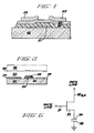
- FIG. 1 illustrates, in cross section, a conventional thin film FET used in LCD devices.
- substrate 20 typically comprises a transparent material such as glass.
- metal gate electrode 21 is affixed to this substrate.
- a patterned layer of insulating material 24 such as silicon nitride is then typically deposited so as to cover gate electrode 21 and to extend a certain distance on either side thereof.
- An active layer of amorphous silicon ( ⁇ -silicon) is then typically applied and doped with appropriate polarity dopants to produce a channel region wherein current flow is controlled by electrical signals applied to the gate electrode.
- source and drain electrodes 22 and 23, respectively, are deposited using photopatterning methods to complete the formation of a thin film FET device.
- gate material 21 is not a significant viewing limitation since the gate electrode may only be approximately 10 ⁇ m in width and therefore essentially invisible to the user.
- the pixel electrodes are by far the larger elements in an LCD device cell.
- the pixel electrodes are typically approximately 0.01 inches square (6,46 mm2).
- Figure 2 is particularly relevant to understanding the present invention.
- Figure 2 is a cross sectional view of a portion of Figure 5 which is more particularly described below.
- the upper portion of Figure 2 is shown in phantom view since these structures are, strictly speaking, not produced by the mask patterns in Figures 3A-3D.
- These mask patterns are typically employed to generate only one side of the substrates or panels which form major constituents in an LCD device.
- substrates 20 and 30 may typically comprise transparent material.
- ground plane 38 and pixel electrodes 39 are disposed on substrates 30 and 20, respectively. These electrodes may comprise transparent conductive material.
- the data line structure which includes data lines 32 and insulating material 34.
- first, conductive layer and the third, conductive layer are in electrical contact along either side of narrow insulating strip 34.
- the first, conductive data line layer is preferably fabricated in the same process stage as the gate electrodes of the FET switching elements.
- the second, insulating layer 34 is preferably fabricated in the same process stage as the gate insulating material.
- the third, conductive layer in the data line structure is preferably fabricated in the same process stage as the fabrication of the source and drain metallization. The presence of insulating layer 34 permits the third or upper conductive data line layer to cross gate lines, from which it is insulated, without the formation of step discontinuities which tend to decrease circuit reliability.
- first or lowermost conductive line is in contact with the upper conductive line and provides redundant circuit connection along approximately 90% of the length of each data line.
- Lowermost data line 32 is, however, provided with gaps to accommodate passage of gate line conductors. While it appears that a longer step jump is now required for contact between the conductive layers in the data line, this is in fact not a problem since insulating material strip 34 in Figure 2 is relatively narrow and since electrical contact is now possible along the entire length of the lower data line conductor.
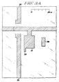
- Figures 3A-3D are layout patterns employable in the fabrication of the present invention.
- Figure 3A illustrates a pattern for gate metal and associated horizontal gate drive lines 31. A scale is provided for reference. Additionally, Figure 3A illustrates the presence of redundant data line 32. These lines are redundant in the sense that they do not form a complete electrical circuit in the layer shown but instead partially duplicate data line paths which are completed in whole in another layer as shown in Figure 3C. Nonetheless, connection is provided to complete the data line circuit, as shown in Figure 3C.
- the metallization layer shown in Figure 3A is preferably opaque so as to prevent light from reaching the channel regions from one side of the display. The channel regions are formed above the large rectangular area shown in Figure 3A.
- Metallic pad 36 is also shown in the layer illustrated in Figure 3A. Pad 36 facilitates electrical connection between the device drain and the pixel electrode.
- the pattern of Figure 3B is employed in the deposition of insulating and semiconducting layers.
- a layer of silicon nitride or other insulating material is deposited in the pattern shown in Figure 3B.
- the insulating material pattern shown in Figure 3B serves several purposes. Firstly, this pattern provides gate insulating material for thin film FET devices. Secondly, this insulating layer is disposed so as to electrically insulate the gate lines from the data lines. Lastly, it is noted that the vertical portions extending upwardly and downwardly from the central patch region of Figure 3B overlie data lines 32 shown in Figure 3A.
- the insulating layer in Figure 3B is narrower than data line 32 in Figure 3A. This permits the formation of a partially redundant data line as shown in Figure 3C. Because the width of insulating layer 34 in Figure 3B is narrower, electrical contact is thereby permitted between the data line conductors shown in Figures 3A and the complete data line conductors shown in Figure 3C, both of which are indicated by reference numeral 32.
- Figure 2 provides a cross sectional view of the resulting structure.
- the pattern of Figure 3B is employed to serve an additional function.
- it serves as a pattern for the deposition of a layer or layers of semiconductor material.
- it is preferable to employ a triple layer having the pattern shown in Figure 3B.
- the lowermost (that is, first) layer comprises silicon nitride
- the next layer comprises ⁇ -silicon
- the next layer comprises ⁇ -silicon doped with material so as to provide the layer with an N+ polarity.
- the next layer applied to the substrate is a metallization layer having the configuration illustrated in Figure 3C.
- the finger projections 32a and 32b extend from data line 32. These projections form source electrodes for an FET.
- Metallization pattern 33 provides a common drain electrode for the FET formed. This drain electrode is ultimately connected to pixel electrode 39 shown in Figures 2, 6, and 3D. It is also in electrical contact with pad 36 in Figure 3A.
- Data line 32 is connected to source electrodes 32a and 32b and in addition, because of the narrower width of insulating layer of Figure 3B, data line 32 is in contact with the partially redundant data line having the same reference numeral in the layer of Figure 3A. This provides a redundant structure for increased display reliability.
- gate line 31 is provided with enhanced metallization from the layer of Figure 3C, again to provide enhanced display reliability.
- the next layer to be applied is the layer of pixel electrode patterns.
- the pixel electrodes must necessarily comprise electrically conductive material. However, depending upon the specific nature of the LCD device, the electrically conductive material may or may not be transparent. However, for transparency, indium tin oxide is preferably employed for this purpose. Accordingly, although pixel electrodes 39 comprise electrically conductive material, they are hatched as glass in figures herein to suggest their potentially transparent nature. It is, of course, required that either the ground plane electrodes or the pixel electrodes, or both, comprise transparent material. If they are both opaque, the purpose of the display is defeated. With further reference to the pixel electrodes, it is noted that Figure 3D illustrates the presence of four such pixel electrodes. However, the semiconductor switch is in fact associated with the pixel electrode in the lower righthand corner of Figure 3D. This pixel electrode is in electrical contact with metal (drain) pad 33 in Figure 3C.
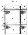
- Figure 4 illustrates in an enlarged view, a single pixel cell and portions of the cells which surround it.
- the gate lines associated with the cells are shown extending in a horizontal direction.
- the data lines associated with the cells are shown extending in a vertical direction. It is noted, however, that the relative directionality of these lines is not fixed and that alternate configurations may be employed in which the horizontal and vertical roles are reversed.
- each pixel cell is seen to be uniquely associated with a selected data line and gate line.
- Each pixel cell is seen to include a pixel electrode and its associated semiconductor switching device.
- the structure seen in Figure 4 typically comprises one side of a liquid crystal display device. The other side typically comprises a ground plane electrode disposed on a transparent substrate.
- Liquid crystal material is disposed between the pixel electrodes and the ground plane electrode or electrodes. While the pixel cells shown in Figure 4 are square, it is also possible to employ cells of differing shapes or varying sizes. Likewise, whale the data lines and gate lines are shown extending in horizontal and vertical directions, it is also possible to employ data lines disposed so as to more closely resemble oblique coordinate systems.
- Figure 5 provides a detailed view of the structure that results from the fabrication steps performed using the patterns shown in Figures 3A-3D.
- Figure 5 provides an overview of the resulting structure and serves to more particularly describe interlayer structural relationships.
- Figure 5 is also notable for the presence of section line 2 referring particularly to Figure 2 which show the cross section of a typical data line.
- Figure 6 provides an electrical schematic diagram for a single pixel cell.
- a capacitor symbol with upper plate 39 and lower plate 38 is employed to represent and suggest the capacitor portion of the cell.
- Lower plate 38 typically comprises the ground plane electrode and upper plate 39 typically comprises the individual pixel electrodes.
- the pixel electrodes are electrically connected to drains 33 of FET with gate 31 and source electrodes 32a and 32b.
- the gate lines and data lines are as shown in Figure 6. It should be noted, however, that references herein to source and drain electrodes are exemplary only. As is well known in the art, FET devices often exhibit symmetries in which source and drain designations exist only for convenience or as a result of external device connections.
- liquid crystal display devices which display color images rather than monochrome ones.
- a mosaic color filter is typically employed.
- This color filter is preferably disposed over the ground plane electrode.
- spacer material it is also possible to dispose spacer material on this filter. However, this is a less desirable arrangement for the reason that the color filter layer must be accurately registered and aligned with respect to the thin film transistor array and the associated pixel electrodes.
- liquid crystal material may be employed in the present invention.
- a pair of polarizers are also required. These polarizers are typically disposed external to the walls of the LCD device which contain the liquid crystal material. In LCD devices employing dichroic dyes (guest/host systems), polarizer pairs are no longer required. In these embodiments, systems with either a single polarizer or no polarizers at all may be employed.
- the liquid crystal display device of the present invention provides improved display performance, manufacturing yield and is compatible with conventionally employed LCD device fabrication methods. It is also seen that the present invention facilitates the formation of complete, high quality, high contrast images, even color images.
Claims (25)
- Un dispositif d'affichage à cristaux liquides comportant :- une paire de substrats (20, 30) plats dont l'un au moins (20) est transparent ;- une quantité de produit à cristaux liquides (50) placée et contenue entre lesdits substrats ;- un réseau d'électrodes de pixels (39) placé sur ledit au moins un substrat (20) ;- au moins une électrode plane (38) de terre placée sur l'autre desdits substrats, de telle sorte que le produit à cristaux liquides se trouve entre lesdites électrodes de pixels et l'une quelconque desdites électrodes planes de terre, avec l'une au moins desdites électrodes de terre et dudit réseau d'électrodes de pixels qui est transparente ;- un réseau d'éléments (21 à 25) formant commutateur à transistor à effet de champ en couche mince associé auxdites électrodes de pixels ;- un ensemble de lignes de données (32) électroconductrices ;- un ensemble de lignes de grilles (31) électroconductrices ;lesdits éléments formant commutateurs, lesdites lignes de données et lesdites lignes de grilles étant reliées électriquement pour appliquer les tensions qui apparaissent sur lesdites lignes de données à des électrodes de pixels choisies suivant les signaux présents sur lesdites lignes de grilles,
caractérisé en ce que,
composées de deux couches conductrices (32) séparées par une couche isolante (34), couches conductrices qui sont en contact électrique, lesdites lignes de données (32) ont une structure multicouches, laquelle s'étend sur au moins une partie de la longueur desdites grilles de données, lesdites lignes de grille (31) et lignes de données (32) sont isolées l'une de l'autre grâce à ladite couche isolante (34) qui se trouve dans lesdites lignes de données multicouches, ladite couche isolante s'étendant transversalement auxdites lignes de grilles de telle façon que lesdites lignes de données croisent lesdites lignes de grilles sans rencontrer de marche de discontinuité verticale substantielle. - Dispositif d'affichage de la revendication 1, dans lequel lesdits éléments formant commutateurs à transistor comportent des électrodes de source et de drain (32a, 32b, 33) dont une au moins (32a, 32b) montre des saillies multiples en forme de doigt.
- Dispositif d'affichage des revendications 1 et 2, dans lequel au moins deux desdites couches (32) desdites lignes de données consistent en un matériau conducteur en contact électrique sur une partie des longueurs desdites lignes de données.
- Dispositif d'affichage de l'une quelconque des revendications 1 à 3, dans lequel lesdits éléments formant commutateurs comportent une couche métallique de grille (21), une couche isolante de grille (24) et des motifs différents de source et de drain (22, 23) dans une couche métallique recouvrant ladite couche d'isolation de grille.
- Dispositif d'affichage des revendications 1 ou 4, dans lequel ladite structure multicouches comporte trois couches.
- Dispositif d'affichage de la revendication 5, dans lequel lesdites lignes de données comportent une première couche conductrice (32) coplanaire avec ledit métal de grille (31).
- Dispositif d'affichage de la revendication 6, dans lequel ladite première couche (32) de ligne de données comporte des trous par lesquels lesdites lignes de grille (31) passent.
- Dispositif d'affichage de la revendication 7, dans lequel lesdites lignes de données comportent une deuxième couche isolante (34) coplanaire avec ladite isolation de grille.
- Dispositif d'affichage de la revendication 8, dans lequel ladite seconde couche isolante s'étend transversalement auxdites lignes de grilles, grâce à quoi des lignes additionnelles conductrices des lignes de données croisent lesdites lignes de grille sans rencontrer de marche verticale.
- Dispositif d'affichage de la revendication 9, dans lequel lesdites lignes de données comportent une troisième couche conductrice (32), sensiblement continue, en contact avec ladite première couche conductrice (32).
- Dispositif d'affichage de la revendication 1, dans lequel lesdites lignes de données comportent une troisième couche (32) conductrice, sensiblement continue, placée sur ladite couche isolante (34).
- Dispositif d'affichage de la revendication 8, dans lequel lesdites lignes de données comportent une troisième couche (32) conductrice, sensiblement continue, coplanaire avec lesdits motifs métalliques de source et de drain.
- Dispositif d'affichage des revendications 1 ou 10, dans lequel ledit contact électrique se fait sur l'un ou l'autre côté de ladite couche isolante (34).
- Dispositif d'affichage de la revendication 1 ou 3, dans lequel lesdites lignes de grille comportent des première et deuxième couches conductrices.
- Dispositif d'affichage des revendications 4 ou 14, dans lequel lesdites lignes de grille sont constituées d'un matériau conducteur dans ladite première couche, coplanaire avec ledit métal de grille, et ledit matériau conducteur de la seconde couche est coplanaire avec lesdits motifs de source et de drain.
- Dispositif d'affichage de la revendication 15, dans lequel ladite seconde couche desdites lignes de grilles comporte des trous par lesquels passent lesdites lignes de données.
- Dispositif d'affichage de la revendication 15, dans lequel ladite première couche desdites lignes de grilles est sensiblement continue.
- Dispositif d'affichage de l'une quelconque des revendications 1 à 3, dans lequel éléments formant commutateur consistent en des transistors à effet de champ en silicium amorphe.
- Un dispositif d'affichage à cristaux liquides comportant :- une pluralité de cellules de pixels (38, 50, 39) arrangées sensiblement en colonnes et rangées ;- une pluralité de moyens formant éléments de commutation (21 à 25) pour mettre en position marche et arrêt les cellules individuelles de pixels ;- une pluralité de lignes de données (32) électroconductrices ; et- une pluralité de lignes de grilles (31) électroconductrices ;lesdits moyens formant éléments de commutation, lesdites lignes de données et lesdites lignes de grilles étant reliées électriquement pour permettre d'appliquer les tensions qui apparaissent sur lesdites lignes de données à des cellule de pixels choisies en fonction des signaux présents sur lesdites lignes de grilles, caractérisé en ce que,
chacun des moyens formant élément de commutation (21 à 25) comporte une structure d'électrodes entrecroisées (32a, 32b, 33) et chacun est couplé à un pixel différent de ladite pluralité de cellules de pixels,
et en ce que
chacune desdites lignes de données (32) a une structure multicouches (32, 34, 32) constituée de deux couches conductrices (32) séparées par une couche isolante (34), les deux couches conductrices étant en contact électrique. - Le dispositif d'affichage à cristaux liquides de la revendication 19, dans lequel chacun desdits moyens formant élément de commutation est un transistor à effet de champ en couche mince ayant au moins une couche (25) en matériau semi-conducteur.
- Le dispositif d'affichage à cristaux liquides de la revendication 20, dans lequel ladite au moins une couche (25) en matériau semi-conducteur est du silicium amorphe.
- Le dispositif d'affichage à cristaux liquides de la revendication 21, dans lequel chacun desdits transistors à effet de champ comporte :- une électrode de grille reliée à au moins une ligne de grille de ladite pluralité de lignes de grilles (31) ;- une électrode de source (32a, 32b) reliée à au moins une ligne de données de ladite pluralité de lignes de données (32) ; et- une électrode de drain (33) reliée à l'une des cellules de ladite pluralité de cellules de pixels (38, 39) ;au moins l'une de ladite électrode de source et ladite électrode de drain comportant une pluralité de saillies en forme de doigt (32a, 32a) placées de façon adjacente à au moins une saillie en forme de doigt (33) d'une autre desdites électrodes de source et de drain, de façon à former ladite structure d'électrodes entrecroisées.
- Un dispositif d'affichage à cristaux liquides de la revendication 19, dans lequel chacune desdites pluralités de lignes de données comporte :- une première couche (32) de matériau conducteur placée dans la même couche que lesdites lignes de grilles (31) avec des trous ;- une couche de matériau isolant (34) placée sur ladite première couche ; et- une seconde couche (32) de matériau conducteur placée sur ladite couche isolante et en contact avec ladite première couche conductrice le long d'au moins une partie de ladite ligne de données, chaque seconde couche de lignes de données s'étendant transversalement à chaque ligne de grilles et en étant séparée par ladite couche isolante, sans rencontrer de marche de discontinuité verticale substantielle.
- Le dispositif d'affichage à cristaux liquides de la revendication 19, dans lequel chacune desdites lignes de données (32) et desdites lignes de grilles (31) a une structure multicouches.
- Le dispositif d'affichage à cristaux liquides de la revendication 19, dans lequel chacune de ladite pluralité de lignes de grilles comporte :- une première couche de matériau conducteur ;- une couche de matériau isolant placée sur ladite première couche ; et- une deuxième couche de matériau conducteur placée sur ladite couche isolante et en contact avec ladite première couche conductrice le long d'au moins une partie de ladite ligne de grilles, chaque seconde couche conductrice de lignes de grilles comportant des trous par lesquels passent lesdites lignes de données.
Applications Claiming Priority (2)
| Application Number | Priority Date | Filing Date | Title |
|---|---|---|---|
| US75664085A | 1985-07-19 | 1985-07-19 | |
| US756640 | 1985-07-19 |
Publications (3)
| Publication Number | Publication Date |
|---|---|
| EP0209113A2 EP0209113A2 (fr) | 1987-01-21 |
| EP0209113A3 EP0209113A3 (en) | 1989-06-28 |
| EP0209113B1 true EP0209113B1 (fr) | 1993-01-13 |
Family
ID=25044403
Family Applications (1)
| Application Number | Title | Priority Date | Filing Date |
|---|---|---|---|
| EP86109677A Expired - Lifetime EP0209113B1 (fr) | 1985-07-19 | 1986-07-15 | Structures redondantes de conducteurs pour dispositifs d'affichage à cristal liquide, commandés par des transistors à effet de champ en couche mince |
Country Status (5)
| Country | Link |
|---|---|
| US (2) | US4804953A (fr) |
| EP (1) | EP0209113B1 (fr) |
| JP (1) | JPS6265017A (fr) |
| DE (1) | DE3687488T2 (fr) |
| FR (1) | FR2585167B1 (fr) |
Families Citing this family (71)
| Publication number | Priority date | Publication date | Assignee | Title |
|---|---|---|---|---|
| GB2169746B (en) * | 1984-11-13 | 1988-09-14 | Sharp Kk | Thin film transistor |
| DE3640174A1 (de) * | 1985-11-27 | 1987-06-04 | Sharp Kk | Duennfilm-transistor-anordnung |
| FR2593630B1 (fr) * | 1986-01-27 | 1988-03-18 | Maurice Francois | Ecran d'affichage a matrice active a resistance de drain et procedes de fabrication de cet ecran |
| US4762398A (en) * | 1987-01-26 | 1988-08-09 | Hosiden Electronics Co., Ltd. | Pixel transistor free of parasitic capacitance fluctuations from misalignment |
| US5270845A (en) * | 1987-02-19 | 1993-12-14 | Mitsubishi Denki K.K. | Liquid crystal display unit manufacturing method including forming one of two gate line layers of display electrode material |
| JPH0627985B2 (ja) * | 1987-05-06 | 1994-04-13 | 日本電気株式会社 | 薄膜トランジスタアレイ |
| JPH0690372B2 (ja) * | 1987-08-26 | 1994-11-14 | シャープ株式会社 | 液晶表示素子 |
| JPH01102434A (ja) * | 1987-10-15 | 1989-04-20 | Sharp Corp | マトリックス型液晶表示パネル |
| US5075674A (en) * | 1987-11-19 | 1991-12-24 | Sharp Kabushiki Kaisha | Active matrix substrate for liquid crystal display |
| JPH01191829A (ja) * | 1988-01-27 | 1989-08-01 | Mitsubishi Electric Corp | 液晶表示装置 |
| JPH0814668B2 (ja) * | 1988-02-16 | 1996-02-14 | シャープ株式会社 | マトリックス型液晶表示パネル |
| JPH01217421A (ja) * | 1988-02-26 | 1989-08-31 | Seikosha Co Ltd | 非晶質シリコン薄膜トランジスタアレイ基板およびその製造方法 |
| KR970008455B1 (en) * | 1988-03-18 | 1997-05-24 | Seiko Epson Corp | Thin film transistor |
| US5493129A (en) * | 1988-06-29 | 1996-02-20 | Hitachi, Ltd. | Thin film transistor structure having increased on-current |
| JPH02157828A (ja) * | 1988-12-12 | 1990-06-18 | Hosiden Electron Co Ltd | 液晶表示素子 |
| US4968119A (en) * | 1989-01-10 | 1990-11-06 | David Sarnoff Research Center, Inc. | High-density liquid-crystal active dot-matrix display structure |
| GB2227349A (en) * | 1989-01-18 | 1990-07-25 | Philips Electronic Associated | Display devices |
| US5153754A (en) * | 1989-06-30 | 1992-10-06 | General Electric Company | Multi-layer address lines for amorphous silicon liquid crystal display devices |
| US5212574A (en) * | 1989-07-05 | 1993-05-18 | Sharp Kabushiki Kaisha | Active matrix board having double-layer scan lines and capacity lines with discontinuous lower scan lines and lower capacity lines |
| AU6175190A (en) * | 1989-08-11 | 1991-03-11 | Raf Electronics Corp. | Wafer based active matrix |
| US5108172A (en) * | 1989-08-11 | 1992-04-28 | Raf Electronics Corp. | Active matrix reflective image plane module and projection system |
| US5498573A (en) * | 1989-11-29 | 1996-03-12 | General Electric Company | Method of making multi-layer address lines for amorphous silicon liquid crystal display devices |
| US5063378A (en) * | 1989-12-22 | 1991-11-05 | David Sarnoff Research Center, Inc. | Scanned liquid crystal display with select scanner redundancy |
| EP0717303B1 (fr) * | 1990-05-11 | 2003-05-02 | Sharp Kabushiki Kaisha | Dispositif d'affichage à matrice active, son procédé de fabrication et un procédé de traitement de pixels défectueux |
| US5162931A (en) * | 1990-11-06 | 1992-11-10 | Honeywell, Inc. | Method of manufacturing flat panel backplanes including redundant gate lines and displays made thereby |
| US5303074A (en) * | 1991-04-29 | 1994-04-12 | General Electric Company | Embedded repair lines for thin film electronic display or imager devices |
| US5302987A (en) * | 1991-05-15 | 1994-04-12 | Sharp Kabushiki Kaisha | Active matrix substrate including connecting electrode with extended portion |
| JPH055898A (ja) * | 1991-06-27 | 1993-01-14 | Casio Comput Co Ltd | 薄膜素子形成パネル |
| GB2265486A (en) * | 1992-03-11 | 1993-09-29 | Marconi Gec Ltd | Display device fabrication |
| JP2760462B2 (ja) * | 1992-05-13 | 1998-05-28 | シャープ株式会社 | アクティブマトリクス基板 |
| JP2915732B2 (ja) * | 1993-02-01 | 1999-07-05 | シャープ株式会社 | アクティブマトリクス基板 |
| JPH06250211A (ja) * | 1993-02-23 | 1994-09-09 | Hitachi Ltd | 液晶表示基板とその製造方法 |
| US5719065A (en) | 1993-10-01 | 1998-02-17 | Semiconductor Energy Laboratory Co., Ltd. | Method for manufacturing semiconductor device with removable spacers |
| WO1995017768A1 (fr) * | 1993-12-20 | 1995-06-29 | General Electronic Company | Procede et structure de reparation de ligne d'adresse pour dispositifs de formation d'images a couche mince. |
| US5555001A (en) * | 1994-03-08 | 1996-09-10 | Prime View Hk Limited | Redundant scheme for LCD display with integrated data driving circuit |
| US6943764B1 (en) | 1994-04-22 | 2005-09-13 | Semiconductor Energy Laboratory Co., Ltd. | Driver circuit for an active matrix display device |
| JP3402400B2 (ja) | 1994-04-22 | 2003-05-06 | 株式会社半導体エネルギー研究所 | 半導体集積回路の作製方法 |
| US5622163A (en) | 1994-11-29 | 1997-04-22 | Iep Group, Inc. | Counter for fluid dispensers |
| US5559345A (en) * | 1994-12-20 | 1996-09-24 | Goldstar Co., Ltd. | Thin film transistor having redundant metal patterns |
| US5814529A (en) * | 1995-01-17 | 1998-09-29 | Semiconductor Energy Laboratory Co., Ltd. | Method for producing a semiconductor integrated circuit including a thin film transistor and a capacitor |
| US5552607A (en) * | 1995-06-21 | 1996-09-03 | General Electric Company | Imager device with integral address line repair segments |
| US5631473A (en) * | 1995-06-21 | 1997-05-20 | General Electric Company | Solid state array with supplemental dielectric layer crossover structure |
| US6133977A (en) | 1997-10-21 | 2000-10-17 | Samsung Electronics Co., Ltd. | Liquid crystal displays having common electrode overlap with one or more data lines |
| US6215541B1 (en) | 1997-11-20 | 2001-04-10 | Samsung Electronics Co., Ltd. | Liquid crystal displays and manufacturing methods thereof |
| JP4674926B2 (ja) * | 1999-02-12 | 2011-04-20 | エーユー オプトロニクス コーポレイション | 液晶ディスプレイパネル及びその製造方法 |
| JP2000321599A (ja) * | 1999-05-10 | 2000-11-24 | Hitachi Ltd | 液晶表示装置 |
| KR100776514B1 (ko) * | 2000-12-30 | 2007-11-16 | 엘지.필립스 엘시디 주식회사 | 액정표시장치 및 그 제조방법 |
| US7038239B2 (en) | 2002-04-09 | 2006-05-02 | Semiconductor Energy Laboratory Co., Ltd. | Semiconductor element and display device using the same |
| JP3989761B2 (ja) | 2002-04-09 | 2007-10-10 | 株式会社半導体エネルギー研究所 | 半導体表示装置 |
| KR100968496B1 (ko) * | 2002-04-15 | 2010-07-07 | 가부시키가이샤 한도오따이 에네루기 켄큐쇼 | 표시장치 및 그 제조방법 |
| JP3989763B2 (ja) | 2002-04-15 | 2007-10-10 | 株式会社半導体エネルギー研究所 | 半導体表示装置 |
| JP2005524110A (ja) * | 2002-04-24 | 2005-08-11 | イー−インク コーポレイション | 電子表示装置 |
| US7256421B2 (en) | 2002-05-17 | 2007-08-14 | Semiconductor Energy Laboratory, Co., Ltd. | Display device having a structure for preventing the deterioration of a light emitting device |
| KR100862240B1 (ko) | 2002-07-31 | 2008-10-09 | 엘지디스플레이 주식회사 | 반사형 액정표시장치와 그 제조방법 |
| KR100460979B1 (ko) * | 2002-12-31 | 2004-12-09 | 엘지.필립스 엘시디 주식회사 | 반사형 액정표시장치용 어레이기판과 그 제조방법 |
| TWI226962B (en) | 2004-01-05 | 2005-01-21 | Au Optronics Corp | Liquid crystal display device with a capacitance-compensated structure |
| JP4275644B2 (ja) * | 2004-06-23 | 2009-06-10 | シャープ株式会社 | アクティブマトリクス基板およびその製造方法、並びに電子装置 |
| KR101138429B1 (ko) * | 2005-07-22 | 2012-04-26 | 삼성전자주식회사 | 박막 트랜지스터 기판 및 그 제조방법 |
| KR101232160B1 (ko) * | 2006-06-16 | 2013-02-12 | 엘지디스플레이 주식회사 | 표시장치와 그 제조방법 |
| CN100592181C (zh) * | 2007-05-30 | 2010-02-24 | 北京京东方光电科技有限公司 | 一种可修复的像素结构 |
| TWI501215B (zh) * | 2009-02-27 | 2015-09-21 | Au Optronics Corp | 減輕液晶顯示器拖曳殘影現象之方法及液晶顯示器 |
| WO2010141739A2 (fr) | 2009-06-03 | 2010-12-09 | Manufacturing Resources International Inc. | Rétroéclairage à del à gradation dynamique |
| CN102819158B (zh) * | 2012-08-10 | 2015-08-12 | 北京京东方光电科技有限公司 | 一种显示面板 |
| WO2014158642A1 (fr) | 2013-03-14 | 2014-10-02 | Manufacturing Resources International, Inc. | Ensemble d'affichage à cristaux liquides du type rigide |
| WO2015003130A1 (fr) | 2013-07-03 | 2015-01-08 | Manufacturing Resources International, Inc. | Ensemble de rétroéclairage de guide d'air |
| US10191212B2 (en) | 2013-12-02 | 2019-01-29 | Manufacturing Resources International, Inc. | Expandable light guide for backlight |
| US10527276B2 (en) | 2014-04-17 | 2020-01-07 | Manufacturing Resources International, Inc. | Rod as a lens element for light emitting diodes |
| US10649273B2 (en) | 2014-10-08 | 2020-05-12 | Manufacturing Resources International, Inc. | LED assembly for transparent liquid crystal display and static graphic |
| CN104505392A (zh) * | 2014-12-29 | 2015-04-08 | 合肥鑫晟光电科技有限公司 | 阵列基板及其制作方法、阵列基板的修复方法、显示装置 |
| US10261362B2 (en) | 2015-09-01 | 2019-04-16 | Manufacturing Resources International, Inc. | Optical sheet tensioner |
| CN107204375B (zh) * | 2017-05-19 | 2019-11-26 | 深圳市华星光电技术有限公司 | 薄膜晶体管及其制作方法 |
Family Cites Families (9)
| Publication number | Priority date | Publication date | Assignee | Title |
|---|---|---|---|---|
| US4368523A (en) * | 1979-12-20 | 1983-01-11 | Tokyo Shibaura Denki Kabushiki Kaisha | Liquid crystal display device having redundant pairs of address buses |
| GB2081018B (en) * | 1980-07-31 | 1985-06-26 | Suwa Seikosha Kk | Active matrix assembly for display device |
| DE3173506D1 (en) * | 1980-09-22 | 1986-02-27 | Toshiba Kk | Semiconductor device and its manufacture |
| JPS57161882A (en) * | 1981-03-31 | 1982-10-05 | Hitachi Ltd | Display body panel |
| JPS58140781A (ja) * | 1982-02-17 | 1983-08-20 | 株式会社日立製作所 | 画像表示装置 |
| JPS5997178A (ja) * | 1982-11-25 | 1984-06-04 | 三菱電機株式会社 | マトリクス型表示装置 |
| FR2554622B1 (fr) * | 1983-11-03 | 1988-01-15 | Commissariat Energie Atomique | Procede de fabrication d'une matrice de composants electroniques |
| GB8402654D0 (en) * | 1984-02-01 | 1984-03-07 | Secr Defence | Flatpanel display |
| US4597001A (en) * | 1984-10-05 | 1986-06-24 | General Electric Company | Thin film field-effect transistors with tolerance to electrode misalignment |
-
1986
- 1986-07-11 FR FR8610146A patent/FR2585167B1/fr not_active Expired - Fee Related
- 1986-07-15 DE DE8686109677T patent/DE3687488T2/de not_active Expired - Lifetime
- 1986-07-15 EP EP86109677A patent/EP0209113B1/fr not_active Expired - Lifetime
- 1986-07-17 JP JP61166885A patent/JPS6265017A/ja active Pending
-
1987
- 1987-09-16 US US07/097,247 patent/US4804953A/en not_active Ceased
-
1990
- 1990-03-02 US US07/487,482 patent/USRE33829E/en not_active Expired - Lifetime
Also Published As
| Publication number | Publication date |
|---|---|
| FR2585167B1 (fr) | 1993-05-07 |
| EP0209113A2 (fr) | 1987-01-21 |
| US4804953A (en) | 1989-02-14 |
| JPS6265017A (ja) | 1987-03-24 |
| USRE33829E (en) | 1992-02-25 |
| EP0209113A3 (en) | 1989-06-28 |
| DE3687488D1 (de) | 1993-02-25 |
| FR2585167A1 (fr) | 1987-01-23 |
| DE3687488T2 (de) | 1993-08-12 |
Similar Documents
| Publication | Publication Date | Title |
|---|---|---|
| EP0209113B1 (fr) | Structures redondantes de conducteurs pour dispositifs d'affichage à cristal liquide, commandés par des transistors à effet de champ en couche mince | |
| US4904056A (en) | Light blocking and cell spacing for liquid crystal matrix displays | |
| EP0661581B1 (fr) | Dispositif d'affichage à cristal liquide à matrice active | |
| JP4483235B2 (ja) | トランジスタアレイ基板の製造方法及びトランジスタアレイ基板 | |
| US4431271A (en) | Display device with a thin film transistor and storage condenser | |
| US4778258A (en) | Protective tab structure for use in the fabrication of matrix addressed thin film transistor liquid crystal displays | |
| CA1262954A (fr) | Afficheurs et sous-ensembles a capacite optimisee | |
| KR100247628B1 (ko) | 액정 표시 소자 및 그 제조방법 | |
| US20060079035A1 (en) | Method of manufacturing thin film semiconductor device, thin film semiconductor device, electro-optical device, and electronic apparatus | |
| JPH08234239A (ja) | 表示装置 | |
| US5210045A (en) | Dual dielectric field effect transistors for protected gate structures for improved yield and performance in thin film transistor matrix addressed liquid crystal displays | |
| KR19990010076A (ko) | 액정 표시 장치의 칼라 필터 패널 구조 및 그 제조방법 | |
| US5657101A (en) | LCD having a thin film capacitor with two lower capacitor electrodes and a pixel electrode serving as an upper electrode | |
| US5952675A (en) | Thin film transistor element array | |
| JP2001501746A (ja) | アクティブマトリクスを備えたディスプレイスクリーン | |
| US5148248A (en) | Dual dielectric field effect transistors for protected gate structures for improved yield and performance in thin film transistor matrix addressed liquid crystal displays | |
| US5432625A (en) | Display screen having opaque conductive optical mask and TFT of semiconductive, insulating, and conductive layers on first transparent conductive film | |
| EP0209112A2 (fr) | Structure d'espacement obturant la lumière pour des dispositifs d'affichage matriciels à cristal liquide | |
| US4855806A (en) | Thin film transistor with aluminum contacts and nonaluminum metallization | |
| US5058995A (en) | Pixel electrode structure for liquid crystal display devices | |
| JPH028821A (ja) | アクティブマトリックス基板 | |
| JPH10293324A (ja) | 液晶表示素子 | |
| US6757033B2 (en) | Liquid crystal display device and method for manufacturing the same | |
| JPH0289029A (ja) | 記憶装置および液晶表示装置 | |
| TWI248531B (en) | Flat panel display and method for forming the same |
Legal Events
| Date | Code | Title | Description |
|---|---|---|---|
| PUAI | Public reference made under article 153(3) epc to a published international application that has entered the european phase |
Free format text: ORIGINAL CODE: 0009012 |
|
| AK | Designated contracting states |
Kind code of ref document: A2 Designated state(s): DE FR GB SE |
|
| PUAL | Search report despatched |
Free format text: ORIGINAL CODE: 0009013 |
|
| AK | Designated contracting states |
Kind code of ref document: A3 Designated state(s): DE FR GB SE |
|
| 17P | Request for examination filed |
Effective date: 19891207 |
|
| 17Q | First examination report despatched |
Effective date: 19900913 |
|
| GRAA | (expected) grant |
Free format text: ORIGINAL CODE: 0009210 |
|
| AK | Designated contracting states |
Kind code of ref document: B1 Designated state(s): DE FR GB SE |
|
| REF | Corresponds to: |
Ref document number: 3687488 Country of ref document: DE Date of ref document: 19930225 |
|
| ET | Fr: translation filed | ||
| PGFP | Annual fee paid to national office [announced via postgrant information from national office to epo] |
Ref country code: SE Payment date: 19930621 Year of fee payment: 8 |
|
| PLBE | No opposition filed within time limit |
Free format text: ORIGINAL CODE: 0009261 |
|
| STAA | Information on the status of an ep patent application or granted ep patent |
Free format text: STATUS: NO OPPOSITION FILED WITHIN TIME LIMIT |
|
| 26N | No opposition filed | ||
| PG25 | Lapsed in a contracting state [announced via postgrant information from national office to epo] |
Ref country code: SE Effective date: 19940716 |
|
| EUG | Se: european patent has lapsed |
Ref document number: 86109677.4 Effective date: 19950210 |
|
| EUG | Se: european patent has lapsed |
Ref document number: 86109677.4 |
|
| REG | Reference to a national code |
Ref country code: GB Ref legal event code: IF02 |
|
| REG | Reference to a national code |
Ref country code: FR Ref legal event code: TP |
|
| REG | Reference to a national code |
Ref country code: FR Ref legal event code: D6 |
|
| PGFP | Annual fee paid to national office [announced via postgrant information from national office to epo] |
Ref country code: GB Payment date: 20050706 Year of fee payment: 20 |
|
| PGFP | Annual fee paid to national office [announced via postgrant information from national office to epo] |
Ref country code: FR Payment date: 20050718 Year of fee payment: 20 |
|
| PGFP | Annual fee paid to national office [announced via postgrant information from national office to epo] |
Ref country code: DE Payment date: 20050831 Year of fee payment: 20 |
|
| PG25 | Lapsed in a contracting state [announced via postgrant information from national office to epo] |
Ref country code: GB Free format text: LAPSE BECAUSE OF EXPIRATION OF PROTECTION Effective date: 20060714 |
|
| REG | Reference to a national code |
Ref country code: GB Ref legal event code: PE20 |