EP0202727B1 - Dispositif semi-conducteur - Google Patents
Dispositif semi-conducteur Download PDFInfo
- Publication number
- EP0202727B1 EP0202727B1 EP86300865A EP86300865A EP0202727B1 EP 0202727 B1 EP0202727 B1 EP 0202727B1 EP 86300865 A EP86300865 A EP 86300865A EP 86300865 A EP86300865 A EP 86300865A EP 0202727 B1 EP0202727 B1 EP 0202727B1
- Authority
- EP
- European Patent Office
- Prior art keywords
- mesa
- polycrystalline silicon
- layer
- contact region
- base
- Prior art date
- Legal status (The legal status is an assumption and is not a legal conclusion. Google has not performed a legal analysis and makes no representation as to the accuracy of the status listed.)
- Expired - Lifetime
Links
Images
Classifications
-
- H—ELECTRICITY
- H10—SEMICONDUCTOR DEVICES; ELECTRIC SOLID-STATE DEVICES NOT OTHERWISE PROVIDED FOR
- H10P—GENERIC PROCESSES OR APPARATUS FOR THE MANUFACTURE OR TREATMENT OF DEVICES COVERED BY CLASS H10
- H10P76/00—Manufacture or treatment of masks on semiconductor bodies, e.g. by lithography or photolithography
- H10P76/40—Manufacture or treatment of masks on semiconductor bodies, e.g. by lithography or photolithography of masks comprising inorganic materials
- H10P76/408—Manufacture or treatment of masks on semiconductor bodies, e.g. by lithography or photolithography of masks comprising inorganic materials characterised by their sizes, orientations, dispositions, behaviours or shapes
- H10P76/4085—Manufacture or treatment of masks on semiconductor bodies, e.g. by lithography or photolithography of masks comprising inorganic materials characterised by their sizes, orientations, dispositions, behaviours or shapes characterised by the processes involved to create the masks
-
- Y—GENERAL TAGGING OF NEW TECHNOLOGICAL DEVELOPMENTS; GENERAL TAGGING OF CROSS-SECTIONAL TECHNOLOGIES SPANNING OVER SEVERAL SECTIONS OF THE IPC; TECHNICAL SUBJECTS COVERED BY FORMER USPC CROSS-REFERENCE ART COLLECTIONS [XRACs] AND DIGESTS
- Y10—TECHNICAL SUBJECTS COVERED BY FORMER USPC
- Y10S—TECHNICAL SUBJECTS COVERED BY FORMER USPC CROSS-REFERENCE ART COLLECTIONS [XRACs] AND DIGESTS
- Y10S148/00—Metal treatment
- Y10S148/01—Bipolar transistors-ion implantation
-
- Y—GENERAL TAGGING OF NEW TECHNOLOGICAL DEVELOPMENTS; GENERAL TAGGING OF CROSS-SECTIONAL TECHNOLOGIES SPANNING OVER SEVERAL SECTIONS OF THE IPC; TECHNICAL SUBJECTS COVERED BY FORMER USPC CROSS-REFERENCE ART COLLECTIONS [XRACs] AND DIGESTS
- Y10—TECHNICAL SUBJECTS COVERED BY FORMER USPC
- Y10S—TECHNICAL SUBJECTS COVERED BY FORMER USPC CROSS-REFERENCE ART COLLECTIONS [XRACs] AND DIGESTS
- Y10S148/00—Metal treatment
- Y10S148/011—Bipolar transistors
-
- Y—GENERAL TAGGING OF NEW TECHNOLOGICAL DEVELOPMENTS; GENERAL TAGGING OF CROSS-SECTIONAL TECHNOLOGIES SPANNING OVER SEVERAL SECTIONS OF THE IPC; TECHNICAL SUBJECTS COVERED BY FORMER USPC CROSS-REFERENCE ART COLLECTIONS [XRACs] AND DIGESTS
- Y10—TECHNICAL SUBJECTS COVERED BY FORMER USPC
- Y10S—TECHNICAL SUBJECTS COVERED BY FORMER USPC CROSS-REFERENCE ART COLLECTIONS [XRACs] AND DIGESTS
- Y10S148/00—Metal treatment
- Y10S148/124—Polycrystalline emitter
Definitions
- This invention relates to semiconductor devices and in particular bipolar transistors with polycrystalline silicon emitters, and methods of manufacturing them.
- a method of manufacturing a bipolar transistor which requires the provision of only a single layer of polycrystalline silicon, comprising performing the following steps in the following order, implanting dopant of one conductivity type into a semiconductor substrate of the other conductivity type through an oxide layer disposed thereon via a window in a masking layer whereby to provide a base region in the substrate, subsequently removing at least part of the exposed oxide layer and removing the masking layer, depositing a polycrystalline silicon layer comprising said single layer on the base region and the surrounding oxide layer, doping said polycrystalline silicon layer the other conductivity type, defining a mesa from the doped polycrystalline silicon layer, which mesa overlies a portion of the base region, and which mesa comprises a polycrystalline silicon emitter for the bipolar transistor, performing an oxidation process during which at least the side walls of the mesa are oxidised, implanting dopant of the one conductivity type into the substrate, whereby to provide a base contact region therein in contact with the base region
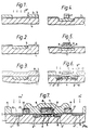
- a substrate 1 of n-type single crystal silicon is oxidised to provide a surface layer of silicon dioxide 2.
- a layer of photoresist 3 is applied and using a suitable mask (not shown) a window 4 is opened in the photoresist 3, which window 4 defines the base area (Fig. 1).
- a suitable mask not shown
- boron for example, is implanted to produce a base region 5.
- the oxide exposed through window 4 is etched using the base mask (photoresist 3) to define the area within which the emitter will be formed.
- the photoresist 3 is removed (Fig. 2).
- a layer of polysilicon 6 is then deposited (Fig. 3) and doped n+, for example with arsenic or phosphorus. Following definition of the emitter area the polysilicon 6 is dry etched to produce the structure of Fig. 4 with a substantially central n+ polysilicon mesa or emitter 7. The dry etch is controlled to give good anisotropy and high selectivity over the single crystal silicon substrate 1. We have demonstrated a selectivity of 10:1. For typical layer thickness and overetches this would lead to less than 500A (0.05 ⁇ m) of the base region being consumed during the polysilicon etch process. The structure is then provided with oxide sidewall spacers 8 (Fig. 5).
- the spacers may be produced by, for example the oxidation method described in our co-pending Application No. GB-8507600 (serial No. 2172743) or by using reactive ion etching (RIE) of a conformed deposited oxide.
- the method described in our co-pending Application involves the use of a silicon nitride capping layer on a polysilicon mesa (emitter) and oxidising the sidewalls of the mesa at a low temperature which is preferably below 900 o C in order to take full advantage of the differential oxidation ration of polysilicon and single crystal silicon.
- a photoresist layer 10 Fig.
- a collector contact region (not shown) in the substrate 1 is required together with suitable metallisation, for example, to provide external electrical contacts to the base and collector contacts regions, and to the polysilicon emitter.
- FIG. 7 A section through a complete bipolar transistor is shown in Fig. 7.
- This transistor has collector contact regions 13 in the substrate which are aligned to the emitter edges by use of polysilicon stripes (alignment mesas) 14 defined in the same masking and etching sequence as the emitter mesa 7.
- the sidewalls 17 of the stripes 14 are also oxidised as those of the emitter 7.
- a photoresist layer 15 is applied and patterned using a mask not shown to provide windows 16 for implantation of arsenic, for example, for the collector contact regions 13.
- the mask need only be a "sloppy" mask since the outermost oxidised edges of the stripes 14 define the edge of the collector contact regions and photoresist is only required to protect areas into which collector contact material is not to be implanted.
- the edge of the polysilicon stripe defines the distance between the emitter edge and the collector contact region. The device is thus fully self-aligned.
- the self-alignment of the base contact regions is thus achieved by a method which uses a single layer of polysilicon and sidewalls and is simplified in comparison with the known methods, which may use two layers of polysilicon, referred to above.
Landscapes
- Bipolar Transistors (AREA)
Claims (5)
- Procédé de fabrication d'un transistor bipolaire qui nécessite la disposition d'une seule couche de silicium polycristallin, comprenant l'exécution des étapes suivantes, dans l'ordre suivant : l'implantation d'une matière de dopage ayant un premier type de conductivité dans un substrat semi-conducteur (1) ayant l'autre type de conductivité, à travers une couche d'oxyde (2) placée sur le substrat par l'intermédiaire d'une fenêtre (4) formée dans une couche de masquage (3) afin qu'une région de base (5) soit formée dans le substrat, l'enlèvement ultérieur d'une partie au moins de la couche exposée d'oxyde (2) et l'enlèvement de la couche de masquage (3), le dépôt d'une couche (6) de silicium polycristallin comprenant une couche unique sur la région de base (5) et la couche environnante d'oxyde (2), le dopage de la couche de silicium polycristallin (6) à l'autre type de conductivité, la délimitation d'une structure mesa (7) à partir de la couche (6) de silicium polycristallin dopée, cette structure mesa (7) recouvrant une partie de la région de base et comportant un émetteur de silicium polycristallin destiné au transistor bipolaire, l'exécution d'une opération d'oxydation pendant laquelle les parois latérales au moins (8) de la structure mesa (7) sont oxydées, l'implantation d'une matière de dopage du premier type de conductivité dans le substrat (1) afin qu'une région de contacts de base (12) soit formée dans le substrat au contact de la région de base (5), l'utilisation d'au moins une paroi latérale oxydée (8) de la structure mesa comme partie du masque d'implantation si bien que la région de contacts de base (12) est automatiquement alignée sur l'émetteur (7) de silicium polycristallin, la formation d'une région (13) de contacts de collecteur de l'autre type de conductivité dans le substrat (1), et la disposition de contacts électriques externes pour la région implantée de contacts de base (12), la région de contacts de collecteur (13) et l'émetteur (7) de silicium polycristallin.
- Procédé selon la revendication 1, dans lequel la délimitation de la structure mesa comprend le masquage convenable de la couche (6) de silicium polycristallin et une attaque à sec.
- Procédé selon la revendication 1 ou 2, comprenant en outre les étapes de délimitation d'au moins une structure mesa (14) d'alignement de contacts de silicium polycristallin dans la couche (6) de silicium polycristallin, la structure mesa (14) d'alignement étant placée sur la couche d'oxyde (2) et les parois latérales (17) de cette structure mesa d'alignement (14) étant oxydées pendant l'étape d'oxydation, et d'implantation de la région de contacts de collecteur (13) dans le substrat (1) à l'aide d'au moins une paroi latérale oxydée (17) de la structure mesa d'alignement (14) constituant une partie du masque d'implantation, si bien que l'espacement de l'émetteur (7) de silicium polycristallin et de la région de contacts de collecteur (13) est déterminé par la structure mesa d'alignement (14).
- Procédé selon l'une quelconque des revendications précédentes, dans lequel la structure mesa (7) est disposée pratiquement au centre d'une surface de la région de base (5), et le procédé comprend une étape de formation de deux régions de contacts de base (12) placées de part et d'autre de la structure mesa (7) et alignées automatiquement sur celle-ci par des parois latérales oxydées respectives (8).
- Procédé selon l'une quelconque des revendications précédentes, dans lequel une autre partie du masque d'implantation des régions de contacts de base est formée par une matière de réserve photographique (10).
Applications Claiming Priority (2)
| Application Number | Priority Date | Filing Date | Title |
|---|---|---|---|
| GB8507602A GB2172744B (en) | 1985-03-23 | 1985-03-23 | Semiconductor devices |
| GB8507602 | 1985-03-23 |
Publications (3)
| Publication Number | Publication Date |
|---|---|
| EP0202727A2 EP0202727A2 (fr) | 1986-11-26 |
| EP0202727A3 EP0202727A3 (en) | 1988-03-23 |
| EP0202727B1 true EP0202727B1 (fr) | 1992-01-08 |
Family
ID=10576524
Family Applications (2)
| Application Number | Title | Priority Date | Filing Date |
|---|---|---|---|
| EP86300865A Expired - Lifetime EP0202727B1 (fr) | 1985-03-23 | 1986-02-10 | Dispositif semi-conducteur |
| EP86103384A Withdrawn EP0199061A3 (fr) | 1985-03-23 | 1986-03-13 | Dispositif semi-conducteur |
Family Applications After (1)
| Application Number | Title | Priority Date | Filing Date |
|---|---|---|---|
| EP86103384A Withdrawn EP0199061A3 (fr) | 1985-03-23 | 1986-03-13 | Dispositif semi-conducteur |
Country Status (10)
| Country | Link |
|---|---|
| US (3) | US4745080A (fr) |
| EP (2) | EP0202727B1 (fr) |
| JP (2) | JPH0812863B2 (fr) |
| KR (2) | KR940006691B1 (fr) |
| CN (2) | CN1009887B (fr) |
| DE (1) | DE3683316D1 (fr) |
| GB (1) | GB2172744B (fr) |
| IE (1) | IE57334B1 (fr) |
| IN (1) | IN166243B (fr) |
| PH (1) | PH24294A (fr) |
Families Citing this family (39)
| Publication number | Priority date | Publication date | Assignee | Title |
|---|---|---|---|---|
| GB2172744B (en) * | 1985-03-23 | 1989-07-19 | Stc Plc | Semiconductor devices |
| GB8507624D0 (en) * | 1985-03-23 | 1985-05-01 | Standard Telephones Cables Ltd | Semiconductor devices |
| US5005066A (en) * | 1987-06-02 | 1991-04-02 | Texas Instruments Incorporated | Self-aligned NPN bipolar transistor built in a double polysilicon CMOS technology |
| US4803175A (en) * | 1987-09-14 | 1989-02-07 | Motorola Inc. | Method of fabricating a bipolar semiconductor device with silicide contacts |
| US5179031A (en) * | 1988-01-19 | 1993-01-12 | National Semiconductor Corporation | Method of manufacturing a polysilicon emitter and a polysilicon gate using the same etch of polysilicon on a thin gate oxide |
| US5124817A (en) * | 1988-01-19 | 1992-06-23 | National Semiconductor Corporation | Polysilicon emitter and a polysilicon gate using the same etch of polysilicon on a thin gate oxide |
| US5001081A (en) * | 1988-01-19 | 1991-03-19 | National Semiconductor Corp. | Method of manufacturing a polysilicon emitter and a polysilicon gate using the same etch of polysilicon on a thin gate oxide |
| US4857476A (en) * | 1988-01-26 | 1989-08-15 | Hewlett-Packard Company | Bipolar transistor process using sidewall spacer for aligning base insert |
| GB8810973D0 (en) * | 1988-05-10 | 1988-06-15 | Stc Plc | Improvements in integrated circuits |
| KR910005401B1 (ko) * | 1988-09-07 | 1991-07-29 | 경상현 | 비결정 실리콘을 이용한 자기정렬 트랜지스터 제조방법 |
| JPH02170538A (ja) * | 1988-12-23 | 1990-07-02 | Toshiba Corp | 半導体装置の製造方法 |
| US4927775A (en) * | 1989-03-06 | 1990-05-22 | Motorola Inc. | Method of fabricating a high performance bipolar and MOS device |
| US4902639A (en) * | 1989-08-03 | 1990-02-20 | Motorola, Inc. | Process for making BiCMOS integrated circuit having a shallow trench bipolar transistor with vertical base contacts |
| US5008207A (en) * | 1989-09-11 | 1991-04-16 | International Business Machines Corporation | Method of fabricating a narrow base transistor |
| US5132765A (en) * | 1989-09-11 | 1992-07-21 | Blouse Jeffrey L | Narrow base transistor and method of fabricating same |
| US5268314A (en) * | 1990-01-16 | 1993-12-07 | Philips Electronics North America Corp. | Method of forming a self-aligned bipolar transistor |
| US5013671A (en) * | 1990-06-20 | 1991-05-07 | Texas Instruments Incorporated | Process for reduced emitter-base capacitance in bipolar transistor |
| US5124271A (en) * | 1990-06-20 | 1992-06-23 | Texas Instruments Incorporated | Process for fabricating a BiCMOS integrated circuit |
| US5082796A (en) * | 1990-07-24 | 1992-01-21 | National Semiconductor Corporation | Use of polysilicon layer for local interconnect in a CMOS or BiCMOS technology incorporating sidewall spacers |
| US6011283A (en) * | 1992-10-19 | 2000-01-04 | Hyundai Electronics America | Pillar emitter for BiCMOS devices |
| US5348896A (en) * | 1992-11-27 | 1994-09-20 | Winbond Electronic Corp. | Method for fabricating a BiCMOS device |
| US5320972A (en) * | 1993-01-07 | 1994-06-14 | Northern Telecom Limited | Method of forming a bipolar transistor |
| US5476800A (en) * | 1994-01-31 | 1995-12-19 | Burton; Gregory N. | Method for formation of a buried layer for a semiconductor device |
| US5476803A (en) * | 1994-10-17 | 1995-12-19 | Liu; Kwo-Jen | Method for fabricating a self-spaced contact for semiconductor devices |
| CA2166450C (fr) * | 1995-01-20 | 2008-03-25 | Ronald Salovey | Polyethylene de masse moleculaire tres elevee, reticule chimiquement, pour articulations artificielles chez l'homme |
| EP0935446B1 (fr) * | 1996-07-09 | 2007-02-07 | Orthopaedic Hospital | Reticulation du polyethylene pour limiter l'usure au moyen de traitements thermique et a rayonnement |
| SE519628C2 (sv) * | 1997-03-04 | 2003-03-18 | Ericsson Telefon Ab L M | Tillverkningsförfarande för halvledarkomponent med deponering av selektivt utformat material,vilket är ogenomträngligt för dopjoner |
| US5849613A (en) * | 1997-10-23 | 1998-12-15 | Chartered Semiconductor Manufacturing Ltd. | Method and mask structure for self-aligning ion implanting to form various device structures |
| US5904536A (en) * | 1998-05-01 | 1999-05-18 | National Semiconductor Corporation | Self aligned poly emitter bipolar technology using damascene technique |
| US6225181B1 (en) | 1999-04-19 | 2001-05-01 | National Semiconductor Corp. | Trench isolated bipolar transistor structure integrated with CMOS technology |
| US6043130A (en) * | 1999-05-17 | 2000-03-28 | National Semiconductor Corporation | Process for forming bipolar transistor compatible with CMOS utilizing tilted ion implanted base |
| US6262472B1 (en) | 1999-05-17 | 2001-07-17 | National Semiconductor Corporation | Bipolar transistor compatible with CMOS utilizing tilted ion implanted base |
| US6313000B1 (en) | 1999-11-18 | 2001-11-06 | National Semiconductor Corporation | Process for formation of vertically isolated bipolar transistor device |
| AT4149U1 (de) * | 1999-12-03 | 2001-02-26 | Austria Mikrosysteme Int | Verfahren zum herstellen von strukturen in chips |
| US6352901B1 (en) * | 2000-03-24 | 2002-03-05 | Industrial Technology Research Institute | Method of fabricating a bipolar junction transistor using multiple selectively implanted collector regions |
| DE202006017371U1 (de) * | 2006-11-13 | 2008-03-20 | Big Dutchman Pig Equipment Gmbh | Förderkette |
| JP4498407B2 (ja) | 2006-12-22 | 2010-07-07 | キヤノン株式会社 | プロセスカートリッジ、電子写真画像形成装置、及び、電子写真感光体ドラムユニット |
| WO2011018720A1 (fr) * | 2009-08-11 | 2011-02-17 | Koninklijke Philips Electronics, N.V. | Système de charge haute tension du type non magnétique destiné à être utilisé dans des dispositifs de stimulation cardiaque |
| CN109037061A (zh) * | 2018-07-26 | 2018-12-18 | 深圳市南硕明泰科技有限公司 | 一种晶体管及其制作方法 |
Family Cites Families (26)
| Publication number | Priority date | Publication date | Assignee | Title |
|---|---|---|---|---|
| NL149638B (nl) * | 1966-04-14 | 1976-05-17 | Philips Nv | Werkwijze voor het vervaardigen van een halfgeleiderinrichting bevattende ten minste een veldeffecttransistor, en halfgeleiderinrichting, vervaardigd volgens deze werkwijze. |
| JPS539469A (en) * | 1976-07-15 | 1978-01-27 | Nippon Telegr & Teleph Corp <Ntt> | Semiconductor device having electrode of stepped structure and its production |
| JPS53132275A (en) * | 1977-04-25 | 1978-11-17 | Nippon Telegr & Teleph Corp <Ntt> | Semiconductor device and its production |
| US4240195A (en) * | 1978-09-15 | 1980-12-23 | Bell Telephone Laboratories, Incorporated | Dynamic random access memory |
| JPS55123157A (en) * | 1979-03-16 | 1980-09-22 | Oki Electric Ind Co Ltd | High-stability ion-injected resistor |
| JPS5690561A (en) * | 1979-12-22 | 1981-07-22 | Fujitsu Ltd | Manufacture of semiconductor device |
| JPS56115560A (en) * | 1980-02-18 | 1981-09-10 | Toshiba Corp | Manufacture of semiconductor device |
| DE3160917D1 (en) * | 1980-03-22 | 1983-10-27 | Tokyo Shibaura Electric Co | Semiconductor device and method for fabricating the same |
| JPS56148863A (en) * | 1980-04-21 | 1981-11-18 | Nec Corp | Manufacture of semiconductor device |
| US4400865A (en) * | 1980-07-08 | 1983-08-30 | International Business Machines Corporation | Self-aligned metal process for integrated circuit metallization |
| US4691219A (en) * | 1980-07-08 | 1987-09-01 | International Business Machines Corporation | Self-aligned polysilicon base contact structure |
| JPS5936432B2 (ja) * | 1980-08-25 | 1984-09-04 | 株式会社東芝 | 半導体装置の製造方法 |
| DE3174638D1 (en) * | 1980-10-29 | 1986-06-19 | Fairchild Camera Instr Co | A method of fabricating a self-aligned integrated circuit structure using differential oxide growth |
| GB2090053B (en) * | 1980-12-19 | 1984-09-19 | Philips Electronic Associated | Mesfet |
| JPS57130461A (en) * | 1981-02-06 | 1982-08-12 | Hitachi Ltd | Semiconductor memory storage |
| JPS5852817A (ja) * | 1981-09-25 | 1983-03-29 | Hitachi Ltd | 半導体装置及びその製造方法 |
| JPS58132964A (ja) * | 1982-02-01 | 1983-08-08 | Toshiba Corp | 半導体装置の製造方法 |
| DE3272436D1 (en) * | 1982-05-06 | 1986-09-11 | Itt Ind Gmbh Deutsche | Method of making a monolithic integrated circuit with at least one isolated gate field effect transistor and one bipolar transistor |
| DE3274699D1 (en) * | 1982-09-20 | 1987-01-22 | Itt Ind Gmbh Deutsche | Method of making a monolithic integrated circuit with at least one bipolar planar transistor |
| JPS5989457A (ja) * | 1982-11-15 | 1984-05-23 | Hitachi Ltd | 半導体装置の製造方法 |
| US4521952A (en) * | 1982-12-02 | 1985-06-11 | International Business Machines Corporation | Method of making integrated circuits using metal silicide contacts |
| JPS59108361A (ja) * | 1982-12-14 | 1984-06-22 | Olympus Optical Co Ltd | 半導体装置およびその製造方法 |
| EP0122004A3 (fr) * | 1983-03-08 | 1986-12-17 | Trw Inc. | Construction d'un transistor bipolaire |
| US4529996A (en) * | 1983-04-14 | 1985-07-16 | Allied Coporation | Indium phosphide-boron phosphide heterojunction bipolar transistor |
| DE3369030D1 (en) * | 1983-04-18 | 1987-02-12 | Itt Ind Gmbh Deutsche | Method of making a monolithic integrated circuit comprising at least one insulated gate field-effect transistor |
| GB2172744B (en) * | 1985-03-23 | 1989-07-19 | Stc Plc | Semiconductor devices |
-
1985
- 1985-03-23 GB GB8507602A patent/GB2172744B/en not_active Expired
-
1986
- 1986-02-10 DE DE8686300865T patent/DE3683316D1/de not_active Expired - Fee Related
- 1986-02-10 EP EP86300865A patent/EP0202727B1/fr not_active Expired - Lifetime
- 1986-02-11 IE IE380/86A patent/IE57334B1/en not_active IP Right Cessation
- 1986-02-12 IN IN119/DEL/86A patent/IN166243B/en unknown
- 1986-02-17 KR KR1019860001082A patent/KR940006691B1/ko not_active Expired - Fee Related
- 1986-02-17 JP JP61032673A patent/JPH0812863B2/ja not_active Expired - Lifetime
- 1986-02-19 PH PH33433A patent/PH24294A/en unknown
- 1986-02-20 US US06/831,257 patent/US4745080A/en not_active Expired - Lifetime
- 1986-02-26 CN CN86101209A patent/CN1009887B/zh not_active Expired
- 1986-03-13 EP EP86103384A patent/EP0199061A3/fr not_active Withdrawn
- 1986-03-20 JP JP61061050A patent/JPS61259570A/ja active Pending
- 1986-03-22 KR KR1019860002151A patent/KR860007752A/ko not_active Withdrawn
- 1986-03-22 CN CN198686101884A patent/CN86101884A/zh active Pending
-
1988
- 1988-05-17 US US07/194,912 patent/US5055419A/en not_active Expired - Lifetime
- 1988-12-05 US US07/282,956 patent/US4916517A/en not_active Expired - Lifetime
Also Published As
| Publication number | Publication date |
|---|---|
| US4745080A (en) | 1988-05-17 |
| JPH0812863B2 (ja) | 1996-02-07 |
| JPS61229362A (ja) | 1986-10-13 |
| KR940006691B1 (ko) | 1994-07-25 |
| EP0202727A2 (fr) | 1986-11-26 |
| EP0199061A3 (fr) | 1988-03-30 |
| US4916517A (en) | 1990-04-10 |
| JPS61259570A (ja) | 1986-11-17 |
| KR860007751A (ko) | 1986-10-17 |
| CN86101884A (zh) | 1986-11-12 |
| PH24294A (en) | 1990-05-29 |
| IE860380L (en) | 1986-09-23 |
| GB2172744A (en) | 1986-09-24 |
| US5055419A (en) | 1991-10-08 |
| IE57334B1 (en) | 1992-07-29 |
| GB2172744B (en) | 1989-07-19 |
| DE3683316D1 (de) | 1992-02-20 |
| IN166243B (fr) | 1990-03-31 |
| KR860007752A (ko) | 1986-10-17 |
| EP0202727A3 (en) | 1988-03-23 |
| CN1009887B (zh) | 1990-10-03 |
| CN86101209A (zh) | 1986-09-17 |
| EP0199061A2 (fr) | 1986-10-29 |
| GB8507602D0 (en) | 1985-05-01 |
Similar Documents
| Publication | Publication Date | Title |
|---|---|---|
| EP0202727B1 (fr) | Dispositif semi-conducteur | |
| US4753898A (en) | LDD CMOS process | |
| US4784971A (en) | Process for manufacturing semiconductor BICMOS device | |
| US4503601A (en) | Oxide trench structure for polysilicon gates and interconnects | |
| US5504031A (en) | Elevated source/drain with solid phase diffused source/drain extension for deep sub-micron mosfets | |
| US4744859A (en) | Process for fabricating lightly doped drain MOS devices | |
| JPH0744272B2 (ja) | トランジスタ製造方法 | |
| JPS6226590B2 (fr) | ||
| JPH0628266B2 (ja) | 半導体装置の製造方法 | |
| JPH02125623A (ja) | 自己整合トランジスタの製造方法 | |
| US4571817A (en) | Method of making closely spaced contacts to PN-junction using stacked polysilicon layers, differential etching and ion implantations | |
| EP0409132B1 (fr) | Méthode de fabrication d'une structure comprenant des jonctions diffusées auto-alignées | |
| EP0314600B1 (fr) | Emetteur auto-aligné en polysilicium et structure de contact pour un transistor bipolaire haute performance | |
| EP0178000B1 (fr) | Procédé de formation de rainures submicroniques, par exemple dans un matériau semi-conducteur et dispositifs obtenus selon ce procédé | |
| US4619036A (en) | Self-aligned low-temperature emitter drive-in | |
| EP0421507B1 (fr) | Méthode de fabrication d'un transistor bipolaire | |
| EP0326211B1 (fr) | Dispositif semi-conducteur et procédé de fabrication de ce dispositif | |
| KR100346010B1 (ko) | 베이스 폭의 변화를 억제하기 위한 바이폴라 트랜지스터를형성하는 방법 | |
| US5747374A (en) | Methods of fabricating bipolar transistors having separately formed intrinsic base and link-up regions | |
| US6444536B2 (en) | Method for fabricating bipolar transistors | |
| JPH02295129A (ja) | 半導体装置の製造方法 | |
| JPH0640549B2 (ja) | Mos半導体装置の製造方法 | |
| JPS60216580A (ja) | 半導体装置の製造方法 | |
| JPH0630389B2 (ja) | 半導体素子 | |
| JP2546650B2 (ja) | バイポ−ラトランジスタの製造法 |
Legal Events
| Date | Code | Title | Description |
|---|---|---|---|
| PUAI | Public reference made under article 153(3) epc to a published international application that has entered the european phase |
Free format text: ORIGINAL CODE: 0009012 |
|
| AK | Designated contracting states |
Kind code of ref document: A2 Designated state(s): DE FR IT NL |
|
| RAP1 | Party data changed (applicant data changed or rights of an application transferred) |
Owner name: STC PLC |
|
| PUAL | Search report despatched |
Free format text: ORIGINAL CODE: 0009013 |
|
| RHK1 | Main classification (correction) |
Ipc: H01L 21/00 |
|
| AK | Designated contracting states |
Kind code of ref document: A3 Designated state(s): DE FR IT NL |
|
| 17P | Request for examination filed |
Effective date: 19880222 |
|
| 17Q | First examination report despatched |
Effective date: 19900712 |
|
| ITF | It: translation for a ep patent filed | ||
| RAP1 | Party data changed (applicant data changed or rights of an application transferred) |
Owner name: NORTHERN TELECOM EUROPE LIMITED |
|
| RAP1 | Party data changed (applicant data changed or rights of an application transferred) |
Owner name: NORTHERN TELECOM EUROPE LIMITED |
|
| GRAA | (expected) grant |
Free format text: ORIGINAL CODE: 0009210 |
|
| AK | Designated contracting states |
Kind code of ref document: B1 Designated state(s): DE FR IT NL |
|
| ET | Fr: translation filed | ||
| REF | Corresponds to: |
Ref document number: 3683316 Country of ref document: DE Date of ref document: 19920220 |
|
| PLBE | No opposition filed within time limit |
Free format text: ORIGINAL CODE: 0009261 |
|
| STAA | Information on the status of an ep patent application or granted ep patent |
Free format text: STATUS: NO OPPOSITION FILED WITHIN TIME LIMIT |
|
| 26N | No opposition filed | ||
| ITPR | It: changes in ownership of a european patent |
Owner name: CAMBIO RAGIONE SOCIALE;NORTHERN TELECOM EUROPE LIM |
|
| REG | Reference to a national code |
Ref country code: FR Ref legal event code: TP |
|
| NLT1 | Nl: modifications of names registered in virtue of documents presented to the patent office pursuant to art. 16 a, paragraph 1 |
Owner name: STC LIMITED TE MAIDENHEAD, GROOT-BRITTANNIE. |
|
| NLS | Nl: assignments of ep-patents |
Owner name: NORTHERN TELECOM LIMITED TE MONTREAL, CANADA. |
|
| PGFP | Annual fee paid to national office [announced via postgrant information from national office to epo] |
Ref country code: DE Payment date: 20010205 Year of fee payment: 16 |
|
| PGFP | Annual fee paid to national office [announced via postgrant information from national office to epo] |
Ref country code: FR Payment date: 20010208 Year of fee payment: 16 |
|
| PGFP | Annual fee paid to national office [announced via postgrant information from national office to epo] |
Ref country code: NL Payment date: 20010228 Year of fee payment: 16 |
|
| PG25 | Lapsed in a contracting state [announced via postgrant information from national office to epo] |
Ref country code: NL Free format text: LAPSE BECAUSE OF NON-PAYMENT OF DUE FEES Effective date: 20020901 |
|
| PG25 | Lapsed in a contracting state [announced via postgrant information from national office to epo] |
Ref country code: DE Free format text: LAPSE BECAUSE OF NON-PAYMENT OF DUE FEES Effective date: 20020903 |
|
| PG25 | Lapsed in a contracting state [announced via postgrant information from national office to epo] |
Ref country code: FR Free format text: LAPSE BECAUSE OF NON-PAYMENT OF DUE FEES Effective date: 20021031 |
|
| NLV4 | Nl: lapsed or anulled due to non-payment of the annual fee |
Effective date: 20020901 |
|
| REG | Reference to a national code |
Ref country code: FR Ref legal event code: ST |
|
| PG25 | Lapsed in a contracting state [announced via postgrant information from national office to epo] |
Ref country code: IT Free format text: LAPSE BECAUSE OF NON-PAYMENT OF DUE FEES;WARNING: LAPSES OF ITALIAN PATENTS WITH EFFECTIVE DATE BEFORE 2007 MAY HAVE OCCURRED AT ANY TIME BEFORE 2007. THE CORRECT EFFECTIVE DATE MAY BE DIFFERENT FROM THE ONE RECORDED. Effective date: 20050210 |