EP0103653B1 - Procédé de fabrication d'un circuit intégré monolithique comportant au moins un transistor bipolaire planaire - Google Patents
Procédé de fabrication d'un circuit intégré monolithique comportant au moins un transistor bipolaire planaire Download PDFInfo
- Publication number
- EP0103653B1 EP0103653B1 EP82108669A EP82108669A EP0103653B1 EP 0103653 B1 EP0103653 B1 EP 0103653B1 EP 82108669 A EP82108669 A EP 82108669A EP 82108669 A EP82108669 A EP 82108669A EP 0103653 B1 EP0103653 B1 EP 0103653B1
- Authority
- EP
- European Patent Office
- Prior art keywords
- region
- masking layer
- employing
- produced
- collector
- Prior art date
- Legal status (The legal status is an assumption and is not a legal conclusion. Google has not performed a legal analysis and makes no representation as to the accuracy of the status listed.)
- Expired
Links
- 238000004519 manufacturing process Methods 0.000 title claims description 13
- 229920002120 photoresistant polymer Polymers 0.000 claims description 39
- 230000000873 masking effect Effects 0.000 claims description 37
- 238000000034 method Methods 0.000 claims description 34
- 238000009792 diffusion process Methods 0.000 claims description 23
- 230000003647 oxidation Effects 0.000 claims description 21
- 238000007254 oxidation reaction Methods 0.000 claims description 21
- 239000004065 semiconductor Substances 0.000 claims description 15
- 230000008569 process Effects 0.000 claims description 14
- 239000000758 substrate Substances 0.000 claims description 12
- 238000002513 implantation Methods 0.000 claims description 10
- 150000002500 ions Chemical class 0.000 claims description 8
- 239000000463 material Substances 0.000 claims description 8
- 238000005468 ion implantation Methods 0.000 claims description 5
- 230000008901 benefit Effects 0.000 description 5
- 238000005530 etching Methods 0.000 description 3
- VYPSYNLAJGMNEJ-UHFFFAOYSA-N Silicium dioxide Chemical compound O=[Si]=O VYPSYNLAJGMNEJ-UHFFFAOYSA-N 0.000 description 2
- 230000007547 defect Effects 0.000 description 2
- 229910052814 silicon oxide Inorganic materials 0.000 description 2
- 230000032683 aging Effects 0.000 description 1
- 230000003321 amplification Effects 0.000 description 1
- 230000015572 biosynthetic process Effects 0.000 description 1
- 230000015556 catabolic process Effects 0.000 description 1
- 230000001427 coherent effect Effects 0.000 description 1
- 239000004020 conductor Substances 0.000 description 1
- 230000000694 effects Effects 0.000 description 1
- 238000000407 epitaxy Methods 0.000 description 1
- 230000002349 favourable effect Effects 0.000 description 1
- 239000012535 impurity Substances 0.000 description 1
- 230000010354 integration Effects 0.000 description 1
- 238000012986 modification Methods 0.000 description 1
- 230000004048 modification Effects 0.000 description 1
- 238000003199 nucleic acid amplification method Methods 0.000 description 1
- 230000009467 reduction Effects 0.000 description 1
- 238000007493 shaping process Methods 0.000 description 1
- 238000003878 thermal aging Methods 0.000 description 1
- 230000007704 transition Effects 0.000 description 1
Images

Classifications
-
- H—ELECTRICITY
- H01—ELECTRIC ELEMENTS
- H01L—SEMICONDUCTOR DEVICES NOT COVERED BY CLASS H10
- H01L21/00—Processes or apparatus adapted for the manufacture or treatment of semiconductor or solid state devices or of parts thereof
- H01L21/02—Manufacture or treatment of semiconductor devices or of parts thereof
- H01L21/027—Making masks on semiconductor bodies for further photolithographic processing not provided for in group H01L21/18 or H01L21/34
- H01L21/0271—Making masks on semiconductor bodies for further photolithographic processing not provided for in group H01L21/18 or H01L21/34 comprising organic layers
-
- H—ELECTRICITY
- H01—ELECTRIC ELEMENTS
- H01L—SEMICONDUCTOR DEVICES NOT COVERED BY CLASS H10
- H01L21/00—Processes or apparatus adapted for the manufacture or treatment of semiconductor or solid state devices or of parts thereof
- H01L21/70—Manufacture or treatment of devices consisting of a plurality of solid state components formed in or on a common substrate or of parts thereof; Manufacture of integrated circuit devices or of parts thereof
- H01L21/77—Manufacture or treatment of devices consisting of a plurality of solid state components or integrated circuits formed in, or on, a common substrate
- H01L21/78—Manufacture or treatment of devices consisting of a plurality of solid state components or integrated circuits formed in, or on, a common substrate with subsequent division of the substrate into plural individual devices
- H01L21/82—Manufacture or treatment of devices consisting of a plurality of solid state components or integrated circuits formed in, or on, a common substrate with subsequent division of the substrate into plural individual devices to produce devices, e.g. integrated circuits, each consisting of a plurality of components
- H01L21/822—Manufacture or treatment of devices consisting of a plurality of solid state components or integrated circuits formed in, or on, a common substrate with subsequent division of the substrate into plural individual devices to produce devices, e.g. integrated circuits, each consisting of a plurality of components the substrate being a semiconductor, using silicon technology
- H01L21/8222—Bipolar technology
-
- H—ELECTRICITY
- H01—ELECTRIC ELEMENTS
- H01L—SEMICONDUCTOR DEVICES NOT COVERED BY CLASS H10
- H01L27/00—Devices consisting of a plurality of semiconductor or other solid-state components formed in or on a common substrate
- H01L27/02—Devices consisting of a plurality of semiconductor or other solid-state components formed in or on a common substrate including semiconductor components specially adapted for rectifying, oscillating, amplifying or switching and having potential barriers; including integrated passive circuit elements having potential barriers
- H01L27/04—Devices consisting of a plurality of semiconductor or other solid-state components formed in or on a common substrate including semiconductor components specially adapted for rectifying, oscillating, amplifying or switching and having potential barriers; including integrated passive circuit elements having potential barriers the substrate being a semiconductor body
- H01L27/06—Devices consisting of a plurality of semiconductor or other solid-state components formed in or on a common substrate including semiconductor components specially adapted for rectifying, oscillating, amplifying or switching and having potential barriers; including integrated passive circuit elements having potential barriers the substrate being a semiconductor body including a plurality of individual components in a non-repetitive configuration
- H01L27/0611—Devices consisting of a plurality of semiconductor or other solid-state components formed in or on a common substrate including semiconductor components specially adapted for rectifying, oscillating, amplifying or switching and having potential barriers; including integrated passive circuit elements having potential barriers the substrate being a semiconductor body including a plurality of individual components in a non-repetitive configuration integrated circuits having a two-dimensional layout of components without a common active region
- H01L27/0641—Devices consisting of a plurality of semiconductor or other solid-state components formed in or on a common substrate including semiconductor components specially adapted for rectifying, oscillating, amplifying or switching and having potential barriers; including integrated passive circuit elements having potential barriers the substrate being a semiconductor body including a plurality of individual components in a non-repetitive configuration integrated circuits having a two-dimensional layout of components without a common active region without components of the field effect type
- H01L27/0647—Bipolar transistors in combination with diodes, or capacitors, or resistors, e.g. vertical bipolar transistor and bipolar lateral transistor and resistor
- H01L27/0652—Vertical bipolar transistor in combination with diodes, or capacitors, or resistors
- H01L27/0658—Vertical bipolar transistor in combination with resistors or capacitors
Definitions
- the object of the invention is therefore to provide a method according to the preamble of claim 1, which allows the production of integrated planar transistors using only four photoresist processes.
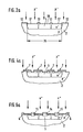
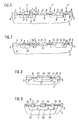
- 2a, 4a and 6a relate to production stages for the production of the lateral transistor according to FIG. 9.
- lateral transistors can also be produced without an additional photoresist process and only by modifying the four photoresist masks.
- FIG. 9 shows that the n- conductive base zone 5 consists of three overlapping sub-zones 51, 52 and 53.
- the emitter zone 14 is surrounded by the collector zone 15 and is contacted via the frame-shaped base contact zone 16 with the base contact B1, while the emitter contact E1 is attached to the emitter zone 14 and the collector contact C1 is attached to the collector zone 15.
- the integrated lateral planar transistor according to FIG. 9 is produced simultaneously with the planar transistor of part A of the monolithically integrated circuit using the same, but slightly modified, four photoresist masks at the location of the later planar transistor. These modifications result with the aid of FIGS. 2a, 4a and 6a.
- the contact holes of the lateral transistor are opened using the slightly modified third photoresist mask and the interconnect pattern required for its connection within the integrated circuit is generated using the fourth slightly modified photoresist mask.
- An arrangement according to FIG. 9 results.
- the method according to the invention has the additional advantage that integrated vertical planar transistors with “non-compensated” emitter zones can be produced.
- Such planar transistors have particularly good properties with regard to the current amplification and the transition frequency f T , as the article "Emitter Compensation Effect" in "Techn. Digest IEDM » pages 514 to 516.
Landscapes
- Engineering & Computer Science (AREA)
- Power Engineering (AREA)
- Physics & Mathematics (AREA)
- Condensed Matter Physics & Semiconductors (AREA)
- General Physics & Mathematics (AREA)
- Computer Hardware Design (AREA)
- Microelectronics & Electronic Packaging (AREA)
- Manufacturing & Machinery (AREA)
- Bipolar Transistors (AREA)
- Bipolar Integrated Circuits (AREA)
Claims (3)
Priority Applications (4)
| Application Number | Priority Date | Filing Date | Title |
|---|---|---|---|
| EP82108669A EP0103653B1 (fr) | 1982-09-20 | 1982-09-20 | Procédé de fabrication d'un circuit intégré monolithique comportant au moins un transistor bipolaire planaire |
| DE8282108669T DE3274699D1 (en) | 1982-09-20 | 1982-09-20 | Method of making a monolithic integrated circuit with at least one bipolar planar transistor |
| US06/530,526 US4509250A (en) | 1982-09-20 | 1983-09-09 | Process for manufacturing a monolithic integrated circuit comprising at least one bipolar planar transistor |
| JP58174048A JPS5976459A (ja) | 1982-09-20 | 1983-09-20 | モノリシツク集積回路の製造方法 |
Applications Claiming Priority (1)
| Application Number | Priority Date | Filing Date | Title |
|---|---|---|---|
| EP82108669A EP0103653B1 (fr) | 1982-09-20 | 1982-09-20 | Procédé de fabrication d'un circuit intégré monolithique comportant au moins un transistor bipolaire planaire |
Publications (2)
| Publication Number | Publication Date |
|---|---|
| EP0103653A1 EP0103653A1 (fr) | 1984-03-28 |
| EP0103653B1 true EP0103653B1 (fr) | 1986-12-10 |
Family
ID=8189235
Family Applications (1)
| Application Number | Title | Priority Date | Filing Date |
|---|---|---|---|
| EP82108669A Expired EP0103653B1 (fr) | 1982-09-20 | 1982-09-20 | Procédé de fabrication d'un circuit intégré monolithique comportant au moins un transistor bipolaire planaire |
Country Status (4)
| Country | Link |
|---|---|
| US (1) | US4509250A (fr) |
| EP (1) | EP0103653B1 (fr) |
| JP (1) | JPS5976459A (fr) |
| DE (1) | DE3274699D1 (fr) |
Families Citing this family (7)
| Publication number | Priority date | Publication date | Assignee | Title |
|---|---|---|---|---|
| US4586243A (en) * | 1983-01-14 | 1986-05-06 | General Motors Corporation | Method for more uniformly spacing features in a semiconductor monolithic integrated circuit |
| GB2172744B (en) * | 1985-03-23 | 1989-07-19 | Stc Plc | Semiconductor devices |
| JPS61287159A (ja) * | 1985-06-13 | 1986-12-17 | Oki Electric Ind Co Ltd | Bi−CMOS半導体IC装置の製造方法 |
| EP0430965A1 (fr) * | 1988-07-01 | 1991-06-12 | Bipolar Integrated Technology, Inc. | Procede bipolaire vlsi et transistor a trou de serrure |
| US5036016A (en) * | 1989-02-21 | 1991-07-30 | Bipolar Integrated Technology, Inc. | VLSI bipolar transistor process |
| US5061982A (en) * | 1989-02-21 | 1991-10-29 | Bipolar Integrated Technology, Inc. | VLSI triple-diffused polysilicon bipolar transistor structure |
| US8507352B2 (en) * | 2008-12-10 | 2013-08-13 | Denso Corporation | Method of manufacturing semiconductor device including insulated gate bipolar transistor and diode |
Family Cites Families (10)
| Publication number | Priority date | Publication date | Assignee | Title |
|---|---|---|---|---|
| US3891480A (en) * | 1973-10-01 | 1975-06-24 | Honeywell Inc | Bipolar semiconductor device construction |
| DE2449768A1 (de) * | 1974-10-19 | 1976-04-22 | Itt Ind Gmbh Deutsche | Verfahren zum herstellen einer monolithisch integrierten schaltung |
| JPS5946107B2 (ja) * | 1975-06-04 | 1984-11-10 | 株式会社日立製作所 | Mis型半導体装置の製造法 |
| FR2417854A1 (fr) * | 1978-02-21 | 1979-09-14 | Radiotechnique Compelec | Transistor comportant une zone resistive integree dans sa region d'emetteur |
| US4269636A (en) * | 1978-12-29 | 1981-05-26 | Harris Corporation | Method of fabricating self-aligned bipolar transistor process and device utilizing etching and self-aligned masking |
| JPS55138267A (en) * | 1979-04-12 | 1980-10-28 | Matsushita Electric Ind Co Ltd | Manufacture of semiconductor integrated circuit containing resistance element |
| US4311532A (en) * | 1979-07-27 | 1982-01-19 | Harris Corporation | Method of making junction isolated bipolar device in unisolated IGFET IC |
| JPS5656663A (en) * | 1979-10-16 | 1981-05-18 | Nec Corp | Semiconductor device |
| US4317690A (en) * | 1980-06-18 | 1982-03-02 | Signetics Corporation | Self-aligned double polysilicon MOS fabrication |
| DE3115029A1 (de) * | 1981-04-14 | 1982-11-04 | Deutsche Itt Industries Gmbh, 7800 Freiburg | "verfahren zur herstellung eines integrierten bipolaren planartransistors" |
-
1982
- 1982-09-20 DE DE8282108669T patent/DE3274699D1/de not_active Expired
- 1982-09-20 EP EP82108669A patent/EP0103653B1/fr not_active Expired
-
1983
- 1983-09-09 US US06/530,526 patent/US4509250A/en not_active Expired - Fee Related
- 1983-09-20 JP JP58174048A patent/JPS5976459A/ja active Pending
Also Published As
| Publication number | Publication date |
|---|---|
| JPS5976459A (ja) | 1984-05-01 |
| DE3274699D1 (en) | 1987-01-22 |
| EP0103653A1 (fr) | 1984-03-28 |
| US4509250A (en) | 1985-04-09 |
Similar Documents
| Publication | Publication Date | Title |
|---|---|---|
| EP0239652B1 (fr) | Procédé pour fabriquer un circuit intégré monolithique comportant au moins un transistor planaire bipolaire | |
| EP0036634B1 (fr) | Procédé de fabrication d'une structure de transistor bipolaire | |
| DE69328758T2 (de) | Verfahren zur Herstellung von SOI-Bipolar- und MOS-Transistoren | |
| DE2212049C2 (de) | Verfahren zur Herstellung einer Halbleiteranordnung und Verfahren zur Herstellung eines Transistors | |
| DE69025805T2 (de) | Herstellen von Halbleitervorrichtungen | |
| DE3205022A1 (de) | Verfahren zum herstellen einer integrierten halbleiterschaltung | |
| EP0007923B1 (fr) | Procédé pour la fabrication d'un transistor latéral à double diffusion et d'un transistor complémentaire vertical, intégré avec le premier | |
| DE4445345C2 (de) | Verfahren zur Herstellung eines Bipolartransistors | |
| EP0093786B1 (fr) | Procédé de fabrication d'un circuit intégré monolithique comportant au moins un transistor à effet de champ à porte isolée et un transistor bipolair | |
| DE2732184A1 (de) | Halbleitervorrichtung und verfahren zu ihrer herstellung | |
| DE69505348T2 (de) | Hochspannungs-MOSFET mit Feldplatten-Elektrode und Verfahren zur Herstellung | |
| DE3823270A1 (de) | Halbleiteranordnung und verfahren zu ihrer herstellung | |
| DE69122598T2 (de) | Integrierte Struktur eines bipolaren Leistungstransistors und eines Wiederspannungsbipolartransistors in Emittorschaltungs- oder Halbbrückenanordnung und dies bezügliche Herstellungsverfahren | |
| DE1564218A1 (de) | Verfahren zur Herstellung von Transistoren | |
| EP0129045A1 (fr) | Procédé de fabrication d'un transistor à effet de champ intégré ayant une couche isolante avec des contacts auto-alignés par rapport à l'électrode de grille | |
| DE1614383A1 (de) | Halbleiterbauelement und Verfahren zu seiner Herstellung | |
| DE1810322A1 (de) | Halbleiterbauelement mit einer Vielzahl von streifenfoermigen zueinander parallelen Emitterbereichen und mit mehreren Kontaktierungsebenen und Verfahren zu seiner Herstellung | |
| EP0103653B1 (fr) | Procédé de fabrication d'un circuit intégré monolithique comportant au moins un transistor bipolaire planaire | |
| DE69022710T2 (de) | Verfahren zum Herstellen einer Halbleitervorrichtung. | |
| EP0122313A1 (fr) | Procédé de fabrication d'un circuit intégré monolitique comportant au moins un transistor à effet de champ à grille isolée | |
| DE2157633A1 (de) | Verfahren zur planaren diffusion von zonen einer monolithisch integrierten festkoerperschaltung | |
| DE2752335B2 (de) | Verfahren zur Herstellung eines Sperrschicht-Feldeffekttransistors mit einem vertikalen Kanal | |
| DE68925150T2 (de) | Bipolartransistor und Verfahren zu dessen Herstellung | |
| EP0028786A1 (fr) | Procédé d'implantation d'ions | |
| EP0270703B1 (fr) | Procédé de fabrication d'un circuit intégré monolithique comprenant au moins un transistor bipolaire plan |
Legal Events
| Date | Code | Title | Description |
|---|---|---|---|
| PUAI | Public reference made under article 153(3) epc to a published international application that has entered the european phase |
Free format text: ORIGINAL CODE: 0009012 |
|
| AK | Designated contracting states |
Designated state(s): DE FR GB IT NL |
|
| 17P | Request for examination filed |
Effective date: 19840504 |
|
| GRAA | (expected) grant |
Free format text: ORIGINAL CODE: 0009210 |
|
| AK | Designated contracting states |
Kind code of ref document: B1 Designated state(s): DE FR GB IT NL |
|
| ITF | It: translation for a ep patent filed | ||
| REF | Corresponds to: |
Ref document number: 3274699 Country of ref document: DE Date of ref document: 19870122 |
|
| ET | Fr: translation filed | ||
| PLBE | No opposition filed within time limit |
Free format text: ORIGINAL CODE: 0009261 |
|
| STAA | Information on the status of an ep patent application or granted ep patent |
Free format text: STATUS: NO OPPOSITION FILED WITHIN TIME LIMIT |
|
| 26N | No opposition filed | ||
| ITTA | It: last paid annual fee | ||
| REG | Reference to a national code |
Ref country code: FR Ref legal event code: DL |
|
| PGFP | Annual fee paid to national office [announced via postgrant information from national office to epo] |
Ref country code: GB Payment date: 19931027 Year of fee payment: 12 |
|
| PG25 | Lapsed in a contracting state [announced via postgrant information from national office to epo] |
Ref country code: GB Effective date: 19940920 |
|
| GBPC | Gb: european patent ceased through non-payment of renewal fee |
Effective date: 19940920 |
|
| PGFP | Annual fee paid to national office [announced via postgrant information from national office to epo] |
Ref country code: FR Payment date: 19970820 Year of fee payment: 16 |
|
| PGFP | Annual fee paid to national office [announced via postgrant information from national office to epo] |
Ref country code: NL Payment date: 19970821 Year of fee payment: 16 |
|
| PGFP | Annual fee paid to national office [announced via postgrant information from national office to epo] |
Ref country code: DE Payment date: 19970912 Year of fee payment: 16 |
|
| REG | Reference to a national code |
Ref country code: FR Ref legal event code: TP Ref country code: FR Ref legal event code: CD Ref country code: FR Ref legal event code: CA |
|
| NLS | Nl: assignments of ep-patents |
Owner name: MICRONAS SEMICONDUCTOR HOLDING AG |
|
| NLT1 | Nl: modifications of names registered in virtue of documents presented to the patent office pursuant to art. 16 a, paragraph 1 |
Owner name: ITT MANUFACTURING ENTERPRISES, INC. |
|
| PG25 | Lapsed in a contracting state [announced via postgrant information from national office to epo] |
Ref country code: NL Free format text: LAPSE BECAUSE OF NON-PAYMENT OF DUE FEES Effective date: 19990401 |
|
| PG25 | Lapsed in a contracting state [announced via postgrant information from national office to epo] |
Ref country code: FR Free format text: LAPSE BECAUSE OF NON-PAYMENT OF DUE FEES Effective date: 19990531 |
|
| NLV4 | Nl: lapsed or anulled due to non-payment of the annual fee |
Effective date: 19990401 |
|
| PG25 | Lapsed in a contracting state [announced via postgrant information from national office to epo] |
Ref country code: DE Free format text: LAPSE BECAUSE OF NON-PAYMENT OF DUE FEES Effective date: 19990701 |
|
| REG | Reference to a national code |
Ref country code: FR Ref legal event code: ST |