EP0157202A1 - Pulsgenerator mit digitaler Pulsweitenmodulation - Google Patents
Pulsgenerator mit digitaler Pulsweitenmodulation Download PDFInfo
- Publication number
- EP0157202A1 EP0157202A1 EP85102483A EP85102483A EP0157202A1 EP 0157202 A1 EP0157202 A1 EP 0157202A1 EP 85102483 A EP85102483 A EP 85102483A EP 85102483 A EP85102483 A EP 85102483A EP 0157202 A1 EP0157202 A1 EP 0157202A1
- Authority
- EP
- European Patent Office
- Prior art keywords
- pulse
- signal
- pattern data
- sine wave
- triangle
- Prior art date
- Legal status (The legal status is an assumption and is not a legal conclusion. Google has not performed a legal analysis and makes no representation as to the accuracy of the status listed.)
- Granted
Links
Images


Classifications
-
- H—ELECTRICITY
- H02—GENERATION; CONVERSION OR DISTRIBUTION OF ELECTRIC POWER
- H02P—CONTROL OR REGULATION OF ELECTRIC MOTORS, ELECTRIC GENERATORS OR DYNAMO-ELECTRIC CONVERTERS; CONTROLLING TRANSFORMERS, REACTORS OR CHOKE COILS
- H02P27/00—Arrangements or methods for the control of AC motors characterised by the kind of supply voltage
- H02P27/04—Arrangements or methods for the control of AC motors characterised by the kind of supply voltage using variable-frequency supply voltage, e.g. inverter or converter supply voltage
-
- H—ELECTRICITY
- H02—GENERATION; CONVERSION OR DISTRIBUTION OF ELECTRIC POWER
- H02M—APPARATUS FOR CONVERSION BETWEEN AC AND AC, BETWEEN AC AND DC, OR BETWEEN DC AND DC, AND FOR USE WITH MAINS OR SIMILAR POWER SUPPLY SYSTEMS; CONVERSION OF DC OR AC INPUT POWER INTO SURGE OUTPUT POWER; CONTROL OR REGULATION THEREOF
- H02M7/00—Conversion of ac power input into dc power output; Conversion of dc power input into ac power output
- H02M7/42—Conversion of dc power input into ac power output without possibility of reversal
- H02M7/44—Conversion of dc power input into ac power output without possibility of reversal by static converters
- H02M7/48—Conversion of dc power input into ac power output without possibility of reversal by static converters using discharge tubes with control electrode or semiconductor devices with control electrode
- H02M7/53—Conversion of dc power input into ac power output without possibility of reversal by static converters using discharge tubes with control electrode or semiconductor devices with control electrode using devices of a triode or transistor type requiring continuous application of a control signal
- H02M7/537—Conversion of dc power input into ac power output without possibility of reversal by static converters using discharge tubes with control electrode or semiconductor devices with control electrode using devices of a triode or transistor type requiring continuous application of a control signal using semiconductor devices only, e.g. single switched pulse inverters
- H02M7/5387—Conversion of dc power input into ac power output without possibility of reversal by static converters using discharge tubes with control electrode or semiconductor devices with control electrode using devices of a triode or transistor type requiring continuous application of a control signal using semiconductor devices only, e.g. single switched pulse inverters in a bridge configuration
- H02M7/53871—Conversion of dc power input into ac power output without possibility of reversal by static converters using discharge tubes with control electrode or semiconductor devices with control electrode using devices of a triode or transistor type requiring continuous application of a control signal using semiconductor devices only, e.g. single switched pulse inverters in a bridge configuration with automatic control of output voltage or current
- H02M7/53873—Conversion of dc power input into ac power output without possibility of reversal by static converters using discharge tubes with control electrode or semiconductor devices with control electrode using devices of a triode or transistor type requiring continuous application of a control signal using semiconductor devices only, e.g. single switched pulse inverters in a bridge configuration with automatic control of output voltage or current with digital control
-
- H—ELECTRICITY
- H02—GENERATION; CONVERSION OR DISTRIBUTION OF ELECTRIC POWER
- H02M—APPARATUS FOR CONVERSION BETWEEN AC AND AC, BETWEEN AC AND DC, OR BETWEEN DC AND DC, AND FOR USE WITH MAINS OR SIMILAR POWER SUPPLY SYSTEMS; CONVERSION OF DC OR AC INPUT POWER INTO SURGE OUTPUT POWER; CONTROL OR REGULATION THEREOF
- H02M7/00—Conversion of ac power input into dc power output; Conversion of dc power input into ac power output
- H02M7/42—Conversion of dc power input into ac power output without possibility of reversal
- H02M7/44—Conversion of dc power input into ac power output without possibility of reversal by static converters
- H02M7/48—Conversion of dc power input into ac power output without possibility of reversal by static converters using discharge tubes with control electrode or semiconductor devices with control electrode
- H02M7/53—Conversion of dc power input into ac power output without possibility of reversal by static converters using discharge tubes with control electrode or semiconductor devices with control electrode using devices of a triode or transistor type requiring continuous application of a control signal
- H02M7/537—Conversion of dc power input into ac power output without possibility of reversal by static converters using discharge tubes with control electrode or semiconductor devices with control electrode using devices of a triode or transistor type requiring continuous application of a control signal using semiconductor devices only, e.g. single switched pulse inverters
- H02M7/5387—Conversion of dc power input into ac power output without possibility of reversal by static converters using discharge tubes with control electrode or semiconductor devices with control electrode using devices of a triode or transistor type requiring continuous application of a control signal using semiconductor devices only, e.g. single switched pulse inverters in a bridge configuration
- H02M7/53871—Conversion of dc power input into ac power output without possibility of reversal by static converters using discharge tubes with control electrode or semiconductor devices with control electrode using devices of a triode or transistor type requiring continuous application of a control signal using semiconductor devices only, e.g. single switched pulse inverters in a bridge configuration with automatic control of output voltage or current
- H02M7/53875—Conversion of dc power input into ac power output without possibility of reversal by static converters using discharge tubes with control electrode or semiconductor devices with control electrode using devices of a triode or transistor type requiring continuous application of a control signal using semiconductor devices only, e.g. single switched pulse inverters in a bridge configuration with automatic control of output voltage or current with analogue control of three-phase output
- H02M7/53876—Conversion of dc power input into ac power output without possibility of reversal by static converters using discharge tubes with control electrode or semiconductor devices with control electrode using devices of a triode or transistor type requiring continuous application of a control signal using semiconductor devices only, e.g. single switched pulse inverters in a bridge configuration with automatic control of output voltage or current with analogue control of three-phase output based on synthesising a desired voltage vector via the selection of appropriate fundamental voltage vectors, and corresponding dwelling times
-
- Y—GENERAL TAGGING OF NEW TECHNOLOGICAL DEVELOPMENTS; GENERAL TAGGING OF CROSS-SECTIONAL TECHNOLOGIES SPANNING OVER SEVERAL SECTIONS OF THE IPC; TECHNICAL SUBJECTS COVERED BY FORMER USPC CROSS-REFERENCE ART COLLECTIONS [XRACs] AND DIGESTS
- Y10—TECHNICAL SUBJECTS COVERED BY FORMER USPC
- Y10S—TECHNICAL SUBJECTS COVERED BY FORMER USPC CROSS-REFERENCE ART COLLECTIONS [XRACs] AND DIGESTS
- Y10S388/00—Electricity: motor control systems
- Y10S388/907—Specific control circuit element or device
- Y10S388/912—Pulse or frequency counter
-
- Y—GENERAL TAGGING OF NEW TECHNOLOGICAL DEVELOPMENTS; GENERAL TAGGING OF CROSS-SECTIONAL TECHNOLOGIES SPANNING OVER SEVERAL SECTIONS OF THE IPC; TECHNICAL SUBJECTS COVERED BY FORMER USPC CROSS-REFERENCE ART COLLECTIONS [XRACs] AND DIGESTS
- Y10—TECHNICAL SUBJECTS COVERED BY FORMER USPC
- Y10S—TECHNICAL SUBJECTS COVERED BY FORMER USPC CROSS-REFERENCE ART COLLECTIONS [XRACs] AND DIGESTS
- Y10S388/00—Electricity: motor control systems
- Y10S388/907—Specific control circuit element or device
- Y10S388/915—Sawtooth or ramp waveform generator
Definitions
- the present invention relates generally to a digital pulse-width-modulated pulse generator and more specifically to the pulse generator for generating a PWMed pulse signal synchronizing with a sine wave by PWMin g a sine wave signal in dependence upon a triangular wave signal in digital fashion.
- the digital PWMed pulse generator according to the present invention is advantaneously incorporated with a decoupled-vector control induction motor driving system by way of typical example.
- an analog PWMed pulse generator has generally been used for generating a PWMed pulse synchronizing with a sine wave.
- the prior-art pulse generator since the amplitude of a sine wave signal is compared with that of a triangular wave signal in analog fashion by a comparator, whenever ambient temperature varies, the amplitudes of both the signals change and further an offset voltage of the comparator inevitably fluctuates. Therefore, it is impossible to generate an accurate PWMed signal.
- the voltage and the frequency of the PWMed pulse is small, it is very difficult to generate a PWMed signal accurately.
- the generator may be increased in size, cost, the number of elements, etc.
- the method of driving an induction motor has been highly developed owing to a remarkable progress in power electronic device technology.
- the vector control method has been proposed for driving an induction motor at variable speeds under quick response characteristics equivalent to a DC machine.
- the primary current of an induction motor is divided into a primary exciting current to generate the secondary magnetic flux and a primary driving current to generate the secondary driving current, and further the vectors of the secondary magnetic flux and the secondary driving current are so controlled independently as to meet at right angles to each other.
- the magnitude of the secondary magnetic flux is controlled at a constant level and the secondary driving current is increased or decreased independently as in a DC motor.
- the induction motor is driven by an inverter activated by a PWMed pulse (for each phase).
- a PWMed pulse for each phase.
- the PWMed pulse is generated in analog fashion by comparing a sine wave signal generated by an analog sine wave generator with a triangular wave signal generated by an analog triangular wave generator, it is difficult to generate an accurate PWMed pulse.
- a phase difference command signal is applied to the control system, it is impossible to control the phase difference at high response speed on the basis of relatively simple calculations.
- the digital PWMed pulse generator with a decoupled-vector control induction motor driving system in order to control an induction motor at high response speed throughout a wide speed range and a wide torque range.
- the digital PWMed pulse generator for generating a PWMed pulse synchronizing with a sine wave signal comprises: (a) means for generating plural series of digital pattern data determined by pulse-width-modulating a sine wave having a basic frequency and a basic amplitude in dependence upon a triangular carrier wave having a frequency integer times higher than that of the sine wave and an amplitude equal to that of the sine wave, the pattern data being classified into each series by the number of triangles included within a half cycle of the sine wave, (b) means for selecting an appropriate series of digital pattern data classified by the number of triangles in response to an angular frequency command, (c) means for calculating other pattern data corresponding to another sine wave signal having an amplitude smaller than that of the selected pattern data in response to a voltage control ratio command, and (d) means for generating a pulse-width-modulated pulse on the basis of the calculated pattern data.
- PWMed pulse width modulated
- Fig. 1 shows an example of the prior-art PWMed pulse generator, which generates a PWMed pulse in analog fashion on the basis of a sine wave signal and a triangular wave signal having a frequency several times higher than that of the sine wave signal.
- the generator includes a sine wave generator 1, a triangular wave generator 2, a multiplier 3, and a comparator 4.
- the sine wave generator 1 generates a first sine wave signal having a constant amplitude and a frequency equal to an angular frequency command signal w 0 .
- the triangular wave generator 2 generates a triangular wave (carrier) signal having the same constant amplitude as that of the sine wave signal and a frequency n times higher than the angular frequency command signal w 0 .
- the comparator 4 compares the second sine wave signal with the triangular wave signal and outputs a logically high level signal when the second sine wave signal exceeds the triangular wave signal in voltage level and a logically low level signal when the triangular wave signal exceeds the second sine wave signal in voltage level. Therefore, the lower the amplitude of the second sine wave signal, the narrower the pulse width (high-level) of the PWMed signal.
- the generator comprises a pulse pattern generator 5, a pattern selector 6, a PWM calculator 7, and a logic gate circuit 8 in order to generate three-phase PWMed pulses.
- the generated PWMed pulses trigger each switching element in an inverter 9 to drive an induction motor 10.
- the pulse pattern generator 5 generates plural series of basic digital pattern data 6 determined by pulse-width-modulating a sine wave having a basic frequency w B and a basic amplitude in dependence upon a triangular carrier wave having a frequency integer times higher than that of the sine wave and an amplitude equal to that of the sine wave. Further, the plural series of the pattern data ⁇ n are classified by the number P of trianles included within a half cycle of the sine wave. In general, the number P is increased with decreasing sine wave frequency.
- the data selector 6 selects a series of pattern data ⁇ n determined by PWMing the basic sine wave on the basis of triangles of an appropriate number P in response to an angular frequency command w 0 .
- the PWM calculator 7 calculates another series of pattern data ⁇ x corresponding to an amplitude smaller than the basic amplitude in response a voltage control ratio command ( ⁇ 1), additionally and time pattern data t n corresponding to time intervals between each triangle-apex to each nearest intersection point between sine wave and triangular wave.
- the calculator 7 further generates triangle slop data D s (positive slope and negative slope) and a half period T/2 of the triangular wave.
- the logic gate circuit 8 generates each phase PWMed signal e a , e b , e c on the basis of the calculated time pattern data t n , the generated triangle slope data D s and the half period T/2. Further, in Fig. 2, symbol WR designates a write command; symbol INT designates an interruption command.
- the pulse pattern generator 5 generates plural series of basic digital pattern data ⁇ n being classified by the number P of triangular (carrier) wave included within a half period of a sine wave.
- the above basic means that the amplitude of the sine wave is equal to that of the triangular wave.
- the above pulse pattern generator 5 is made up of read-only-memory units, for instance.
- the voltage control ratio ⁇ is expressed as follows:
- the number P of carrier signals included within a half period of a sine wave SIN w B t is determined to be multiples of three as follows: This is because it is possible to perfectly synchronize the triangular wave with the sine wave while eliminating the harmful influence due to higher harmonics.
- the PWMed pulse between the two are also shown in Fig. 4(B).
- the logically high voltage levels of the PWMed pulse correspond to ranges within which the amplitude of the sine wave exceeds that of the triangular wave.
- P 1 to P 9 denotes a series of sampling.points of pattern data ⁇ n .
- the high level of the PWMed pulse can be obtained, when each point of intersection between the two waves is determined.
- a series of the basic pattern data ⁇ n ( ⁇ 1 , ⁇ 2 , ...) are angular intervals from each sampling point P n (P 1 , P 2 , ...) (intersections between the triangular wave and the abscissa) to each point of intersection between the two waves.
- the above pattern data ⁇ n are listed in tables being classified according to the number P of triangles included within a half cycle of the sine wave.
- ⁇ n can simply be calculated as follows: where e x denotes pattern data determined when ⁇ is not 1.
- the above expression (3) indicates ⁇ x is proportional to e n . This is because it is possible to consider that each part of the sine wave corresponding to ⁇ n (from P n to an intersection between the two waves) is approximately linear within a relatively short angular intervals Further, in the case ⁇ >1, e x is partially further corrected in the expression (3).
- the above pattern data e x is further calculated in order to transform the data ⁇ x into data ey representative of each angular interval between each triangle apex to each point of intersection between the two waves.
- Fig. 4(A) indicates that when the triangular wave slope is positive, the PWMed pulse is at high level within the angular ranges ⁇ yn ; however, when the triangular wave slope is negative, the PWMed pulse is at low level within the angular range ⁇ yn .
- the logical gate section 8 On the basis of pattern data t n which have been calculated in response to an angular frequency command w 0 and a voltage control ratio ⁇ , the logical gate section 8 generates a PWMed pulse as explained below: With reference to Fig. 3, the logical gate section 8 comprises a first programmable timer circuit 21 including a counter T 11 and a monostable multivibrator T12, a triangle slope latch circuit 22 including two flip-flops, a second programmable timer circuit 23 including three-phase counters T 13 , T 14 and T 15 , and a logic circuit 24 including inverters, AND gates and OR gates.
- the first programmable timer circuit 21 serves to generate a triangle apex timing signal S ta as shown in Fig. 5, being connected to the PWM calculator 7A (shown as a CPU in Fig. 3) through a bus 7B.
- the first programmable timer circuit 21 includes the counter T 11 and the monostable multivibrator T 12 .
- a time value T/2 (corresponding to a half period of the triangular wave signal) is set to the first counter T 11 from the CPU 7A periodically. This time value T/2 is counted down by a series of clock pulses. Therefore, the counter T 11 generates a pulse timing signal for each half cycle of the triangular wave signal.
- the monostable multivibrator T 12 is triggered by this pulse timing signal and generates a series of triangle apex timing pulse S ta .
- the short pulse width of the timing pulse S ta is determined by the monostable multivibrator T 12 on the basis of the number of clock signals CLK.
- the triangle slope latch circuit 22 includes a first flip-flop FF 1 and a second flip-flop FF 2 .
- a triangle slope data D ("1" in positive slope, "0" in negative slope) outputted from the CPU 7A is latched by the first FF 1 in response to a command signal WRITE outputted from the CPU 7A.
- the latched triangle slope data signal D S is further latched by the second FF 2 in response to the triangle apex signal S ta outputted from the monostable multivibrator T 12 . Therefore, the second FF 2 outputs a triangle slope signal S ts , as shown in Fig. 5, from the Q terminal thereof. That is, the signal S ts is at a logically high level at positive triangle slope but at a logically low level at negative triangle slope. Further, an inverted triangle slope signal S ts is outputted simultaneously from the Q terminal of the FF 2 .
- the second programmable timer circuit 23 serves to generate three-phase triangle apex-to-intersection signals T na , T nb , T nc (only T na is shown in Fig. 5).
- the second programmable timer circuit 23 includes a second counter T 13 , a third counter T 14 and a fourth counter T 15 , each being allocated to each phase.
- Each-phase pattern data t (corresponding to time intervals from triangle apexes to intersection points between triangular wave and sine wave) are sequentially set to each counter in response to the triangle apex timing signal S ta outputted from the monostable multivibrator T 12 .
- the set time interval t n is counted down by a series of clock pulses. Therefore, each counter T 13 , T 14 or T 15 generates each apex-to-intersection signal T n , which rises at triangular apexes and falls at points of intersection between the two waves.
- Data transfer between the CPU 7A and the triangle slope latch circuit 22, the first and second programmable timer circuits 21, 23 is implemented by applying the triangle apex timing signal S ta to the CPU 7A as an interruption signal INTR.
- the logic circuit 24 On the basis of the triangle slope signals Sts, S ts and the apex-to-intersection signals T na , T nb , T nc , the logic circuit 24 generates each-phase PWMed pulse signal e a , e b , or e c respectively. The operation of the logic circuit 24 will be described with respect to only a-phase hereinbelow.
- a first AND gate G 1 generates a signal E a + by AND ing the positive triangle slope signal S ts and the apex-to-intersection signal T na . Therefore, E a + is at high level in positive triangle slopes within the ranges between triangle apexes and intersections between two waves.
- a second AND gate G 2 generates a signal E a - by AND ing the negative triangle slope signal S ts and the apex-to-intersection signal T na inversed by a first inverter INV 1. Therefore, E a - is at high level in negative triangle slopes within the ranges between triangle apexes to intersections between two waves.
- each-phase PWMed voltage pulse e a , e b , or e c by determining each real time apex-to-intersection data T n for each half period T/2 of the triangle wave signal.
- the envelope frequency f o (motor-driving inverter frequency) of the PWMed pulse can be expressed as where T denotes a period of the triangular wave; P denotes the number of triangles included within a half cycle of the sine wave.
- the inverter 9 In response to the PWMed pulse signals e a , e b , e c , the inverter 9 is activated to drive the induction motor 10 in accordance with a voltage control ratio command ⁇ and an angular frequency command w 0 .
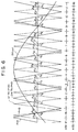
- the motor 10 is driven clockwise, for instance: in the case where the pattern data ⁇ n are read in the order of ⁇ 18 , ⁇ 17 , ... ⁇ 3 , ⁇ 2 , ⁇ 1 , ⁇ 18 , the motor 10 is driven counterclockwise. That is to say, the rotational direction of the induction motor 10 can be driven in either direction by switching the sampling order of the pattern data ⁇ n . For instance, if the motor 10 is required to switch the motor rotational direction at sampling point 3 in Fig. 6, for instance, the data are read or sampled as follows: ⁇ 1 , ⁇ 2 , ⁇ 3 , ⁇ 2 , ⁇ 1 , ⁇ 18 ...
- n denotes the sampling points of pattern data
- phase difference command signal 0 is inputted to the CPU 7A.
- Fig. 7 shows an example of the case where a 45-degree phase difference occurs in the pattern data having nine triangles within a half cycle of the sine wave.
- the second sine wave leads the first sine wave by a phase angle of 45 degrees.
- the above phase difference is detected and calculated by another element and applied to the PWM calculator 7 as a phase difference command signal 0.
- the CPU 7A (calculating section 7) reads angular pattern data ⁇ n in sequence and outputs the calculated time pattern data t in response to the triangle apex timing signal S ta . Therefore, it is possible to reduce the phase difference by selecting an appropriate sampling position at which pattern data are read.
- Fig. 7 shows an example of the case where a 45-degree phase difference occurs in the pattern data having nine triangles within a half cycle of the sine wave.
- the second sine wave leads the first sine wave by a phase angle of 45 degrees.
- the above phase difference is detected and calculated by another element and applied to the PWM calculator 7 as a phase difference command signal 0.
- the CPU 7A
- ⁇ T /2 denotes a half angular period of the triangular wave
- AN denotes an increment or decrement from the sampling position n at which the present data is read
- ⁇ denotes a remainder.
- the new sampling position n new can be expressed under consideration of the motor rotational direction and the phase difference as follows:
- phase difference ⁇ can be corrected as follows:
- T/2 corresponds to ⁇ T /2
- the half period T/2 corresponds to ⁇ T /2
- ⁇ denotes a time corresponding to angular phase remainder.
- phase difference command signal is inputted, it is possible to provide a phase difference to the PWMed signal at high response speed by skipping or returning the sampling position (AN) and further adjusting the triangle half period (T/2) and the pattern data (t n ) both first set in the counters T 11 , T 13 , T 14 , and T 15 .
- the operation of the PWMed pulse generator according to the present invention will be described hereinbelow.
- the CPU 7A shown in Fig. 3 includes the pulse pattern generator 5, the data selector 6 and the PWM calculator 7.
- a basic sine wave SIN w B t and the number P of triangles included within a half cycle of the sine wave are both determined.
- step S 3 if there exists ⁇ , this value is temporarily stored for adjusting the time pattern data t n and the half period of trianglar wave T/2 later.
- Control reads a-phase angular pattern data ⁇ na determined on the basis of the angular frequency command w 0 and the corresponding number P from the ROM arranged in the CPU 7A (in step S 4 ).
- Fig. 9 is a block diagram showing an example of application of the digital PWMed pulse generator according to the present invention to a decoupled-vector control induction motor driving system.
- this driving system the primary current corresponding to the secondary magnetic flux and the primary current corresponding to the secondary driving current are controlled independently in such a way that these two vectors meet at right angles to each other.
- the above-mentioned decoupled-vector implies that the mutual interference produced between the secondary magnetic flux and secondary driving current is cancelled out.
- an induction motor can be treated mathematically as a simplified model in dependence upon two-axis theory.
- all three-phase electrical values including those on the secondary side are transformed into two-phase electrical values on the primary side, on the assumption that higher harmonics, iron loss, magnetic saturation and so on are all ignored and signals are trigonometric function.
- the above expression (I) indicates the relationship between the primary voltage and the primary current and the relationship between the secondary voltage and the secondary magnetic flux, while including phase relationship.
- the above expression indicates that the secondary magnetic flux ⁇ 2 ⁇ is controlled at a contract value only on the a-axis and the secondary driving current i 2 ⁇ is variably controlled only on the ⁇ -axis, as in a DC motor.
- the primary current a-axis component i 1 ⁇ corresponds to the secondary magnetic flux ⁇ 2 ⁇ and the primary current ⁇ -axis component i 1 ⁇ corresponds to the secondary driving current i 2 p.
- the value L w o 0 I* 1 ⁇ obtained by multiplying the reference primary current i * la by supply voltage angular frequency w o and coefficient L 1 is added to the value r 1 i 1 ⁇ obtained by multiplying the primary current i 1 ⁇ by the primary resistance r l .
- slip frequency w s is proportional to the primary current i 1 ⁇ .
- the values of the primary current i 1 ⁇ corresponding to the secondary flux ⁇ 2 ⁇ and the primary current i 1 ⁇ corresponding to the secondary current i 2 ⁇ are necessary for controlling information in addition to rotor angular frequency w n . It is more practical to use reference or command values in the actual control.
- the reference primary current i* 1 ⁇ can be obtained on the basis of the reference secondary flux ⁇ * 2 ⁇ as follows:
- the primary current i 1 ⁇ can be obtained on the basis of both the reference torque T * and the reference secondary flux ⁇ * 2 ⁇ as follows:
- the secondary reference flux ⁇ * 2 ⁇ is constant and therefore the reference torque T * can be determined by the primary current i 1 ⁇ obtained through the PI speed control amplifier (proportional integrator) by which the difference between the reference rotor angular velocity w * n and the actual rotor angular velocity w are integrated.
- PI speed control amplifier proportional integrator
- the decoupled-vector control motor driving system includes the digital PWMed pulse generator according to the present invention, which is made up of the pulse pattern generator 5, the data selector 6, the PWM calculator 7, and the logic gate circuit 8, as already described in detail.
- the system further includes a motor speed sensor 30, a frequency-voltage converter 31, a subtractor 32, a speed control amplifier (proportional integrator) 33, a slip frequency calculator 34, an adder 35, a decoupling calculator 36, a coordinate transformer 37.
- the induction motor 10 is driven by the inverter 9 activated in response to three PWMed voltage signals e a , e b , e c generated by the decoupled-control motor driving system.
- the motor speed is detected by the speed sensor 30 and the detected angular frequency w n indicative of motor speed is converted into a voltage corresponding to w through the frequency-to-voltage converter 31.
- the detected frequency w n is subtracted from a preset angular frequency command w n * by the subtractor 32.
- the differential value (w n *-w n ) is applied to the speed control amplifier 33.
- This amplifier 33 is of proportional integrator (PI) for integrating the difference (w n *-w n ) to determine a primary reference current i 1 ⁇ .
- a decoupling calculator 36 calculates the decoupling values (-L ⁇ w 0 i 1 ⁇ , L 1 w 0 i* 1 ⁇ ) in order to output the primary voltages e 1 ⁇ and e 1 ⁇ in response to the primary reference current i * la (constant secondary flux ⁇ 2 ⁇ ) and the primary current i 1 ⁇ (variable secondary current i 2 ⁇ ) in accordance with the expression (V).
- the slip frequency calculator 34 calculates the slip angular frequency w S in accordance with expression (IV) as follows:
- the adder 35 calculates the supply voltage angular frequency w 0 as follows:
- the coordinate transformer 37 transforms the primary voltage e 1 ⁇ , e 1 ⁇ into porlar coordinate values in accordance with the following expressions:
- corresponds to the voltage control ratio ⁇ as already explained on the basis of expression ( 1 ); the above 0 corresponds to the phase command as already explained in Figs. 2 and 3.
- the P WM calculator 7 and the logical gate circuit 8 generates three-phase phase-width-modulated pulses e a , e b , e c by the method as already described in detail before.
- ⁇ p denotes an angle subtended by a-phase axis and a vector V.
- Fig. 10 shows the relationship more clearly.
- this differential value ⁇ corresponds to a change in phase during one sampling period. That is to say, it is possible to express 0 as follows: where ⁇ old denotes a phase at the preceding sampling time; 0 new denotes a phase at the present sampling time.
- switching elements arranged in the inverter 9 are turned on or off to drive the induction motor 10 at a predetermined speed and torque.
- the operations or functions of the elements 5, 6, 7, 8, 36, and 37 may be implemented by a computer in accordance with appropriate software. In this case, it is of course necessary to input various signals i* 1 ⁇ , i 1 ⁇ , w 0 in digital form after converting the signals from analog to digital through appropriate converters.
- the speed control amplifier 33, the slip frequency calculator 34 and the F-V converter 31 with the microcomputer. In this case, the F-V converter 31 is configured by counters. Or else, it is possible to incorporate these elements 33, 34, 31 with another master computer which can execute the other functions such as sequence control, diagnosis control, etc.
- the PWMed pulses can be obtained in digital fashion by adjusting the number P of triangles included within a half cycle of the sine wave, it is possible to generate precise PWMed pulse signal at high response speed throughout a wide frequency range and a wide voltage range while simplifying calculation operations or processes. Further, it is possible to readily switching the direction of the PWMed pulses by switching the sampling order of pattern data. In particular, it is possible to control phase difference at high response speed by skipping or returning sampling positions and by adjusting pattern data and triangle half period first set to the counters.
- the digital PWMed pulse generator according to the present invention is applied to the decoupled-vector control induction motor driving system, it is possible to control an induction motor at high response speed accurately. That is to say, the speed, torque, and rotational direction, of the motor can be controlled accurately at high response speed on the basis of relatively simple calculating processes.
Applications Claiming Priority (4)
| Application Number | Priority Date | Filing Date | Title |
|---|---|---|---|
| JP44380/84 | 1984-03-08 | ||
| JP44382/84 | 1984-03-08 | ||
| JP59044380A JPH0775474B2 (ja) | 1984-03-08 | 1984-03-08 | 正弦波pwm波形発生装置 |
| JP59044382A JPH0732620B2 (ja) | 1984-03-08 | 1984-03-08 | 誘導電動機の非干渉ベクトル制御装置 |
Publications (2)
| Publication Number | Publication Date |
|---|---|
| EP0157202A1 true EP0157202A1 (de) | 1985-10-09 |
| EP0157202B1 EP0157202B1 (de) | 1989-10-04 |
Family
ID=26384255
Family Applications (1)
| Application Number | Title | Priority Date | Filing Date |
|---|---|---|---|
| EP85102483A Expired EP0157202B1 (de) | 1984-03-08 | 1985-03-05 | Pulsgenerator mit digitaler Pulsweitenmodulation |
Country Status (4)
| Country | Link |
|---|---|
| US (1) | US4617675A (de) |
| EP (1) | EP0157202B1 (de) |
| KR (1) | KR940001571B1 (de) |
| DE (1) | DE3573497D1 (de) |
Cited By (6)
| Publication number | Priority date | Publication date | Assignee | Title |
|---|---|---|---|---|
| EP0248297A2 (de) * | 1986-05-22 | 1987-12-09 | Chrysler Corporation | Digitaler Pulsweitenmodulator |
| EP0279415A1 (de) * | 1987-02-17 | 1988-08-24 | Meidensha Kabushiki Kaisha | Regelgerät für Induktionsmotor |
| EP0388845B1 (de) * | 1989-03-21 | 1994-11-02 | Gec Alsthom Sa | Vektorregelungssystem für elektrischen Induktionsmotor mit Kurzschlussläufer |
| DE4426764A1 (de) * | 1994-07-23 | 1996-02-01 | Licentia Gmbh | Verfahren zur Ansteuerung eines Pulswechselrichters durch Stellbefehle eines Pulsmustergenerators |
| SG89275A1 (en) * | 1998-03-13 | 2002-06-18 | Meidensea Kk | Apparatus and method for controlling drive of three-phase multiplex winding motor |
| EP4164191A1 (de) * | 2021-10-08 | 2023-04-12 | Schneider Electric Industries SAS | Codierungsschaltung, decodierungsschaltung, spannungsinformationssystem |
Families Citing this family (37)
| Publication number | Priority date | Publication date | Assignee | Title |
|---|---|---|---|---|
| US4689802A (en) * | 1986-05-22 | 1987-08-25 | Chrysler Motors Corporation | Digital pulse width modulator |
| JP2577738B2 (ja) * | 1987-05-20 | 1997-02-05 | 三菱電機株式会社 | Pwmインバ−タ装置 |
| US4805081A (en) * | 1987-06-29 | 1989-02-14 | Spellman High Voltage Electronics Corp. | Multi-mode control systems for high-frequency resonant inverters |
| JPH01298976A (ja) * | 1988-05-26 | 1989-12-01 | Fujitsu Ltd | モータ回転速度制御回路 |
| JP2563523B2 (ja) * | 1988-10-07 | 1996-12-11 | 松下電器産業株式会社 | ブラシレスモータの駆動装置 |
| JP2753288B2 (ja) * | 1988-11-30 | 1998-05-18 | 株式会社日立製作所 | Pwmインバータの制御方法およびその制御装置ならびにpwmインバータシステム |
| US4875148A (en) * | 1988-12-16 | 1989-10-17 | Sundstrand Corporation | Control for producing a low magnitude voltage at the output of a PWM inverter |
| FI87411C (fi) * | 1989-03-06 | 1992-12-28 | Kone Oy | Foerfarande foer styrning av frekvensomformar- och riktarbryggor samt en foer tillaempning av foerfarandet avsedd modulatorenhet |
| US5081409A (en) * | 1989-11-13 | 1992-01-14 | Performance Controls, Inc. | Pulse-width modulated circuit for driving a load |
| US5070292A (en) * | 1989-11-13 | 1991-12-03 | Performance Controls, Inc. | Pulse-width modulated circuit for driving a load |
| US5029229A (en) * | 1989-12-20 | 1991-07-02 | Dax Industries, Inc. | Direct current power control circuit |
| US5179621A (en) * | 1989-12-20 | 1993-01-12 | Dax Industries, Inc. | Direct current power control circuit |
| US5267344A (en) * | 1989-12-20 | 1993-11-30 | Dax Industries, Inc. | Direct current power control circuit for use in conjunction with regulated input signal |
| US4990001A (en) * | 1990-01-22 | 1991-02-05 | Losic Novica A | Synthesis of drive systems of infinite disturbance rejection ratio and zero-dynamics/instantaneous response |
| US4973174A (en) * | 1990-02-26 | 1990-11-27 | Losic Novica A | Parameter-free synthesis of zero-impedance converter |
| JP2503712B2 (ja) * | 1990-03-08 | 1996-06-05 | 三菱電機株式会社 | エレベ―タ―の速度制御装置 |
| US5703449A (en) * | 1990-10-19 | 1997-12-30 | Seiko Epson Corporation | Controller for brushless DC motor without position sensor |
| US5191273A (en) * | 1990-11-28 | 1993-03-02 | Kabushiki Kaisha Toshiba | Operating control device and method for wound-rotor induction machine |
| KR940004959B1 (ko) * | 1991-08-17 | 1994-06-07 | 삼성전자 주식회사 | 유도전동기의 슬립각속도 연산방법 |
| KR950010191B1 (ko) * | 1991-09-18 | 1995-09-11 | 삼성전자주식회사 | 유도전동기의 회전자저항 추정장치 |
| KR100187211B1 (ko) * | 1992-10-22 | 1999-05-15 | 윤종용 | 단상 유도전동기의 속도 조절장치 |
| DE69317642T2 (de) * | 1993-01-11 | 1998-07-09 | Meidensha Electric Mfg Co Ltd | Vektorkontrollsystem für Induktionsmotor |
| US5376872A (en) * | 1993-04-29 | 1994-12-27 | Fuji Electric Co., Ltd. | Control device for voltage type pulse width modulation inverter |
| US5489831A (en) * | 1993-09-16 | 1996-02-06 | Honeywell Inc. | Pulse width modulating motor controller |
| KR100344716B1 (ko) * | 1993-09-20 | 2002-11-23 | 가부시키 가이샤 에바라 세이사꾸쇼 | 펌프의운전제어장치 |
| US5625545A (en) * | 1994-03-01 | 1997-04-29 | Halmar Robicon Group | Medium voltage PWM drive and method |
| US5844397A (en) * | 1994-04-29 | 1998-12-01 | Reda Pump | Downhole pumping system with variable speed pulse width modulated inverter coupled to electrical motor via non-gap transformer |
| US5909098A (en) * | 1996-05-02 | 1999-06-01 | Reda Pump | Downhole pumping system with variable speed pulse-width modulated inverter coupled to electrical motor via non-gap transformer |
| JP3290354B2 (ja) * | 1996-07-05 | 2002-06-10 | 株式会社東芝 | 洗濯機及び洗濯機の駆動方法 |
| JP2000116199A (ja) * | 1998-10-01 | 2000-04-21 | Toshiba Corp | 電動機制御装置 |
| KR100325407B1 (ko) * | 1999-07-09 | 2002-03-04 | 이종수 | 펄스폭 변조 제어 시스템 |
| US6353354B1 (en) | 1999-09-28 | 2002-03-05 | Mts Systems Corporation | Pulse-width modulated bridge circuit within a second bridge circuit |
| JP2003520561A (ja) * | 2000-01-20 | 2003-07-02 | コーニンクレッカ フィリップス エレクトロニクス エヌ ヴィ | 可変電圧−周波数比を持つ誘導モータの速度制御 |
| US6424113B1 (en) | 2001-01-06 | 2002-07-23 | Ford Global Technologies, Inc. | Method and apparatus for pulse width modulation |
| US6661194B2 (en) | 2002-02-11 | 2003-12-09 | Ford Global Technologies, Llc | Real-time estimation of induction machine parameters using sinusoidal voltage signals |
| WO2005004330A1 (en) * | 2003-07-07 | 2005-01-13 | Tc Electronic A/S | Method of establishing a pwm-modulated output signal representation |
| US7696715B2 (en) * | 2006-09-26 | 2010-04-13 | The Boeing Company | Power control for induction motors using variable frequency AC power |
Citations (1)
| Publication number | Priority date | Publication date | Assignee | Title |
|---|---|---|---|---|
| DE3220204A1 (de) * | 1981-05-29 | 1983-09-15 | Hitachi, Ltd., Tokyo | Verfahren und einrichtung zum regeln eines induktionsmotors |
Family Cites Families (3)
| Publication number | Priority date | Publication date | Assignee | Title |
|---|---|---|---|---|
| US4371819A (en) * | 1980-12-11 | 1983-02-01 | Pako Corporation | Pulse width modulation speed control |
| EP0096164B1 (de) * | 1982-06-15 | 1987-08-26 | Kabushiki Kaisha Toshiba | Impulsbreitenmodulator |
| JP2510485B2 (ja) * | 1983-10-28 | 1996-06-26 | 株式会社日立製作所 | パルス幅変調インバ−タの制御装置 |
-
1985
- 1985-03-05 DE DE8585102483T patent/DE3573497D1/de not_active Expired
- 1985-03-05 EP EP85102483A patent/EP0157202B1/de not_active Expired
- 1985-03-07 KR KR1019850001452A patent/KR940001571B1/ko not_active IP Right Cessation
- 1985-03-08 US US06/709,580 patent/US4617675A/en not_active Expired - Fee Related
Patent Citations (1)
| Publication number | Priority date | Publication date | Assignee | Title |
|---|---|---|---|---|
| DE3220204A1 (de) * | 1981-05-29 | 1983-09-15 | Hitachi, Ltd., Tokyo | Verfahren und einrichtung zum regeln eines induktionsmotors |
Non-Patent Citations (5)
| Title |
|---|
| IEE PROCEEDINGS-PART B, vol. 128, no. 6, November 1981, Old Woking, Surrey, GB; S.R. BOWES et al. "Microprocessor control of PWM inverters", pages 293-305 * |
| IEEE TRANSACTIONS ON INDUSTRIAL ELECTRONICS, Vol: IE-29, no. 1, February 1982, New York, USA; K.S. RAJASHEKARA et al. "Microprocessor based sinusoidal PWM inverter by DMA transfer", pges 46-51 * |
| REGELGUNGSTECHNIK, vol. 27, no. 12, December 1979; R. GABRIEL et al. "Regelung der stromrichtergespeisten Drehstrom-Asynchronmaschine mit einem Mikrorechner", pages 379-386 * |
| SIEMENS-FORSCH.- U. ENTWICKL.- BERICHT, vol. 1, no. 1, 1972; F. BLASCHKE "Das Verfahren der Feldorientierung zur Regelung der Asynchronmaschine", pages 184-193 * |
| SIEMENS-ZEITSCHRIFT, vol. 45, no. 10, 1971; W. FLÖTER et al. "Die Transvektor-Regelung für den feldorientierten Betrieb einer Asynchrommaschine", pages 761-764 * |
Cited By (8)
| Publication number | Priority date | Publication date | Assignee | Title |
|---|---|---|---|---|
| EP0248297A2 (de) * | 1986-05-22 | 1987-12-09 | Chrysler Corporation | Digitaler Pulsweitenmodulator |
| EP0248297A3 (en) * | 1986-05-22 | 1990-05-16 | Chrysler Corporation | Digital pulse width modulator |
| EP0279415A1 (de) * | 1987-02-17 | 1988-08-24 | Meidensha Kabushiki Kaisha | Regelgerät für Induktionsmotor |
| US4862343A (en) * | 1987-02-17 | 1989-08-29 | Kabushiki Kaisha Meidensha | Induction motor control apparatus |
| EP0388845B1 (de) * | 1989-03-21 | 1994-11-02 | Gec Alsthom Sa | Vektorregelungssystem für elektrischen Induktionsmotor mit Kurzschlussläufer |
| DE4426764A1 (de) * | 1994-07-23 | 1996-02-01 | Licentia Gmbh | Verfahren zur Ansteuerung eines Pulswechselrichters durch Stellbefehle eines Pulsmustergenerators |
| SG89275A1 (en) * | 1998-03-13 | 2002-06-18 | Meidensea Kk | Apparatus and method for controlling drive of three-phase multiplex winding motor |
| EP4164191A1 (de) * | 2021-10-08 | 2023-04-12 | Schneider Electric Industries SAS | Codierungsschaltung, decodierungsschaltung, spannungsinformationssystem |
Also Published As
| Publication number | Publication date |
|---|---|
| KR940001571B1 (ko) | 1994-02-24 |
| EP0157202B1 (de) | 1989-10-04 |
| KR850006915A (ko) | 1985-10-21 |
| US4617675A (en) | 1986-10-14 |
| DE3573497D1 (de) | 1989-11-09 |
Similar Documents
| Publication | Publication Date | Title |
|---|---|---|
| EP0157202A1 (de) | Pulsgenerator mit digitaler Pulsweitenmodulation | |
| US4358722A (en) | Speed detector using resolver | |
| US5023538A (en) | PWM inverter apparatus for controlling rotating magnetic flux in a.c. motors | |
| US4459534A (en) | Method for controlling induction motor and apparatus therefor | |
| US4357569A (en) | Control device for a synchronous motor | |
| KR900007109B1 (ko) | 동기 전동기용 속도 제어장치 | |
| JPH0667205B2 (ja) | Pwmパルス発生装置 | |
| GB1559457A (en) | Absolute resolver digitzer | |
| US5969499A (en) | Controller for AC motor | |
| US4484126A (en) | Induction motor controller | |
| JPS6349476B2 (de) | ||
| US4259628A (en) | Control device of AC motor | |
| EP0077403A1 (de) | Geschwindigkeitsmessgerät | |
| US4266176A (en) | Induction motor slip frequency controller | |
| EP0049241B1 (de) | Verfahren und regelung eines wechselstrominduktionsmotors | |
| US4558269A (en) | Induction motor drive apparatus | |
| US4322672A (en) | Electric motor control apparatus | |
| Rahman et al. | Approaches to design of ministepping step motor controllers and their accuracy considerations | |
| JPS6039391A (ja) | 永久磁石形同期モ−タ制御装置 | |
| EP0150472B1 (de) | Regelsystem für einen Induktionsmotor zur Verbesserung des transienten Verhaltens bei winkelgesteuerter Erregung | |
| KR920008802B1 (ko) | 가속도 제어장치 | |
| RU2020724C1 (ru) | Способ управления электроприводом и устройство для его осуществления | |
| JPS6038616A (ja) | 位相信号−インクリメンタル信号変換器 | |
| JPS6156950B2 (de) | ||
| SU980001A1 (ru) | Цифровой измеритель скорости |
Legal Events
| Date | Code | Title | Description |
|---|---|---|---|
| PUAI | Public reference made under article 153(3) epc to a published international application that has entered the european phase |
Free format text: ORIGINAL CODE: 0009012 |
|
| AK | Designated contracting states |
Designated state(s): DE FR GB SE |
|
| 17P | Request for examination filed |
Effective date: 19860325 |
|
| 17Q | First examination report despatched |
Effective date: 19870525 |
|
| GRAA | (expected) grant |
Free format text: ORIGINAL CODE: 0009210 |
|
| AK | Designated contracting states |
Kind code of ref document: B1 Designated state(s): DE FR GB SE |
|
| REF | Corresponds to: |
Ref document number: 3573497 Country of ref document: DE Date of ref document: 19891109 |
|
| ET | Fr: translation filed | ||
| PLBE | No opposition filed within time limit |
Free format text: ORIGINAL CODE: 0009261 |
|
| STAA | Information on the status of an ep patent application or granted ep patent |
Free format text: STATUS: NO OPPOSITION FILED WITHIN TIME LIMIT |
|
| 26N | No opposition filed | ||
| PGFP | Annual fee paid to national office [announced via postgrant information from national office to epo] |
Ref country code: GB Payment date: 19930222 Year of fee payment: 9 |
|
| PGFP | Annual fee paid to national office [announced via postgrant information from national office to epo] |
Ref country code: FR Payment date: 19930315 Year of fee payment: 9 |
|
| PGFP | Annual fee paid to national office [announced via postgrant information from national office to epo] |
Ref country code: SE Payment date: 19930322 Year of fee payment: 9 |
|
| PGFP | Annual fee paid to national office [announced via postgrant information from national office to epo] |
Ref country code: DE Payment date: 19930427 Year of fee payment: 9 |
|
| PG25 | Lapsed in a contracting state [announced via postgrant information from national office to epo] |
Ref country code: GB Effective date: 19940305 |
|
| PG25 | Lapsed in a contracting state [announced via postgrant information from national office to epo] |
Ref country code: SE Free format text: LAPSE BECAUSE OF NON-PAYMENT OF DUE FEES Effective date: 19940306 |
|
| GBPC | Gb: european patent ceased through non-payment of renewal fee |
Effective date: 19940305 |
|
| PG25 | Lapsed in a contracting state [announced via postgrant information from national office to epo] |
Ref country code: FR Effective date: 19941130 |
|
| PG25 | Lapsed in a contracting state [announced via postgrant information from national office to epo] |
Ref country code: DE Effective date: 19941201 |
|
| REG | Reference to a national code |
Ref country code: FR Ref legal event code: ST |
|
| EUG | Se: european patent has lapsed |
Ref document number: 85102483.6 Effective date: 19941010 |