EP0147203A2 - Verfahren zum Herstellen von Mehrschichtverbindungen für eine Halbleiteranordnung - Google Patents
Verfahren zum Herstellen von Mehrschichtverbindungen für eine Halbleiteranordnung Download PDFInfo
- Publication number
- EP0147203A2 EP0147203A2 EP84308994A EP84308994A EP0147203A2 EP 0147203 A2 EP0147203 A2 EP 0147203A2 EP 84308994 A EP84308994 A EP 84308994A EP 84308994 A EP84308994 A EP 84308994A EP 0147203 A2 EP0147203 A2 EP 0147203A2
- Authority
- EP
- European Patent Office
- Prior art keywords
- interconnection
- layer
- forming
- insulation layer
- patterns
- Prior art date
- Legal status (The legal status is an assumption and is not a legal conclusion. Google has not performed a legal analysis and makes no representation as to the accuracy of the status listed.)
- Granted
Links
Images


Classifications
-
- H—ELECTRICITY
- H01—ELECTRIC ELEMENTS
- H01L—SEMICONDUCTOR DEVICES NOT COVERED BY CLASS H10
- H01L21/00—Processes or apparatus adapted for the manufacture or treatment of semiconductor or solid state devices or of parts thereof
- H01L21/70—Manufacture or treatment of devices consisting of a plurality of solid state components formed in or on a common substrate or of parts thereof; Manufacture of integrated circuit devices or of parts thereof
- H01L21/71—Manufacture of specific parts of devices defined in group H01L21/70
- H01L21/768—Applying interconnections to be used for carrying current between separate components within a device comprising conductors and dielectrics
- H01L21/76838—Applying interconnections to be used for carrying current between separate components within a device comprising conductors and dielectrics characterised by the formation and the after-treatment of the conductors
- H01L21/76877—Filling of holes, grooves or trenches, e.g. vias, with conductive material
-
- H—ELECTRICITY
- H01—ELECTRIC ELEMENTS
- H01L—SEMICONDUCTOR DEVICES NOT COVERED BY CLASS H10
- H01L23/00—Details of semiconductor or other solid state devices
- H01L23/52—Arrangements for conducting electric current within the device in operation from one component to another, i.e. interconnections, e.g. wires, lead frames
- H01L23/522—Arrangements for conducting electric current within the device in operation from one component to another, i.e. interconnections, e.g. wires, lead frames including external interconnections consisting of a multilayer structure of conductive and insulating layers inseparably formed on the semiconductor body
- H01L23/5226—Via connections in a multilevel interconnection structure
-
- H—ELECTRICITY
- H01—ELECTRIC ELEMENTS
- H01L—SEMICONDUCTOR DEVICES NOT COVERED BY CLASS H10
- H01L2924/00—Indexing scheme for arrangements or methods for connecting or disconnecting semiconductor or solid-state bodies as covered by H01L24/00
- H01L2924/0001—Technical content checked by a classifier
- H01L2924/0002—Not covered by any one of groups H01L24/00, H01L24/00 and H01L2224/00
-
- Y—GENERAL TAGGING OF NEW TECHNOLOGICAL DEVELOPMENTS; GENERAL TAGGING OF CROSS-SECTIONAL TECHNOLOGIES SPANNING OVER SEVERAL SECTIONS OF THE IPC; TECHNICAL SUBJECTS COVERED BY FORMER USPC CROSS-REFERENCE ART COLLECTIONS [XRACs] AND DIGESTS
- Y10—TECHNICAL SUBJECTS COVERED BY FORMER USPC
- Y10S—TECHNICAL SUBJECTS COVERED BY FORMER USPC CROSS-REFERENCE ART COLLECTIONS [XRACs] AND DIGESTS
- Y10S148/00—Metal treatment
- Y10S148/019—Contacts of silicides
-
- Y—GENERAL TAGGING OF NEW TECHNOLOGICAL DEVELOPMENTS; GENERAL TAGGING OF CROSS-SECTIONAL TECHNOLOGIES SPANNING OVER SEVERAL SECTIONS OF THE IPC; TECHNICAL SUBJECTS COVERED BY FORMER USPC CROSS-REFERENCE ART COLLECTIONS [XRACs] AND DIGESTS
- Y10—TECHNICAL SUBJECTS COVERED BY FORMER USPC
- Y10S—TECHNICAL SUBJECTS COVERED BY FORMER USPC CROSS-REFERENCE ART COLLECTIONS [XRACs] AND DIGESTS
- Y10S148/00—Metal treatment
- Y10S148/026—Deposition thru hole in mask
Definitions
- This invention relates to a method of forming a multilayer interconnection for a semiconductor device without causing a disconnection.
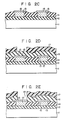
- Fig. 1 illustrates an example of the conventional semiconductor device provided with a 2-layer interconnection.
- Reference numeral 1 denotes a silicon substrate on which a semiconductor element is formed.
- a first aluminium interconnection 3 is formed on said substrate with a SiO 2 layer 2 interposed therebetween. Then, said first aluminium interconnection 3 is covered with a SiO 2 layer 4. After a hole for connecting interconnections with each other is formed in said SiO 2 layer 4, a second aluminium interconnection 5 is formed thereon.
- the conventional semiconductor-manufacturing device however is accompanied with the drawbacks that if the mismatching of a mask takes place in selectively etching the hole in the 5i0 2 layer, said hole will be displaced from its prescribed position in the first aluminium interconnection 3; a narrow groove 6 resulting from overetching appears at the end portion of the hole of the first aluminium interconnection 3; the second aluminium interconnection 5 tends to be broken at said narrow groove 6; to avoid the disconnection of the interconnection, it is necessary to apply an interconnection wider than the hole in consideration of the mismatching of a mask pattern facing the hole; and the broadening of the interconnection will present difficulties in elevating the integration degree of semiconductor elements.
- this invention provides a method of forming a multilayer interconnection for a semiconductor device which comprises the steps of:
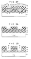
- Figs. 2A to 2F are sectional views showing the sequential steps of forming multilayer interconnection for a semiconductor device according to a first embodiment of this invention.
- a first insulation layer prepared from, for example, a silicon oxide layer 12 is deposited by vapor phase growth on a silicon substrate 11 in which a semiconductor element (not shown) is previously formed. Thereafter, holes facing the semiconductor element are formed.
- First interconnections 13 are formed to cover said holes and silicon oxide layer 12.
- the first interconnection 13 is obtained by first depositing an aluminium layer with a thickness of less than 0.8 microns by, for example, magnetron sputtering, forming an etching mask on said aluminium layer and patterning said etching mask by the reactive ion etching process (RIE) involving the application of a gaseous mixture .consisting of, for example, CCI4and Cl 2 . Thereafter, a silicon oxide layer 14 is formed with a thickness of less than 0.8 microns at a temperature of less than 300°C by the plasma gas phase growth process involving the application of a gaseous mixture consisting of, for example, SiH 4 and N 2 0.
- RIE reactive ion etching process
- the aforementioned silicon oxide layer 1 4 is flattened by the insulation layer-flattening process (U.S. Patent No. 4,377,438) previously proposed by the present inventors which involves the application of the RIE process.
- This insulation layer-flattening process comprises the steps of depositing a silicon nitride layer with a thickness of about one micron on the silicon oxide layer 14, and etching both silicon oxide layer 14 and said silicon nitride layer by the RIE process involving the application of a gaseous mixture consisting of CF 4 and H 2 (containing-27% of hydrogen).
- a gaseous mixture consisting of CF 4 and H 2 (containing-27% of hydrogen).
- a tungsten layer 15 is deposited with a thickness of less than 0.3 micron only on the exposed surface portions of the first interconnections 13 by the vapor phase growth process involving the application of a gaseous mixture consisting of tungsten hexafluoride and H 2 .
- the deposition of said tungsten layer 15 is carried out under the following conditions:
- the tungsten layer 15 is automatically deposited, as shown in Fig. 2C, with a width (for example, 0.1 to 0.2 micron) slightly broader than that of the first interconnection 13.
- a silicon oxide layer 16 is deposited as a third insulation layer with a thickness of less than 0.8 micron by the plasma vapor phase growth process involving the application of a gaseous mixture consisting of SiH 4 and N 2 as is the case with, for example, the second insulation layer.
- a photoresist 17 is applied on the silicon oxide layer 16 for patterning, thereby providing an etching mask.
- the opening of the mask pattern is originally designed to have the same width as that of the first interconnection 13
- Fig. 2D illustrates the case where the opening of said mask pattern slightly extends outward from the surface of said first interconnection 13 due to the mismatching of the mask pattern.
- the silicon oxide layer is etched at the rate of less than 400 tt/min, whereas the tungsten layer 15 is etched at a far smaller rate of less than 1 0 A/min. Consequently, after the surface of the tungsten layer 15 is exposed, etching is not practically advanced. Even though, the aforesaid mask pattern opening somewhat extends outward from the surface of the first interconnection 13, the presence of the proader tungsten layer 15 causes the hole 19 to be formed only in said tungsten layer 15, as shown in Fig. 2E. Therefore, a narrow deep groove 6 is not formed as shown in Fig. 1 representing the conventional method of forming multilayer interconnection for a semiconductor device.
- a second interconnection is formed as shown in Fig. 2F.
- This second interconnection 18 is constructed by the steps of depositing an aluminium layer with a thickness of less than 1 micron by, for example, the magnetron sputtering process, providing an etching mask in said aluminium layer and patterning said etching mask by the RIE process involving the application of a gaseous mixture consisting of, for example, CCl 4 and Cl 2 .
- the second interconnection 18 formed as described above very effectively covers the connection port 19 facing the first interconnection 13 , thereby eliminating the breakage or disconnection of these interconnections 13, 18 and elevating the reliability of a semiconductor element.
- the foregoing embodiment refers to the case where the silicon nitride layer was flattened by the RIE process to form a second insulation layer in such a manner that the grooves in the first interconnection were filled up and the upper portion of said first interconnection was exposed.
- any other etching process may be applied for the flattening of said silicon nitride layer.
- the flattening of said silicon nitride layer can be effected, for example, by applying an organic layer prepared from a resist, organosilicate glass or high polymer resin on the whole of an insulation layer, flattening the surface of said insulation layer and etching said surface by such a process as enables both insulation layer and organic layer to be etched substantially at the same rate.
- a second insulation layer from a fluidized high polymer polyimide resin layer or silicon oxide layer deposited by the RF bias sputtering process, etching the whose surface of an insulation layer formed on the flattened portion of said silicon oxide layer, thereby exposing the surface of the first interconnection pattern.
- the aforementioned embodiment refers to the case where the process of forming the first interconnection pattern was carried out by two steps so as to cover both lateral edges of an insulation layer lying in said first interconnection pattern with a width of, for example, 0.1 to 0.2 micron.
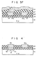
- said process may be performed by a single step. Description may now be made with reference to Figs. 3A to 3F of the single step formation of said first interconnection pattern.
- a SiO 2 layer 22 is deposited by the vapor phase growth process as a first insulation layer with a thickness of 0.7 ⁇ m microns on a silicon substrate 21 on which a semiconductor element is previously formed. Further, a SiO 2 layer 23 is deposited as a second insulation layer with a thickness of 0.8 micron on said first insulation layer 22. Later, a resist mask 24 bearing windows at the regions where said first interconnection is to be formed is deposited by the known PEP process.
- a second insulation layer 23 prepared from SiO 2 is etched by the RIE process involving the application of a gaseous mixture consisting of, for example, CF 4 and H 22 thereby forming a groove or hole 25 along the regions where the first interconnection is to be formed.
- a tungsten layer is embedded in said groove or hole 25 with a greater thickness than the depth thereof (for example, about 1 micron) by the vapor phase growth process involving the application of a gaseous mixture consisting of, for example, WF 6 (tungsten hexafluoride) and H 29 thereby providing first interconnections 26 ,, 26 2 .
- a gaseous mixture consisting of, for example, WF 6 (tungsten hexafluoride) and H 29 thereby providing first interconnections 26 ,, 26 2 .
- the upper portions of the first interconnections 26 1 , 26 2 are formed wider than the corresponding grooves or holes 25 to cover the edges of the SiO 2 layer 23.
- the tungsten layer be deposited under the following conditions:
- the selective growth of the tungsten layer only in the groove or hole 25 of the SiO 2 layer is assumed to arise from the fact that the surface of the bottom of said groove or hole 25 is activated by etching.
- That portion of the substrate 21 which is contacted by the first interconnection 26 1 has a section indicated in, for example, Fig. 4. Namely, before the Si0 2 layer 23 is superposed on the Si0 2 layer 22, a hole 32 is formed in the SiO 2 layer to face the substrate 21, and a tungsten layer 33 is embedded in said hole 32 by the selective vapor phase deposition process. As a result, the first interconnection 26 1 is brought into contact by means of the tungsten layer 33 with a semiconductor element, for example, an n+ diffusion layer 31.
- a semiconductor element for example, an n+ diffusion layer 31.
- an Si0 2 layer 27 is deposited on said first interconnection 26 1 as a third insulation layer with a thickness of about 0.8 micron by the plasma-vapor phase growth process involving the application of a gas mixture consisting of, for example SiH 4 and N 2 .
- a resist mask 28 provided with a window intended for the formation of a hole is deposited by the PEP process on said SiO 2 layer 27.
- the window of said resist mask 28 has the same width as that of the lower portion of the first interconnection 26 1 , namely, the corresponding groove or hole 25.
- Fig. 3D represents the case where the window of the resist mask 28 is slightly displaced from its prescribed position due to the mismatching of its pattern.
- the Si0 2 layer 27 is selectively etched by the RIE process involving the application of a gaseous mixture consisting of, for example, CF and H 21 thereby forming a connection port 29 facing the first interconnection 26. Said etching is performed; for example, under the following conditions:
- the S10 2 layer 27 is etched at the rate of less than 400 A/min, whereas the first interconnection 26 formed of the tungsten layer is etched at a slow rate of less than 10 A/min. If, therefore, the etching is carried out under the above-mentioned condition, practically no progress appears in the etching after the surface of the first interconnection 26 is exposed. Even if the resist opening slightly extends outward from the surface of the first interconnection 26, the hole 29 is formed only on the first interconnection 26 1 as shown in Fig. 3E, because the head portion of said first interconnection 26, is made sufficiently broad to cover both edges of the SiO 2 layer to a slight extent (for example, 0.1 to 0.2 micron). Consequently, a narrow deep groove 6 shown in Fig. 1 repressing the conventional multilayer wiring-manufacturing method for a semiconductor device is not produced.
- a second interconnection 30 is formed to be brought into contact with the first interconnection 26 1 by means of the hole 29 an indicated in Fig. 3F.
- Said second interconnection 30 is formed by first depositing an aluminium interconnection with a thickness of about 1 micron, for example, by the magnetron sputtering process and patterning said aluminium interconnection 30 by the RIE process involving the application of a gas mixture consisting of, for example, CCl 4 and Cl 2 .
- the second interconnection 30 formed as described above very effectively covers the hole 29 formed to face the first interconnection 26 1 .
- the present invention prevents a narrow deep groove from being formed due to overetching as was observed in the conventional method of forming multilayer interconnection for a semiconductor device. Consequently, the breakage or disconnection of the second wire 30 is reliably avoided, thereby noticeably elevating the reliability of a semiconductor device provided with multilayer interconnection.
- the groove or hole 25 shown in Fig. 3B was etched by the RIE process, and simultaneously the bottom surface of said groove or hole 25 was activated.
- This activation desired for the subsequent selective vapor phase growth of the tungsten layer 33 may be carried out by any other process, for example, sputtering, chemical dry etching (CDE) or wet etching involving the application of an acid or base. Said activation may be performed independently of etching, namely, by irradiation of electrons or laser beams.
- the foregoing examples described with reference to Figs. 2 and 3 refer to the case where the first wire was formed by the vapor phase growth of a tungsten layer by application of a gas mixture of WF 6 . However, it is possible to apply another gas mixture of WC!6. Further, it is possible to prepare the first wire by the vapor phase growth of the fluoride or chloride of any other high melting metal such as molybdenum (Mo), niobium (Nb), tantalum (Ta) or titanium (Ti).
- Mo molybdenum
- Nb niobium
- Ta tantalum
- Ti titanium
- the first or second interconnection was formed by depositing an aluminium layer by sputtering.
- the first or second interconnection may be formed by depositing a layer of molybdenum, tungsten, platinum or silicide thereof similarly by sputtering. It will be noted that this invention is effectively applicable also when the first or second interconnection is formed by a laminated layer of the above-mentioned metals or silicides thereof.
Applications Claiming Priority (2)
| Application Number | Priority Date | Filing Date | Title |
|---|---|---|---|
| JP246316/83 | 1983-12-27 | ||
| JP58246316A JPS60138940A (ja) | 1983-12-27 | 1983-12-27 | 半導体装置の製造方法 |
Publications (3)
| Publication Number | Publication Date |
|---|---|
| EP0147203A2 true EP0147203A2 (de) | 1985-07-03 |
| EP0147203A3 EP0147203A3 (en) | 1986-06-25 |
| EP0147203B1 EP0147203B1 (de) | 1989-03-08 |
Family
ID=17146738
Family Applications (1)
| Application Number | Title | Priority Date | Filing Date |
|---|---|---|---|
| EP84308994A Expired EP0147203B1 (de) | 1983-12-27 | 1984-12-20 | Verfahren zum Herstellen von Mehrschichtverbindungen für eine Halbleiteranordnung |
Country Status (4)
| Country | Link |
|---|---|
| US (1) | US4670967A (de) |
| EP (1) | EP0147203B1 (de) |
| JP (1) | JPS60138940A (de) |
| DE (1) | DE3477098D1 (de) |
Cited By (7)
| Publication number | Priority date | Publication date | Assignee | Title |
|---|---|---|---|---|
| FR2588417A1 (fr) * | 1985-10-03 | 1987-04-10 | Bull Sa | Procede de formation d'un reseau metallique multicouche d'interconnexion des composants d'un circuit integre de haute densite et circuit integre en resultant |
| FR2588418A1 (fr) * | 1985-10-03 | 1987-04-10 | Bull Sa | Procede de formation d'un reseau metallique multicouche d'interconnexion des composants d'un circuit integre de haute densite et circuit integre en resultant |
| EP0220517A2 (de) * | 1985-09-30 | 1987-05-06 | Kabushiki Kaisha Toshiba | Halbleiteranordnung mit einem Kontaktfleck |
| EP0234407A1 (de) * | 1986-02-28 | 1987-09-02 | General Electric Company | Verfahren zum Auffüllen von Verbindungs- oder Kontaktlöchern in einer mehrlagigen VLSI-Metallisierungsstruktur |
| EP0407933A2 (de) * | 1989-07-10 | 1991-01-16 | Nec Corporation | In Harz versiegelte Halbleitervorrichtung mit verbessertern Widerstand gegen thermische Spannungen |
| US5587339A (en) * | 1992-09-11 | 1996-12-24 | Sgs-Thomson Microelectronics Ltd. | Method of forming contacts in vias formed over interconnect layers |
| US5874360A (en) * | 1992-09-11 | 1999-02-23 | Sgs-Thomson Microelectronics Limited | Manufacture of semiconductor devices |
Families Citing this family (19)
| Publication number | Priority date | Publication date | Assignee | Title |
|---|---|---|---|---|
| JPS6231116A (ja) * | 1985-08-02 | 1987-02-10 | Toshiba Corp | 半導体装置の製造方法 |
| US4789648A (en) * | 1985-10-28 | 1988-12-06 | International Business Machines Corporation | Method for producing coplanar multi-level metal/insulator films on a substrate and for forming patterned conductive lines simultaneously with stud vias |
| US4963512A (en) * | 1986-03-25 | 1990-10-16 | Hitachi, Ltd. | Method for forming conductor layers and method for fabricating multilayer substrates |
| US4966865A (en) * | 1987-02-05 | 1990-10-30 | Texas Instruments Incorporated | Method for planarization of a semiconductor device prior to metallization |
| US4795722A (en) * | 1987-02-05 | 1989-01-03 | Texas Instruments Incorporated | Method for planarization of a semiconductor device prior to metallization |
| US4789885A (en) * | 1987-02-10 | 1988-12-06 | Texas Instruments Incorporated | Self-aligned silicide in a polysilicon self-aligned bipolar transistor |
| US4948755A (en) * | 1987-10-08 | 1990-08-14 | Standard Microsystems Corporation | Method of manufacturing self-aligned conformal metallization of semiconductor wafer by selective metal deposition |
| US5055423A (en) * | 1987-12-28 | 1991-10-08 | Texas Instruments Incorporated | Planarized selective tungsten metallization system |
| GB2214709A (en) * | 1988-01-20 | 1989-09-06 | Philips Nv | A method of enabling connection to a substructure forming part of an electronic device |
| US5164339A (en) * | 1988-09-30 | 1992-11-17 | Siemens-Bendix Automotive Electronics L.P. | Fabrication of oxynitride frontside microstructures |
| EP0370775B1 (de) * | 1988-11-21 | 1996-06-12 | Kabushiki Kaisha Toshiba | Verfahren zum Herstellen eines Halbleiterbauelementes |
| JP3093429B2 (ja) * | 1992-04-28 | 2000-10-03 | 日本電気株式会社 | 半導体装置の製造方法 |
| JPH10107140A (ja) * | 1996-09-26 | 1998-04-24 | Nec Corp | 多層配線半導体装置とその製造方法 |
| US6433428B1 (en) | 1998-05-29 | 2002-08-13 | Kabushiki Kaisha Toshiba | Semiconductor device with a dual damascene type via contact structure and method for the manufacture of same |
| US6501934B1 (en) | 2000-10-26 | 2002-12-31 | Xerox Corporation | Transfer/transfuse member having increased durability |
| KR100602131B1 (ko) * | 2004-12-30 | 2006-07-19 | 동부일렉트로닉스 주식회사 | 반도체 소자 및 그의 제조방법 |
| JP2007013218A (ja) * | 2006-10-18 | 2007-01-18 | Sony Corp | 半導体装置における配線構造及び配線形成方法 |
| US7735952B2 (en) * | 2007-04-12 | 2010-06-15 | Lexmark International, Inc. | Method of bonding a micro-fluid ejection head to a support substrate |
| IT1401746B1 (it) * | 2010-07-30 | 2013-08-02 | St Microelectronics Srl | Attuatore elettromagnetico integrato, in particolare micro-pompa elettromagnetica per un dispositivo microfluidico basato su tecnologia mems, e relativo procedimento di fabbricazione |
Citations (10)
| Publication number | Priority date | Publication date | Assignee | Title |
|---|---|---|---|---|
| US4005455A (en) * | 1974-08-21 | 1977-01-25 | Intel Corporation | Corrosive resistant semiconductor interconnect pad |
| US4164461A (en) * | 1977-01-03 | 1979-08-14 | Raytheon Company | Semiconductor integrated circuit structures and manufacturing methods |
| EP0021818A1 (de) * | 1979-06-21 | 1981-01-07 | Fujitsu Limited | Elektronische Vorrichtung mit einer Mehrschicht-Bedrahtungsstruktur |
| EP0021133A2 (de) * | 1979-06-06 | 1981-01-07 | Kabushiki Kaisha Toshiba | Halbleitervorrichtung mit einer Leiterbahnelektrode und Verfahren zu deren Herstellung |
| JPS56125857A (en) * | 1980-03-07 | 1981-10-02 | Fujitsu Ltd | Manufacture of semiconductor device |
| EP0046525A2 (de) * | 1980-08-18 | 1982-03-03 | International Business Machines Corporation | Planar mehrlagige Metallisolationsstruktur mit einem Substrat, einem leitenden Verbindungsmuster und einer überlagerten Leiterstruktur und ein Verfahren zum Formen einer solchen Struktur |
| EP0049400A1 (de) * | 1980-09-22 | 1982-04-14 | Kabushiki Kaisha Toshiba | Verfahren zum Glätten einer isolierenden Schicht auf einem Halbleiterkörper |
| GB2119166A (en) * | 1982-04-19 | 1983-11-09 | Mitel Corp | Integrated circuit planarizing process |
| EP0097918A1 (de) * | 1982-06-25 | 1984-01-11 | Matsushita Electronics Corporation | Halbleiteranordnung und Verfahren zu ihrer Herstellung |
| FR2533750A1 (fr) * | 1982-09-24 | 1984-03-30 | Hitachi Ltd | Dispositif electronique, notamment dispositif a circuits integres a semiconducteurs |
Family Cites Families (14)
| Publication number | Priority date | Publication date | Assignee | Title |
|---|---|---|---|---|
| US3366519A (en) * | 1964-01-20 | 1968-01-30 | Texas Instruments Inc | Process for manufacturing multilayer film circuits |
| US3801365A (en) * | 1971-08-05 | 1974-04-02 | Energy Conversion Devices Inc | Method for producing an electrical device |
| JPS51842A (ja) * | 1974-06-21 | 1976-01-07 | Fujitsu Ltd | Mojihyojikiko |
| NL7412383A (nl) * | 1974-09-19 | 1976-03-23 | Philips Nv | Werkwijze voor het vervaardigen van een in- richting met een geleiderpatroon. |
| US4293637A (en) * | 1977-05-31 | 1981-10-06 | Matsushita Electric Industrial Co., Ltd. | Method of making metal electrode of semiconductor device |
| US4272561A (en) * | 1979-05-29 | 1981-06-09 | International Business Machines Corporation | Hybrid process for SBD metallurgies |
| JPS5776833A (en) * | 1980-09-04 | 1982-05-14 | Applied Materials Inc | Heat resistant metal depositing method and product thereof |
| US4330931A (en) * | 1981-02-03 | 1982-05-25 | Intel Corporation | Process for forming metal plated regions and lines in MOS circuits |
| US4441247A (en) * | 1981-06-29 | 1984-04-10 | Intel Corporation | Method of making MOS device by forming self-aligned polysilicon and tungsten composite gate |
| US4476157A (en) * | 1981-07-29 | 1984-10-09 | Tokyo Shibaura Denki Kabushiki Kaisha | Method for manufacturing schottky barrier diode |
| DE3132809A1 (de) * | 1981-08-19 | 1983-03-10 | Siemens AG, 1000 Berlin und 8000 München | Verfahren zum herstellen von integrierten mos-feldeffekttransistoren, insbesondere von komplementaeren mos-feldeffekttransistorenschaltungen mit einer aus metallsiliziden bestehenden zusaetzlichen leiterbahnebene |
| DE3211761A1 (de) * | 1982-03-30 | 1983-10-06 | Siemens Ag | Verfahren zum herstellen von integrierten mos-feldeffekttransistorschaltungen in siliziumgate-technologie mit silizid beschichteten diffusionsgebieten als niederohmige leiterbahnen |
| JPS5982746A (ja) * | 1982-11-04 | 1984-05-12 | Toshiba Corp | 半導体装置の電極配線方法 |
| US4523372A (en) * | 1984-05-07 | 1985-06-18 | Motorola, Inc. | Process for fabricating semiconductor device |
-
1983
- 1983-12-27 JP JP58246316A patent/JPS60138940A/ja active Pending
-
1984
- 1984-12-20 EP EP84308994A patent/EP0147203B1/de not_active Expired
- 1984-12-20 DE DE8484308994T patent/DE3477098D1/de not_active Expired
- 1984-12-24 US US06/685,836 patent/US4670967A/en not_active Expired - Lifetime
Patent Citations (10)
| Publication number | Priority date | Publication date | Assignee | Title |
|---|---|---|---|---|
| US4005455A (en) * | 1974-08-21 | 1977-01-25 | Intel Corporation | Corrosive resistant semiconductor interconnect pad |
| US4164461A (en) * | 1977-01-03 | 1979-08-14 | Raytheon Company | Semiconductor integrated circuit structures and manufacturing methods |
| EP0021133A2 (de) * | 1979-06-06 | 1981-01-07 | Kabushiki Kaisha Toshiba | Halbleitervorrichtung mit einer Leiterbahnelektrode und Verfahren zu deren Herstellung |
| EP0021818A1 (de) * | 1979-06-21 | 1981-01-07 | Fujitsu Limited | Elektronische Vorrichtung mit einer Mehrschicht-Bedrahtungsstruktur |
| JPS56125857A (en) * | 1980-03-07 | 1981-10-02 | Fujitsu Ltd | Manufacture of semiconductor device |
| EP0046525A2 (de) * | 1980-08-18 | 1982-03-03 | International Business Machines Corporation | Planar mehrlagige Metallisolationsstruktur mit einem Substrat, einem leitenden Verbindungsmuster und einer überlagerten Leiterstruktur und ein Verfahren zum Formen einer solchen Struktur |
| EP0049400A1 (de) * | 1980-09-22 | 1982-04-14 | Kabushiki Kaisha Toshiba | Verfahren zum Glätten einer isolierenden Schicht auf einem Halbleiterkörper |
| GB2119166A (en) * | 1982-04-19 | 1983-11-09 | Mitel Corp | Integrated circuit planarizing process |
| EP0097918A1 (de) * | 1982-06-25 | 1984-01-11 | Matsushita Electronics Corporation | Halbleiteranordnung und Verfahren zu ihrer Herstellung |
| FR2533750A1 (fr) * | 1982-09-24 | 1984-03-30 | Hitachi Ltd | Dispositif electronique, notamment dispositif a circuits integres a semiconducteurs |
Non-Patent Citations (1)
| Title |
|---|
| PATENTS ABSTRACTS OF JAPAN, vol. 5, no. 205 (E-88) [877], 25th December 1981; & JP - A - 56 125 857 (FUJITSU K.K.) 02-10-1981 * |
Cited By (13)
| Publication number | Priority date | Publication date | Assignee | Title |
|---|---|---|---|---|
| EP0220517A2 (de) * | 1985-09-30 | 1987-05-06 | Kabushiki Kaisha Toshiba | Halbleiteranordnung mit einem Kontaktfleck |
| EP0220517A3 (en) * | 1985-09-30 | 1987-09-02 | Kabushiki Kaisha Toshiba | Semiconductor device having a contact area |
| US4906592A (en) * | 1985-10-03 | 1990-03-06 | Bull S.A. | Method for forming a multilayered metal network for bonding components of a high-density integrated circuit using a spin on glass layer |
| FR2588418A1 (fr) * | 1985-10-03 | 1987-04-10 | Bull Sa | Procede de formation d'un reseau metallique multicouche d'interconnexion des composants d'un circuit integre de haute densite et circuit integre en resultant |
| EP0221798A1 (de) * | 1985-10-03 | 1987-05-13 | Bull S.A. | Verfahren zum Herstellen eines metallischen Verbindungsmusters für hochintegrierte Schaltungsbauelemente |
| EP0223637A1 (de) * | 1985-10-03 | 1987-05-27 | Bull S.A. | Verfahren zum Herstellen eines metallischen Mehrschicht-Verbindungsmusters für hochintegrierte Schaltungsbauelemente |
| FR2588417A1 (fr) * | 1985-10-03 | 1987-04-10 | Bull Sa | Procede de formation d'un reseau metallique multicouche d'interconnexion des composants d'un circuit integre de haute densite et circuit integre en resultant |
| US4826786A (en) * | 1985-10-03 | 1989-05-02 | Bull, S.A. | Method for forming a multilayered metal network for bonding components of a high-density integrated circuit, and integrated circuit produced thereby |
| EP0234407A1 (de) * | 1986-02-28 | 1987-09-02 | General Electric Company | Verfahren zum Auffüllen von Verbindungs- oder Kontaktlöchern in einer mehrlagigen VLSI-Metallisierungsstruktur |
| EP0407933A2 (de) * | 1989-07-10 | 1991-01-16 | Nec Corporation | In Harz versiegelte Halbleitervorrichtung mit verbessertern Widerstand gegen thermische Spannungen |
| EP0407933A3 (en) * | 1989-07-10 | 1991-07-31 | Nec Corporation | Resin sealed semiconductor device with improved thermal stress resistance |
| US5587339A (en) * | 1992-09-11 | 1996-12-24 | Sgs-Thomson Microelectronics Ltd. | Method of forming contacts in vias formed over interconnect layers |
| US5874360A (en) * | 1992-09-11 | 1999-02-23 | Sgs-Thomson Microelectronics Limited | Manufacture of semiconductor devices |
Also Published As
| Publication number | Publication date |
|---|---|
| EP0147203B1 (de) | 1989-03-08 |
| EP0147203A3 (en) | 1986-06-25 |
| JPS60138940A (ja) | 1985-07-23 |
| US4670967A (en) | 1987-06-09 |
| DE3477098D1 (en) | 1989-04-13 |
Similar Documents
| Publication | Publication Date | Title |
|---|---|---|
| EP0147203B1 (de) | Verfahren zum Herstellen von Mehrschichtverbindungen für eine Halbleiteranordnung | |
| US5595937A (en) | Method for fabricating semiconductor device with interconnections buried in trenches | |
| US4862243A (en) | Scalable fuse link element | |
| EP0127020B1 (de) | Verfahren zum Herstellen einer Mehrschicht-Halbleiteranordnung | |
| US5017510A (en) | Method of making a scalable fuse link element | |
| JPH0754809B2 (ja) | 集積回路の接点孔への相互接続線の自動位置決め方法 | |
| JPH02276232A (ja) | 半導体装置の製造方法 | |
| JPH0215632A (ja) | 半導体集積回路の製造方法 | |
| US5543360A (en) | Method of making a semiconductor device with sidewall etch stopper and wide through-hole having multilayered wiring structure | |
| KR100215847B1 (ko) | 반도체 장치의 금속 배선 및 그의 형성 방법 | |
| JPH01503021A (ja) | シリコンウエハ内に貫通導体を形成する為の平担化方法 | |
| KR20000035246A (ko) | 반도체 구조물의 제조 방법 | |
| KR100221656B1 (ko) | 배선 형성 방법 | |
| JPH09511875A (ja) | 絶縁層上にメタライゼーション層を設け同一マスクを使用して貫通孔を開ける方法 | |
| JP2000195867A (ja) | 象嵌技法を利用した微細金属パタ―ン形成方法 | |
| JPH05299397A (ja) | 金属プラグの形成方法 | |
| EP0191981B1 (de) | Mehrschichtschaltung | |
| JP2805840B2 (ja) | 半導体装置及びその多層配線形成方法 | |
| JPH09275136A (ja) | 半導体装置及びその製造方法 | |
| JP2727587B2 (ja) | 多層配線法 | |
| JP2009054879A (ja) | 集積回路の製造方法 | |
| JPH0334855B2 (de) | ||
| KR100505567B1 (ko) | 반도체장치의리던던시셀과그제조방법 | |
| US20030067078A1 (en) | Semiconductor device and method of manufacturing the same | |
| JPH08330251A (ja) | 半導体装置の製造方法 |
Legal Events
| Date | Code | Title | Description |
|---|---|---|---|
| PUAI | Public reference made under article 153(3) epc to a published international application that has entered the european phase |
Free format text: ORIGINAL CODE: 0009012 |
|
| 17P | Request for examination filed |
Effective date: 19850102 |
|
| AK | Designated contracting states |
Designated state(s): DE FR GB |
|
| PUAL | Search report despatched |
Free format text: ORIGINAL CODE: 0009013 |
|
| AK | Designated contracting states |
Kind code of ref document: A3 Designated state(s): DE FR GB |
|
| 17Q | First examination report despatched |
Effective date: 19871009 |
|
| GRAA | (expected) grant |
Free format text: ORIGINAL CODE: 0009210 |
|
| AK | Designated contracting states |
Kind code of ref document: B1 Designated state(s): DE FR GB |
|
| REF | Corresponds to: |
Ref document number: 3477098 Country of ref document: DE Date of ref document: 19890413 |
|
| ET | Fr: translation filed | ||
| PLBE | No opposition filed within time limit |
Free format text: ORIGINAL CODE: 0009261 |
|
| STAA | Information on the status of an ep patent application or granted ep patent |
Free format text: STATUS: NO OPPOSITION FILED WITHIN TIME LIMIT |
|
| 26N | No opposition filed | ||
| PGFP | Annual fee paid to national office [announced via postgrant information from national office to epo] |
Ref country code: FR Payment date: 19971209 Year of fee payment: 14 |
|
| PGFP | Annual fee paid to national office [announced via postgrant information from national office to epo] |
Ref country code: GB Payment date: 19971211 Year of fee payment: 14 |
|
| PGFP | Annual fee paid to national office [announced via postgrant information from national office to epo] |
Ref country code: DE Payment date: 19971230 Year of fee payment: 14 |
|
| PG25 | Lapsed in a contracting state [announced via postgrant information from national office to epo] |
Ref country code: GB Free format text: LAPSE BECAUSE OF NON-PAYMENT OF DUE FEES Effective date: 19981220 |
|
| GBPC | Gb: european patent ceased through non-payment of renewal fee |
Effective date: 19981220 |
|
| PG25 | Lapsed in a contracting state [announced via postgrant information from national office to epo] |
Ref country code: FR Free format text: LAPSE BECAUSE OF NON-PAYMENT OF DUE FEES Effective date: 19990831 |
|
| REG | Reference to a national code |
Ref country code: FR Ref legal event code: ST |
|
| PG25 | Lapsed in a contracting state [announced via postgrant information from national office to epo] |
Ref country code: DE Free format text: LAPSE BECAUSE OF NON-PAYMENT OF DUE FEES Effective date: 19991001 |