EP0137409A2 - Dispositif de dissolution de films minces semi-conducteurs - Google Patents
Dispositif de dissolution de films minces semi-conducteurs Download PDFInfo
- Publication number
- EP0137409A2 EP0137409A2 EP84111472A EP84111472A EP0137409A2 EP 0137409 A2 EP0137409 A2 EP 0137409A2 EP 84111472 A EP84111472 A EP 84111472A EP 84111472 A EP84111472 A EP 84111472A EP 0137409 A2 EP0137409 A2 EP 0137409A2
- Authority
- EP
- European Patent Office
- Prior art keywords
- resolution
- semiconductor
- films
- resolution device
- semiconductor films
- Prior art date
- Legal status (The legal status is an assumption and is not a legal conclusion. Google has not performed a legal analysis and makes no representation as to the accuracy of the status listed.)
- Granted
Links
Images
Classifications
-
- G—PHYSICS
- G01—MEASURING; TESTING
- G01N—INVESTIGATING OR ANALYSING MATERIALS BY DETERMINING THEIR CHEMICAL OR PHYSICAL PROPERTIES
- G01N21/00—Investigating or analysing materials by the use of optical means, i.e. using sub-millimetre waves, infrared, visible or ultraviolet light
- G01N21/62—Systems in which the material investigated is excited whereby it emits light or causes a change in wavelength of the incident light
- G01N21/71—Systems in which the material investigated is excited whereby it emits light or causes a change in wavelength of the incident light thermally excited
- G01N21/74—Systems in which the material investigated is excited whereby it emits light or causes a change in wavelength of the incident light thermally excited using flameless atomising, e.g. graphite furnaces
-
- G—PHYSICS
- G01—MEASURING; TESTING
- G01N—INVESTIGATING OR ANALYSING MATERIALS BY DETERMINING THEIR CHEMICAL OR PHYSICAL PROPERTIES
- G01N1/00—Sampling; Preparing specimens for investigation
- G01N1/28—Preparing specimens for investigation including physical details of (bio-)chemical methods covered elsewhere, e.g. G01N33/50, C12Q
- G01N1/40—Concentrating samples
- G01N1/4044—Concentrating samples by chemical techniques; Digestion; Chemical decomposition
-
- H—ELECTRICITY
- H01—ELECTRIC ELEMENTS
- H01L—SEMICONDUCTOR DEVICES NOT COVERED BY CLASS H10
- H01L22/00—Testing or measuring during manufacture or treatment; Reliability measurements, i.e. testing of parts without further processing to modify the parts as such; Structural arrangements therefor
- H01L22/10—Measuring as part of the manufacturing process
- H01L22/12—Measuring as part of the manufacturing process for structural parameters, e.g. thickness, line width, refractive index, temperature, warp, bond strength, defects, optical inspection, electrical measurement of structural dimensions, metallurgic measurement of diffusions
Definitions
- the present invention relates to a resolution device for semiconductor thin films, more particular, to semiconductor thin film (resolution device) for preparating samples, that are scarcely contaminated by the decomposition reagents or the surroundings, to be used in analyzing ultratrace amounts of impurities in semiconductor thin films.
- Semiconductor films such as Sio 2 film or Si 3 N 4 film have been used as a partial diffusion masking for doping reagent or a protective film for sputtered metallic films in silicon semiconductor.
- impurities like Na, K, or Fe
- the flameless atomic absorption spectrophotometer For measuring impurities in semiconductor films, the flameless atomic absorption spectrophotometer has been used in the past. Measurements are taken by placing the semiconductor film samples for flameless atomic absorption spectrophotometry on the flameless atomic absorption spectrophotometer. However, these exists a serious problem in the preparation of samples for the spectrophotometry.
- a semiconductor film is soaked into the mixture of hydrofluoric acid and sulfuric acid, and after direct decomposition, the dissolved solution obtained is evaporated and dried to obtain the residues.
- Samples for flameless atomic absorption spectroanlysis are obtained by diluting the residues to a predetermined volume with pure water.
- contamination by the reagent used for resolving the semiconductor sample is exceedingly large.
- these reagents already contain impurities (Na, K, and the like) in excess of 0.1 ppb so that it has been extremely difficult to accurately measure the amount of impurities in a semiconductor film of less than 10 -10 g/cm 2 by means of flameless atomic absorption spectrophotometer.
- An object of the present invention is to provide a semiconductor film resolution device which is capable of preparing semiconductor film samples for flameless atomic- absorption spectrophotometry that are scarcely contaminated by the resolution reagents or by the surroundings.
- Another object of the present invention is to provide a semiconductor-film resolution device which is capable of preparing semiconductor film samples of which the flameless atomic absorption spectrophotometer can measure the impurity amount with high sensitivity.
- Still other object of the present invention is to provide a resolution device which is capable of preparing semiconductor film samples by a simple operation.
- an improved semiconductor film resolution device which includes a sealed container, a container installed within the sealed container for storing hydrofluoric acid to be used for generating hydrogen, fluoride gas, means installed within the sealed container holding semiconductor films, and a receptacle installed at the bottom of the sealed container for receiving the resolved solution of the semiconductor films.
- the semiconductor films that are held by the holding means are resolved by hydrogen fluoride gas with low impurity content generated at the storage container of hydrofluoric acid.
- the resolved solution is collected in the receptacle for resolved solution, and is supplied directly to a flameless atomic absorption spectrophotometer.
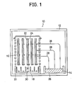
- This semiconductor film resolution device includes a sealed container 12, a hydrofluoric acid storage container 14, such as a beaker for evaporating hydrogen fluoride gas, a film supporter 16 such as a wafer carrier, and a resolved solution receptacle 18, a receiving tray.
- the material for all parts of the device is teflon, and the device is cleaned by heating in mixed solution of hydrofluoric acid, nitric acid, and hydrochloric acid and is washed away.with pure water prior to its use.
- the sample wafers 22 with Si0 2 or Si 3 N 4 films 24 are leaned against the wafer carrier 16, hydrofluoric acid 26 is poured into the evaporation beaker 14, and the entire device is left standing for a predetermined duration of time. Little effect has been observed in the sensitivity and accuracy of analysis even if the device is left standing until 300 minutes after the completion of resolution.
- the temperature at which it is to be left is desirable to be in the range of 20 to 35°C.
- Semiconductor films 24 are resolved completely by the hydrogen fluoride gas 28 that was generated from the beaker 14, and most of the resolved solution drops 30 into the resolved solution receptacle 18.
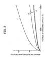
- the rate of resolution varied with the type and thickness of the film 24.
- the time required for resolution in the case of fluoric acid (50%) of 100 ml, temperature of 30 o C, spatial volume of the sealed container of about 16,000 cm 3 , and film thickness of 10,000 A, as shown in Fig. 2, are 31 minutes for thermally oxidized SiO 2 films C, 29 minutes for LPCVD-Si0 2 films D, 47 minutes for plasma CVD-Si 3 N 4 films B, and 108 minutes for LPCVD-Si 3 N 4 films A.
- the resolved solution is collected with a micropipette, and following stirring and weighing, is measured directly with a flameless atomic absorption spectrophotometer without carrying out separate concentration by evaporation and drying.
- the resolution treatment according to the present method is carried out with hydrogen fluoride gas without directly acid-resolving the semiconductor films with resolution solution, it becomes possible to achieve detection with an extremely high sensitivity.
- the impurity content of the hydrogen fluoride gas used in the present device is extremely low, since it is the gas that has evaporated out from the hydrofluoric acid solution, even if the solution contains certain amount of impurities. ! Therefore, the impurity content of the solution collected for samples is correspondingly low also. If evaporation is done by heating the hydrofluoric acid solution, then the impurities in the solution tend to evaporate out also, giving rise to a possibility of increasing the impurity content of the hydrogen fluoride gas. This is the reason why it is desirable to have evaporation at the room temperature in the range of 20°C and 35°C.
- the resolution device in the resolution device according to the present invention, samples are decomposed with hydrogen fluoride gas of high purity, rather than directly acid resolving it, so that it is possible to reduce the contamination to a substantial degree.
- the device according to the present invention it becomes possible to accomplish a super-high sensitivity which is 1,000 times as high as for the prior art method, and to analyze metallic impurities, such as Na , K , Fe , and others, of the order of 10-13 g/cm 2 in the films.
- the operation for preparation of resolved solution to be used as samples for analysis is simple so that the industrial significance of the present invention is quite substantial.
- the storage container of hydrofluoric acid which is a part of the device according to the present invention, may be of any make as long as it is capable of storing a predetermined amount of hydrofluoric acid, and evaporating and generating from it hydrogen fluoride gas with high efficiency.
- the means for holding the semiconductor films is a unit which is installed within the sealed container to hold the edges of the semiconductor films to be decomposed, having such a positional relationship as to have the semiconductor films resolved by making a contact with the hydrogen fluoride gas that comes from the storage container.
- the holding means may be made in such a way as to hold just one film sample (for example, a sample wafer with an attached film) or may be made in such a way as to hold a plurality of film samples.
- the material of the components which constitute the device of the present invention may be anything as long as it does not interfere, either directly or indirectly, with precise measurements of impurities in the films to be measured.
- the gas to be used for resolution is hydrogen fluoride
- Teflon not only has excellent acid-proof and heat-proof properties, but also permits an easy removal of impurities by washing with a mixed solution of hydrofluoric acid, nitric acid, hydrochloric acid, and the like.
- the dissolution of impurities from teflon which have undergone such a washing is extremely small so that it is considered to be a material which is suitable for the objects of the present invention.
Applications Claiming Priority (2)
| Application Number | Priority Date | Filing Date | Title |
|---|---|---|---|
| JP58176503A JPH0658927B2 (ja) | 1983-09-26 | 1983-09-26 | 半導体薄膜の分析方法および分析用試料の回収装置 |
| JP176503/83 | 1983-09-26 |
Publications (3)
| Publication Number | Publication Date |
|---|---|
| EP0137409A2 true EP0137409A2 (fr) | 1985-04-17 |
| EP0137409A3 EP0137409A3 (en) | 1986-06-25 |
| EP0137409B1 EP0137409B1 (fr) | 1988-12-14 |
Family
ID=16014776
Family Applications (1)
| Application Number | Title | Priority Date | Filing Date |
|---|---|---|---|
| EP84111472A Expired EP0137409B1 (fr) | 1983-09-26 | 1984-09-26 | Dispositif de dissolution de films minces semi-conducteurs |
Country Status (4)
| Country | Link |
|---|---|
| US (1) | US4584886A (fr) |
| EP (1) | EP0137409B1 (fr) |
| JP (1) | JPH0658927B2 (fr) |
| DE (1) | DE3475653D1 (fr) |
Cited By (3)
| Publication number | Priority date | Publication date | Assignee | Title |
|---|---|---|---|---|
| EP0653623A1 (fr) * | 1993-05-21 | 1995-05-17 | Daikin Industries, Limited | Methode de determination quantitative d'impuretes metalliques a l'etat de traces dans un polymere fluore, et procede de production de polymere fluore faisant appel a ladite methode |
| EP0657924A2 (fr) * | 1993-12-09 | 1995-06-14 | Kabushiki Kaisha Toshiba | Methode pour analyser les impuretés sur un substrat semi-conducteur |
| DE19713090B4 (de) * | 1996-03-28 | 2004-06-17 | Kabushiki Kaisha Toshiba, Kawasaki | Verfahren und Apparatur zum Ätzen von Silicium-Materialien |
Families Citing this family (15)
| Publication number | Priority date | Publication date | Assignee | Title |
|---|---|---|---|---|
| JPS6211129A (ja) * | 1985-07-08 | 1987-01-20 | Toshiba Corp | 半導体薄膜の形成・分解装置 |
| JPS62142843U (fr) * | 1986-03-04 | 1987-09-09 | ||
| JPH08233709A (ja) * | 1988-04-25 | 1996-09-13 | Toshiba Corp | 不純物の測定方法 |
| US4990459A (en) * | 1988-04-25 | 1991-02-05 | Kabushiki Kaisha Toshiba | Impurity measuring method |
| JPH0625717B2 (ja) * | 1988-04-25 | 1994-04-06 | 株式会社東芝 | 不純物の測定方法 |
| US5395446A (en) * | 1988-11-21 | 1995-03-07 | Kabushiki Kaisha Toshiba | Semiconductor treatment apparatus |
| US5014217A (en) * | 1989-02-09 | 1991-05-07 | S C Technology, Inc. | Apparatus and method for automatically identifying chemical species within a plasma reactor environment |
| US5248614A (en) * | 1991-09-12 | 1993-09-28 | Taiwan Semiconductor Manufacturing Company | Thin film sampling method for film composition quantitative analysis |
| JP2537946Y2 (ja) * | 1991-12-28 | 1997-06-04 | 山村商事株式会社 | 自動販売機 |
| US5395482A (en) * | 1992-11-13 | 1995-03-07 | Fuji Photo Film Co., Ltd. | Ultra high purity vapor phase treatment |
| JP2716923B2 (ja) * | 1993-03-26 | 1998-02-18 | 株式会社東芝 | 半導体基板表面吸着有機物の測定方法 |
| JP3051013B2 (ja) * | 1993-12-21 | 2000-06-12 | 株式会社東芝 | 不純物分析方法 |
| US6168961B1 (en) | 1998-05-21 | 2001-01-02 | Memc Electronic Materials, Inc. | Process for the preparation of epitaxial wafers for resistivity measurements |
| WO2015074181A1 (fr) * | 2013-11-19 | 2015-05-28 | 成都市产品质量监督检验院 | Appareil de soufflage de l'azote et procédé de dissolution en voie humide utilisant un appareil soufflant de l'azote |
| CN115433580B (zh) * | 2022-10-27 | 2023-08-18 | 湖北九宁化学科技有限公司 | 一种光电行业蚀刻液的生产方法 |
Citations (2)
| Publication number | Priority date | Publication date | Assignee | Title |
|---|---|---|---|---|
| JPS5726734A (en) * | 1980-07-24 | 1982-02-12 | Toshiba Corp | Analysis of si in gaas |
| JPS58740A (ja) * | 1981-06-26 | 1983-01-05 | Toshiba Corp | ガリウム砒素中の微量元素の定量法 |
Family Cites Families (11)
| Publication number | Priority date | Publication date | Assignee | Title |
|---|---|---|---|---|
| US3824016A (en) * | 1972-06-16 | 1974-07-16 | R Woodriff | Combined sample collection and vaporization system for spectro-chemical analysis |
| US3976377A (en) * | 1975-02-03 | 1976-08-24 | Rca Corporation | Method of obtaining the distribution profile of electrically active ions implanted in a semiconductor |
| JPS5310974A (en) * | 1976-07-17 | 1978-01-31 | Mitsubishi Electric Corp | Etching method of oxide film |
| JPS5950928B2 (ja) * | 1978-02-17 | 1984-12-11 | 松下電器産業株式会社 | フレ−ムレス原子吸光分析法 |
| US4361401A (en) * | 1978-05-22 | 1982-11-30 | Instrumentation Laboratory Inc. | Automatic sample deposition in flameless analysis |
| JPS552982A (en) * | 1978-06-23 | 1980-01-10 | Matsushita Electric Ind Co Ltd | Semi-conductor layer thickness measuring method |
| JPS5560807A (en) * | 1978-11-01 | 1980-05-08 | Chino Works Ltd | Measuring instrument for film |
| JPS5590838A (en) * | 1978-12-28 | 1980-07-09 | Fujitsu Ltd | Method of fabricating sample for use in permeative electron microscope |
| JPS55125632A (en) * | 1979-03-23 | 1980-09-27 | Fujitsu Ltd | Etching |
| JPS5714736A (en) * | 1980-06-30 | 1982-01-26 | Mitsubishi Chem Ind Ltd | Rapid, wet-type sample decomposing device |
| JPS57204432A (en) * | 1981-06-11 | 1982-12-15 | Mitsubishi Heavy Ind Ltd | Testing method for discoloration by gas diffusion |
-
1983
- 1983-09-26 JP JP58176503A patent/JPH0658927B2/ja not_active Expired - Lifetime
-
1984
- 1984-09-25 US US06/654,216 patent/US4584886A/en not_active Expired - Lifetime
- 1984-09-26 EP EP84111472A patent/EP0137409B1/fr not_active Expired
- 1984-09-26 DE DE8484111472T patent/DE3475653D1/de not_active Expired
Patent Citations (2)
| Publication number | Priority date | Publication date | Assignee | Title |
|---|---|---|---|---|
| JPS5726734A (en) * | 1980-07-24 | 1982-02-12 | Toshiba Corp | Analysis of si in gaas |
| JPS58740A (ja) * | 1981-06-26 | 1983-01-05 | Toshiba Corp | ガリウム砒素中の微量元素の定量法 |
Non-Patent Citations (3)
| Title |
|---|
| PATENT ABSTRACTS OF JAPAN, vol. 6, no. 88 (P-118)[966], 26th May 1982; & JP-A-57 026 734 (TOKYO SHIBAURA DENKI) 12-02-1982 * |
| PATENT ABSTRACTS OF JAPAN, vol. 7, no. 70 (P-185)[1215], 23rd March 1983; & JP-A-58 000 740 (TOKYO SHIBAURA DENKI K.K.) 05-01-1983 * |
| TRENDS IN ANALYTICAL CHEMISTRY, vol. 2, no. 5, May 1983, pages 118-121, Cambridge, GB; C. LEA "Preparation of samples for surface analysis" * |
Cited By (6)
| Publication number | Priority date | Publication date | Assignee | Title |
|---|---|---|---|---|
| EP0653623A1 (fr) * | 1993-05-21 | 1995-05-17 | Daikin Industries, Limited | Methode de determination quantitative d'impuretes metalliques a l'etat de traces dans un polymere fluore, et procede de production de polymere fluore faisant appel a ladite methode |
| EP0653623A4 (fr) * | 1993-05-21 | 1997-04-23 | Daikin Ind Ltd | Methode de determination quantitative d'impuretes metalliques a l'etat de traces dans un polymere fluore, et procede de production de polymere fluore faisant appel a ladite methode. |
| EP0657924A2 (fr) * | 1993-12-09 | 1995-06-14 | Kabushiki Kaisha Toshiba | Methode pour analyser les impuretés sur un substrat semi-conducteur |
| EP0657924A3 (fr) * | 1993-12-09 | 1996-07-10 | Toshiba Kk | Methode pour analyser les impuretés sur un substrat semi-conducteur. |
| US5633172A (en) * | 1993-12-09 | 1997-05-27 | Kabushiki Kaisha Toshiba | Method for analying an impurity on a semiconductor substrate |
| DE19713090B4 (de) * | 1996-03-28 | 2004-06-17 | Kabushiki Kaisha Toshiba, Kawasaki | Verfahren und Apparatur zum Ätzen von Silicium-Materialien |
Also Published As
| Publication number | Publication date |
|---|---|
| US4584886A (en) | 1986-04-29 |
| EP0137409A3 (en) | 1986-06-25 |
| DE3475653D1 (en) | 1989-01-19 |
| JPH0658927B2 (ja) | 1994-08-03 |
| EP0137409B1 (fr) | 1988-12-14 |
| JPS6069531A (ja) | 1985-04-20 |
Similar Documents
| Publication | Publication Date | Title |
|---|---|---|
| EP0137409B1 (fr) | Dispositif de dissolution de films minces semi-conducteurs | |
| JP3051023B2 (ja) | 珪素質分析試料中の不純物高精度分析のための処理方法及びその装置 | |
| JP3690484B2 (ja) | シリコン基板表面の金属不純物分析方法 | |
| US5426057A (en) | Method of measuring amount of organic material adsorbed to surface of semiconductor substrate | |
| JP3414976B2 (ja) | 不純物分析試料容器およびそれに用いられる試料収容部材 | |
| Hub et al. | Application of ETV-ICPMS in semiconductor process control | |
| JP3804864B2 (ja) | 不純物の分析方法 | |
| WO2000004579A9 (fr) | Procede de cartographie de la concentration en contaminants metalliques sur la surface d'une plaquette de silicium | |
| JP2004037430A (ja) | イオン濃度測定用イオンセンサーとその製造方法およびそれを用いたイオン濃度測定器 | |
| US6225136B1 (en) | Method of producing a contaminated wafer | |
| Fuchs-Pohl et al. | Determination of silicon traces in process chemicals for semiconductor production by ETAAS | |
| JP2001223251A (ja) | 石英中に含有される金属の分析方法 | |
| JPH01189558A (ja) | Si半導体基板の表面分析方法 | |
| JPH0525068B2 (fr) | ||
| JP3613027B2 (ja) | フッ酸中のアルミニウムの分析方法 | |
| KR100204339B1 (ko) | 반도체 분석장치 및 그 방법 | |
| JPS6138547A (ja) | 試料分解装置及びそれを用いた試料分解方法 | |
| JPS63195540A (ja) | 半導体薄膜の分解装置 | |
| JPS61151444A (ja) | 半導体試料中のリンの分析方法 | |
| KR20000067357A (ko) | 반도체 웨이퍼 표면의 오염 시료를 채취하는 방법 | |
| JPH04110647A (ja) | 半導体薄膜中の超微量元素分析方法 | |
| JPH0357422B2 (fr) | ||
| JPS62841A (ja) | 半導体材料中のホウ素分析方法 | |
| JPH07333116A (ja) | 試料分解装置及び試料分解方法 | |
| JPH034166A (ja) | ウエハ表面の不純物量の測定方法 |
Legal Events
| Date | Code | Title | Description |
|---|---|---|---|
| PUAI | Public reference made under article 153(3) epc to a published international application that has entered the european phase |
Free format text: ORIGINAL CODE: 0009012 |
|
| AK | Designated contracting states |
Designated state(s): DE FR GB |
|
| PUAL | Search report despatched |
Free format text: ORIGINAL CODE: 0009013 |
|
| AK | Designated contracting states |
Kind code of ref document: A3 Designated state(s): DE FR GB |
|
| 17P | Request for examination filed |
Effective date: 19860723 |
|
| 17Q | First examination report despatched |
Effective date: 19880311 |
|
| GRAA | (expected) grant |
Free format text: ORIGINAL CODE: 0009210 |
|
| AK | Designated contracting states |
Kind code of ref document: B1 Designated state(s): DE FR GB |
|
| REF | Corresponds to: |
Ref document number: 3475653 Country of ref document: DE Date of ref document: 19890119 |
|
| ET | Fr: translation filed | ||
| PLBE | No opposition filed within time limit |
Free format text: ORIGINAL CODE: 0009261 |
|
| STAA | Information on the status of an ep patent application or granted ep patent |
Free format text: STATUS: NO OPPOSITION FILED WITHIN TIME LIMIT |
|
| 26N | No opposition filed | ||
| REG | Reference to a national code |
Ref country code: GB Ref legal event code: 746 Effective date: 19980915 |
|
| REG | Reference to a national code |
Ref country code: FR Ref legal event code: D6 |
|
| REG | Reference to a national code |
Ref country code: GB Ref legal event code: IF02 |
|
| PGFP | Annual fee paid to national office [announced via postgrant information from national office to epo] |
Ref country code: FR Payment date: 20030909 Year of fee payment: 20 |
|
| PGFP | Annual fee paid to national office [announced via postgrant information from national office to epo] |
Ref country code: GB Payment date: 20030924 Year of fee payment: 20 |
|
| PGFP | Annual fee paid to national office [announced via postgrant information from national office to epo] |
Ref country code: DE Payment date: 20031009 Year of fee payment: 20 |
|
| PG25 | Lapsed in a contracting state [announced via postgrant information from national office to epo] |
Ref country code: GB Free format text: LAPSE BECAUSE OF EXPIRATION OF PROTECTION Effective date: 20040925 |
|
| REG | Reference to a national code |
Ref country code: GB Ref legal event code: PE20 |