EP0657924A2 - Methode pour analyser les impuretés sur un substrat semi-conducteur - Google Patents
Methode pour analyser les impuretés sur un substrat semi-conducteur Download PDFInfo
- Publication number
- EP0657924A2 EP0657924A2 EP94119316A EP94119316A EP0657924A2 EP 0657924 A2 EP0657924 A2 EP 0657924A2 EP 94119316 A EP94119316 A EP 94119316A EP 94119316 A EP94119316 A EP 94119316A EP 0657924 A2 EP0657924 A2 EP 0657924A2
- Authority
- EP
- European Patent Office
- Prior art keywords
- semiconductor substrate
- impurity
- areas
- droplets
- measured
- Prior art date
- Legal status (The legal status is an assumption and is not a legal conclusion. Google has not performed a legal analysis and makes no representation as to the accuracy of the status listed.)
- Granted
Links
Images

Classifications
-
- H—ELECTRICITY
- H01—ELECTRIC ELEMENTS
- H01L—SEMICONDUCTOR DEVICES NOT COVERED BY CLASS H10
- H01L22/00—Testing or measuring during manufacture or treatment; Reliability measurements, i.e. testing of parts without further processing to modify the parts as such; Structural arrangements therefor
- H01L22/20—Sequence of activities consisting of a plurality of measurements, corrections, marking or sorting steps
-
- H—ELECTRICITY
- H01—ELECTRIC ELEMENTS
- H01L—SEMICONDUCTOR DEVICES NOT COVERED BY CLASS H10
- H01L22/00—Testing or measuring during manufacture or treatment; Reliability measurements, i.e. testing of parts without further processing to modify the parts as such; Structural arrangements therefor
- H01L22/10—Measuring as part of the manufacturing process
- H01L22/12—Measuring as part of the manufacturing process for structural parameters, e.g. thickness, line width, refractive index, temperature, warp, bond strength, defects, optical inspection, electrical measurement of structural dimensions, metallurgic measurement of diffusions
-
- Y—GENERAL TAGGING OF NEW TECHNOLOGICAL DEVELOPMENTS; GENERAL TAGGING OF CROSS-SECTIONAL TECHNOLOGIES SPANNING OVER SEVERAL SECTIONS OF THE IPC; TECHNICAL SUBJECTS COVERED BY FORMER USPC CROSS-REFERENCE ART COLLECTIONS [XRACs] AND DIGESTS
- Y10—TECHNICAL SUBJECTS COVERED BY FORMER USPC
- Y10T—TECHNICAL SUBJECTS COVERED BY FORMER US CLASSIFICATION
- Y10T436/00—Chemistry: analytical and immunological testing
- Y10T436/25—Chemistry: analytical and immunological testing including sample preparation
- Y10T436/25375—Liberation or purification of sample or separation of material from a sample [e.g., filtering, centrifuging, etc.]
Definitions
- the present invention relates to a method for analyzing an impurity present on the surface of a semiconductor substrate and, in particular, to a method for measuring an amount of impurity on a semiconductor substrate surface at those local areas of a repeated pattern.
- a solution for impurity collection such as an acid solution
- a solution for impurity collection is dropped on a whole surface area of a semiconductor substrate or on a nearly liquid-drop-size area on the surface of a semiconductor substrate where an impurity is collected. Then an amount of impurity collected in that solution used is measured by a chemical analytic apparatus such as a flameless atomic absorption apparatus.
- the surface distribution pattern of an impurity concentration depends upon the surface pattern of the semiconductor substrate.
- the device surface pattern has become very small with the microminiaturization of the semiconductor element so that the surface distribution pattern of the impurity concentration becomes very small.
- the surface pattern of the device is of the order of a micron or submicron.
- the surface resolution by the conventional analytical method is of the order of a few cm2, an ordinary size of to-be-collected liquid drops at best, thus failing to achieve high-accurate analysis.
- a method for analyzing an impurity on the surface of a semiconductor substrate comprising the steps of: oxidizing those to-be-measured areas on a surface of a semiconductor substrate to provide corresponding oxide films and trapping an impurity in the oxide film at each area of the semiconductor substrate; removing an impurity from other than the areas on the surface of the semiconductor substrate; dissolving the oxide films on the to-be-measured areas into droplets; collecting the droplets into a drop; and measuring an amount of impurity in the drop.
- a method for analyzing an impurity on a semiconductor substrate comprising the steps of: depositing nitride films on those to-be-measured areas on a surface of a semiconductor substrate and trapping an impurity in the nitride film at each area of the semiconductor substrate; removing an impurity from other than the areas on the surface of the semiconductor substrate; dissolving the nitride films on the to-be-measured areas into droplets; collecting the droplets into a drop; and measuring an amount of impurity in the drop.
- a method for analyzing an impurity on a semiconductor substrate comprising the steps of: oxidizing those to-be-measured areas on a surface of a semiconductor substrate to provide corresponding oxide films and trapping an impurity in the oxide film at each area of the semiconductor substrate; removing an impurity from other than the areas on the surface of the semiconductor substrate; dissolving the oxide films on the to-be-measured areas into droplets; collecting the droplets into a drop; measuring an amount of impurity in the drop; repeating the oxidizing step through the measuring step; and plotting the amount of impurity obtained at each measuring step in a depth direction of the semiconductor substrate.
- a method for analyzing an impurity on a semiconductor substrate comprising the steps of: depositing nitride films on those to-be-measured areas on a surface of a semiconductor substrate and trapping an impurity in the nitride film at each area of the semiconductor substrate; removing an impurity from other than the areas on the surface of the semiconductor substrate; dissolving the nitride films on the to-be-measured areas into droplets; collecting the droplets into a drop; measuring an amount of impurity in the drop; repeating the nitride film depositing step through the measuring step; and plotting the amount of impurity obtained at each measuring step in a depth direction of the semiconductor substrate.
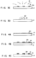
- FIG. 1 shows a model of a surface pattern on a semiconductor silicon substrate.
- a surface pattern layer 14 is formed of, for example, an insulating layer for semiconductor element isolation, providing a repeated pattern.
- Semiconductor element areas 16 are each formed by a semiconductor substrate surface area bounded by the isolation layer 14.
- a respective local area 18 to be measured constitutes a portion of each element area, that is, those local areas 18 constitute mutually corresponding areas on the repeated pattern.
- FIG. 2 is a cross-sectional view, taken along line II-II in FIG. 1.
- the insulating pattern 14 for isolation is omitted for brevity's sake.
- the analytical examination is made by the following way.
- an ultraviolet radiation 22 is directed with a given pattern as a mask to those to-be-measured local areas 18 on the surface of a semiconductor silicon substrate 12 in a clean oxygen atmosphere.
- an insulating layer pattern 14 for isolation is omitted for the sake of simplification.
- the surface of the semiconductor substrate 12 is cleaned with a suitable detergent, such as an acid solution consisting of, for example, a hydrochloric acid/hydrogen peroxide-mixed aqueous solution. As shown in FIG. 3B, an impurity on other than the to-be-treated area on the surface of the semiconductor substrate is removed.
- a suitable detergent such as an acid solution consisting of, for example, a hydrochloric acid/hydrogen peroxide-mixed aqueous solution.
- the resultant semiconductor substrate surface 12 is exposed with, for example, a hydrofluoric acid vapor to dissolve the oxide film 24, so that, as shown in FIG. 3C, very fine droplets (impurity drops) 30 containing the impurity are left on the surface of the substrate 12.
- a hydrofluoric acid vapor to dissolve the oxide film 24, so that, as shown in FIG. 3C, very fine droplets (impurity drops) 30 containing the impurity are left on the surface of the substrate 12.
- the liquid may be water, preferably, a high-purity acid solution consisting of, for example, a hydrochloric acid/hydrogen peroxide aqueous solution.
- an amount of impurity 26a in the gathered drop is measured by a known chemical spectrometer, such as a flameless atomic absorption spectrometer and inductively coupled plasma mass spectrometer. From the measured amount it is possible to calculate the concentration level of the impurity per unit area of the area to be measured. Any other measuring device may be used in place of the chemical spectrometer.
- the present invention it is possible according to the present invention to achieve a high surface resolution and hence to measure, with high accuracy, an amount of impurity 26a in the local areas 18 on the semiconductor substrate 12. In other words it it possible to highly accurately obtain the distribution characteristic from the amount of impurity on the surface of the semiconductor substrate 12.
- the local areas on the substrate surface correspond to a regularly repeated pattern array on the semiconductor surface 12, the present invention is not restricted thereto and it is also possible to measure a single local area 61 or any plurality of local areas.
- the sensitivity of the present method under the chemical analysis is of the order of 109 to 1010 atoms/cm2, a very high value than an ordinary sensitivity under a physical analysis of the order of 1013 to 1014 atoms/cm2. Even the impurity distribution characteristic of a pattern as small as a micron or sub-micron order under the pattern rule of a recent device can be obtained with high accuracy.
- the position of the surface portion of the semiconductor substrate 12 at which the oxide film 24 has been dissolved is lowered in the depth direction of the semiconductor substrate 12. Therefore, after the step of collecting the very fine droplets 30, an insulating film is formed on those local areas, to be measured, on the resultant semiconductor substrate structure by the application of an ultraviolet radiation with the above-mentioned mask again used and, by doing so repetitively, a corresponding distribution characteristic is formed, each time, relative to the amount of impurity, so that amount-of-impurity distribution characteristics can be gained at different positions in a depth direction of the semiconductor structure, that is, it is possible to obtain amount-of-impurity distribution characteristics in the depth of the semiconductor structure by plotting these distribution characteristics in that depth direction.
- the oxide film 24 has been explained as being formed by an irradiation with the ultraviolet radiation and hence application of heat, it may be possible to utilize the exposure and hence heating of, for example, a laser beam.
- the formation of the oxide film 24 is not restricted only to the exposure of light.
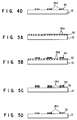
- an SiN film or SiO2 film 42 is formed, by a known chemical vapor deposition method, on the whole surface of a semiconductor silicon substrate 12 as shown in FIG. 4A and a photoresist layer 44 whose pattern is an inverted version of a pattern for those to-be-measured areas on the semiconductor substrate is formed by a known method on the SiO2 film 42 as shown in FIG. 4B.
- the oxide film 42 may be replaced with a nitride film. Forming the nitride film can be achieved in substantially the same way as in the case where the SiO2 film 42 is formed on the substrate as shown in FIGS. 4A to 4D. That is, an SiN film 52 is formed, by a known chemical vapor deposition method, on the whole surface of a semiconductor silicon substrate 12 as shown in FIG. 5A and a photoresist layer 54 whose pattern is an inverted version of a pattern for those to-be-measured areas on a semiconductor substrate 12 is formed, by a known method, on the SiN film 52 as shown in FIG. 5B.
- the surface of the resultant semiconductor structure is selectively etched with a photoresist layer 54 used as a mask to leave only those to-be-measured areas of the SiN film 52 on the surface of the semiconductor device as shown in FIG. 5C, followed by the elimination of the photoresist layer 54 as shown in FIG. 5D.
- the remaining processing steps are the same as those using the SiO2 film set out in conjunction with FIGS. 3A to 3D.
Landscapes
- Engineering & Computer Science (AREA)
- Manufacturing & Machinery (AREA)
- Computer Hardware Design (AREA)
- Microelectronics & Electronic Packaging (AREA)
- Power Engineering (AREA)
- Testing Or Measuring Of Semiconductors Or The Like (AREA)
- Sampling And Sample Adjustment (AREA)
Applications Claiming Priority (3)
| Application Number | Priority Date | Filing Date | Title |
|---|---|---|---|
| JP308997/93 | 1993-12-09 | ||
| JP30899793A JP3278513B2 (ja) | 1993-12-09 | 1993-12-09 | 半導体基板の不純物分析方法 |
| JP30899793 | 1993-12-09 |
Publications (3)
| Publication Number | Publication Date |
|---|---|
| EP0657924A2 true EP0657924A2 (fr) | 1995-06-14 |
| EP0657924A3 EP0657924A3 (fr) | 1996-07-10 |
| EP0657924B1 EP0657924B1 (fr) | 2002-08-07 |
Family
ID=17987683
Family Applications (1)
| Application Number | Title | Priority Date | Filing Date |
|---|---|---|---|
| EP94119316A Expired - Lifetime EP0657924B1 (fr) | 1993-12-09 | 1994-12-07 | Methode pour analyser les impuretés sur un substrat semi-conducteur |
Country Status (6)
| Country | Link |
|---|---|
| US (1) | US5633172A (fr) |
| EP (1) | EP0657924B1 (fr) |
| JP (1) | JP3278513B2 (fr) |
| KR (1) | KR100254015B1 (fr) |
| DE (1) | DE69431148T2 (fr) |
| TW (1) | TW267247B (fr) |
Cited By (1)
| Publication number | Priority date | Publication date | Assignee | Title |
|---|---|---|---|---|
| EP0862200A1 (fr) * | 1997-02-28 | 1998-09-02 | Mitsubishi Denki Kabushiki Kaisha | Méthode et appareil de récupération des impuretés sur une tranche de silicium |
Families Citing this family (8)
| Publication number | Priority date | Publication date | Assignee | Title |
|---|---|---|---|---|
| JP2882377B2 (ja) * | 1996-08-23 | 1999-04-12 | 日本電気株式会社 | 金属の回収容器及び金属の回収方法 |
| EP0838850A3 (fr) * | 1996-10-24 | 1999-05-06 | Hamamatsu Photonics K.K. | Méthode de mise en place de molécules simples fluorescentes sur la surface d'un substrat et méthode de visualisation de défauts structurels de la surface d'un substrat |
| KR100230990B1 (en) * | 1996-12-18 | 1999-11-15 | Samsung Electronics Co Ltd | Analysis method of aluminum layer for semiconductor wafer |
| US5922606A (en) * | 1997-09-16 | 1999-07-13 | Nalco Chemical Company | Fluorometric method for increasing the efficiency of the rinsing and water recovery process in the manufacture of semiconductor chips |
| US6210640B1 (en) | 1998-06-08 | 2001-04-03 | Memc Electronic Materials, Inc. | Collector for an automated on-line bath analysis system |
| US6420275B1 (en) | 1999-08-30 | 2002-07-16 | Micron Technology, Inc. | System and method for analyzing a semiconductor surface |
| WO2005073692A1 (fr) * | 2004-01-29 | 2005-08-11 | Nas Giken Inc. | Appareil d’inspection d’un substrat, procede d’inspection d’un substrat, outil de recuparation |
| JP4772610B2 (ja) * | 2006-07-19 | 2011-09-14 | 東京エレクトロン株式会社 | 分析方法 |
Citations (7)
| Publication number | Priority date | Publication date | Assignee | Title |
|---|---|---|---|---|
| EP0137409A2 (fr) * | 1983-09-26 | 1985-04-17 | Kabushiki Kaisha Toshiba | Dispositif de dissolution de films minces semi-conducteurs |
| DE3516973A1 (de) * | 1984-06-22 | 1986-01-02 | Kabushiki Kaisha Toshiba, Kawasaki, Kanagawa | Verfahren und vorrichtung zum aufloesen eines filmes an einem halbleitersubstrat |
| JPH02229428A (ja) * | 1988-07-11 | 1990-09-12 | Toshiba Corp | 半導体処理装置 |
| JPH034166A (ja) * | 1989-05-31 | 1991-01-10 | Toshiba Ceramics Co Ltd | ウエハ表面の不純物量の測定方法 |
| JPH03239343A (ja) * | 1990-02-17 | 1991-10-24 | Sharp Corp | ウエハ表面液滴回収装置 |
| JPH04225526A (ja) * | 1990-12-27 | 1992-08-14 | Matsushita Electric Ind Co Ltd | 半導体基板表面の不純物回収装置 |
| JPH05343494A (ja) * | 1992-06-09 | 1993-12-24 | Nec Corp | 半導体装置の製造工程における汚染物の分析法 |
Family Cites Families (8)
| Publication number | Priority date | Publication date | Assignee | Title |
|---|---|---|---|---|
| US3660250A (en) * | 1967-12-22 | 1972-05-02 | Ibm | Method of determining impurity profile of a semiconductor body |
| US4168212A (en) * | 1974-05-16 | 1979-09-18 | The Post Office | Determining semiconductor characteristic |
| US4180439A (en) * | 1976-03-15 | 1979-12-25 | International Business Machines Corporation | Anodic etching method for the detection of electrically active defects in silicon |
| JPH0625717B2 (ja) * | 1988-04-25 | 1994-04-06 | 株式会社東芝 | 不純物の測定方法 |
| US4990459A (en) * | 1988-04-25 | 1991-02-05 | Kabushiki Kaisha Toshiba | Impurity measuring method |
| JPH04110653A (ja) * | 1990-08-31 | 1992-04-13 | Hitachi Ltd | プラズマを用いた気体試料の分析方法 |
| GB9022003D0 (en) * | 1990-10-10 | 1990-11-21 | Interox Chemicals Ltd | Purification of hydrogen peroxide |
| US5385629A (en) * | 1993-10-14 | 1995-01-31 | Micron Semiconductor, Inc. | After etch test method and apparatus |
-
1993
- 1993-12-09 JP JP30899793A patent/JP3278513B2/ja not_active Expired - Fee Related
-
1994
- 1994-12-03 KR KR1019940032708A patent/KR100254015B1/ko not_active IP Right Cessation
- 1994-12-07 US US08/350,618 patent/US5633172A/en not_active Expired - Fee Related
- 1994-12-07 DE DE69431148T patent/DE69431148T2/de not_active Expired - Fee Related
- 1994-12-07 EP EP94119316A patent/EP0657924B1/fr not_active Expired - Lifetime
- 1994-12-17 TW TW083111812A patent/TW267247B/zh active
Patent Citations (7)
| Publication number | Priority date | Publication date | Assignee | Title |
|---|---|---|---|---|
| EP0137409A2 (fr) * | 1983-09-26 | 1985-04-17 | Kabushiki Kaisha Toshiba | Dispositif de dissolution de films minces semi-conducteurs |
| DE3516973A1 (de) * | 1984-06-22 | 1986-01-02 | Kabushiki Kaisha Toshiba, Kawasaki, Kanagawa | Verfahren und vorrichtung zum aufloesen eines filmes an einem halbleitersubstrat |
| JPH02229428A (ja) * | 1988-07-11 | 1990-09-12 | Toshiba Corp | 半導体処理装置 |
| JPH034166A (ja) * | 1989-05-31 | 1991-01-10 | Toshiba Ceramics Co Ltd | ウエハ表面の不純物量の測定方法 |
| JPH03239343A (ja) * | 1990-02-17 | 1991-10-24 | Sharp Corp | ウエハ表面液滴回収装置 |
| JPH04225526A (ja) * | 1990-12-27 | 1992-08-14 | Matsushita Electric Ind Co Ltd | 半導体基板表面の不純物回収装置 |
| JPH05343494A (ja) * | 1992-06-09 | 1993-12-24 | Nec Corp | 半導体装置の製造工程における汚染物の分析法 |
Non-Patent Citations (5)
| Title |
|---|
| PATENT ABSTRACTS OF JAPAN vol. 14, no. 541 (E-1007), 29 November 1990 & JP-A-02 229428 (TOSHIBA) * |
| PATENT ABSTRACTS OF JAPAN vol. 15, no. 115 (P-1181), 19 March 1991 & JP-A-03 004166 (TOSHIBA CERAMICS) * |
| PATENT ABSTRACTS OF JAPAN vol. 16, no. 23 (E-1157), 21 January 1992 & JP-A-03 239343 (SHARP) * |
| PATENT ABSTRACTS OF JAPAN vol. 16, no. 574 (E-1298), 14 December 1992 & JP-A-04 225526 (MATSUSHITA ELECTRIC) * |
| PATENT ABSTRACTS OF JAPAN vol. 18, no. 171 (E-1529), 23 March 1994 & JP-A-05 343494 (NEC) * |
Cited By (3)
| Publication number | Priority date | Publication date | Assignee | Title |
|---|---|---|---|---|
| EP0862200A1 (fr) * | 1997-02-28 | 1998-09-02 | Mitsubishi Denki Kabushiki Kaisha | Méthode et appareil de récupération des impuretés sur une tranche de silicium |
| US6182675B1 (en) | 1997-02-28 | 2001-02-06 | Mitsubishi Denki Kabushiki Kaisha | Apparatus for recovering impurities from a silicon wafer |
| KR100288624B1 (ko) * | 1997-02-28 | 2001-06-01 | 다니구찌 이찌로오 | 실리콘웨이퍼표면의 불순물 회수방법 및 그 장치 |
Also Published As
| Publication number | Publication date |
|---|---|
| JPH07161791A (ja) | 1995-06-23 |
| JP3278513B2 (ja) | 2002-04-30 |
| EP0657924B1 (fr) | 2002-08-07 |
| KR100254015B1 (ko) | 2000-05-01 |
| TW267247B (fr) | 1996-01-01 |
| DE69431148T2 (de) | 2003-03-27 |
| US5633172A (en) | 1997-05-27 |
| DE69431148D1 (de) | 2002-09-12 |
| EP0657924A3 (fr) | 1996-07-10 |
Similar Documents
| Publication | Publication Date | Title |
|---|---|---|
| US4393311A (en) | Method and apparatus for surface characterization and process control utilizing radiation from desorbed particles | |
| CN100349273C (zh) | 采用整合测量以增进介电质蚀刻效率的方法和设备 | |
| Broers et al. | 250‐Å linewidths with PMMA electron resist | |
| KR101013346B1 (ko) | 컨택 홀 제조의 모니터링 | |
| US7829168B2 (en) | Methods for inspecting and optionally reworking summed photolithography patterns resulting from plurally-overlaid patterning steps during mass production of semiconductor devices | |
| EP0657924A2 (fr) | Methode pour analyser les impuretés sur un substrat semi-conducteur | |
| EP0720216B1 (fr) | Mesure de largeur de traits sur des circuits intégrés | |
| US6884362B2 (en) | Mass production of cross-section TEM samples by focused ion beam deposition and anisotropic etching | |
| US4988877A (en) | Via hole checker | |
| JP2751953B2 (ja) | ホール内部の汚染分析方法 | |
| JPH0222809A (ja) | 電子ビームを用いて位置合わせマークの位置を検出する方法及び装置 | |
| US5780852A (en) | Dimension measurement of a semiconductor device | |
| Ward et al. | Microcircuit modification using focused ion beams | |
| US6956659B2 (en) | Measurement of critical dimensions of etched features | |
| US7235794B2 (en) | System and method for inspecting charged particle responsive resist | |
| Nakagawa et al. | A novel high-resolution scanning electron microscope for the surface analysis of high-aspect-ratio three-dimensional structures | |
| US6221726B1 (en) | Process for fabricating device structures for real-time process control of silicon doping | |
| US7989228B2 (en) | Method and structure for sample preparation for scanning electron microscopes in integrated circuit manufacturing | |
| US6455332B1 (en) | Methodology to mitigate electron beam induced charge dissipation on polysilicon fine patterning | |
| Morris et al. | Microbeam RBS and PIXE applied to microelectronics | |
| US20040069945A1 (en) | Method for measuring an electrical charge of a photoresist layer | |
| JP2900380B2 (ja) | 半導体装置の製造方法 | |
| Yamaji et al. | High accuracy and automatic measurement of the pattern linewidth on very large scale integrated circuits | |
| Ahmed et al. | Low voltage SEM metrology for pilot line applications | |
| KR100557702B1 (ko) | 실리콘웨이퍼의 국부 에칭을 통한 불순물 분석 방법 |
Legal Events
| Date | Code | Title | Description |
|---|---|---|---|
| PUAI | Public reference made under article 153(3) epc to a published international application that has entered the european phase |
Free format text: ORIGINAL CODE: 0009012 |
|
| 17P | Request for examination filed |
Effective date: 19941207 |
|
| AK | Designated contracting states |
Kind code of ref document: A2 Designated state(s): DE FR GB |
|
| PUAL | Search report despatched |
Free format text: ORIGINAL CODE: 0009013 |
|
| AK | Designated contracting states |
Kind code of ref document: A3 Designated state(s): DE FR GB |
|
| RHK1 | Main classification (correction) |
Ipc: H01L 21/66 |
|
| 17Q | First examination report despatched |
Effective date: 19961210 |
|
| GRAG | Despatch of communication of intention to grant |
Free format text: ORIGINAL CODE: EPIDOS AGRA |
|
| GRAG | Despatch of communication of intention to grant |
Free format text: ORIGINAL CODE: EPIDOS AGRA |
|
| GRAH | Despatch of communication of intention to grant a patent |
Free format text: ORIGINAL CODE: EPIDOS IGRA |
|
| GRAH | Despatch of communication of intention to grant a patent |
Free format text: ORIGINAL CODE: EPIDOS IGRA |
|
| GRAA | (expected) grant |
Free format text: ORIGINAL CODE: 0009210 |
|
| AK | Designated contracting states |
Kind code of ref document: B1 Designated state(s): DE FR GB |
|
| REG | Reference to a national code |
Ref country code: GB Ref legal event code: FG4D |
|
| REF | Corresponds to: |
Ref document number: 69431148 Country of ref document: DE Date of ref document: 20020912 |
|
| ET | Fr: translation filed | ||
| PLBE | No opposition filed within time limit |
Free format text: ORIGINAL CODE: 0009261 |
|
| STAA | Information on the status of an ep patent application or granted ep patent |
Free format text: STATUS: NO OPPOSITION FILED WITHIN TIME LIMIT |
|
| 26N | No opposition filed |
Effective date: 20030508 |
|
| PGFP | Annual fee paid to national office [announced via postgrant information from national office to epo] |
Ref country code: GB Payment date: 20071205 Year of fee payment: 14 Ref country code: FR Payment date: 20071210 Year of fee payment: 14 |
|
| PGFP | Annual fee paid to national office [announced via postgrant information from national office to epo] |
Ref country code: DE Payment date: 20071129 Year of fee payment: 14 |
|
| GBPC | Gb: european patent ceased through non-payment of renewal fee |
Effective date: 20081207 |
|
| REG | Reference to a national code |
Ref country code: FR Ref legal event code: ST Effective date: 20090831 |
|
| PG25 | Lapsed in a contracting state [announced via postgrant information from national office to epo] |
Ref country code: DE Free format text: LAPSE BECAUSE OF NON-PAYMENT OF DUE FEES Effective date: 20090701 |
|
| PG25 | Lapsed in a contracting state [announced via postgrant information from national office to epo] |
Ref country code: GB Free format text: LAPSE BECAUSE OF NON-PAYMENT OF DUE FEES Effective date: 20081207 |
|
| PG25 | Lapsed in a contracting state [announced via postgrant information from national office to epo] |
Ref country code: FR Free format text: LAPSE BECAUSE OF NON-PAYMENT OF DUE FEES Effective date: 20081231 |