EP0136020B1 - Method and apparatus of forming patterns in thick film circuit or the like - Google Patents
Method and apparatus of forming patterns in thick film circuit or the like Download PDFInfo
- Publication number
- EP0136020B1 EP0136020B1 EP84305439A EP84305439A EP0136020B1 EP 0136020 B1 EP0136020 B1 EP 0136020B1 EP 84305439 A EP84305439 A EP 84305439A EP 84305439 A EP84305439 A EP 84305439A EP 0136020 B1 EP0136020 B1 EP 0136020B1
- Authority
- EP
- European Patent Office
- Prior art keywords
- board
- writing head
- moving
- paste
- head
- Prior art date
- Legal status (The legal status is an assumption and is not a legal conclusion. Google has not performed a legal analysis and makes no representation as to the accuracy of the status listed.)
- Expired
Links
Images




Classifications
-
- H—ELECTRICITY
- H05—ELECTRIC TECHNIQUES NOT OTHERWISE PROVIDED FOR
- H05K—PRINTED CIRCUITS; CASINGS OR CONSTRUCTIONAL DETAILS OF ELECTRIC APPARATUS; MANUFACTURE OF ASSEMBLAGES OF ELECTRICAL COMPONENTS
- H05K3/00—Apparatus or processes for manufacturing printed circuits
- H05K3/10—Apparatus or processes for manufacturing printed circuits in which conductive material is applied to the insulating support in such a manner as to form the desired conductive pattern
- H05K3/12—Apparatus or processes for manufacturing printed circuits in which conductive material is applied to the insulating support in such a manner as to form the desired conductive pattern using thick film techniques, e.g. printing techniques to apply the conductive material or similar techniques for applying conductive paste or ink patterns
- H05K3/1241—Apparatus or processes for manufacturing printed circuits in which conductive material is applied to the insulating support in such a manner as to form the desired conductive pattern using thick film techniques, e.g. printing techniques to apply the conductive material or similar techniques for applying conductive paste or ink patterns by ink-jet printing or drawing by dispensing
-
- H—ELECTRICITY
- H10—SEMICONDUCTOR DEVICES; ELECTRIC SOLID-STATE DEVICES NOT OTHERWISE PROVIDED FOR
- H10D—INORGANIC ELECTRIC SEMICONDUCTOR DEVICES
- H10D84/00—Integrated devices formed in or on semiconductor substrates that comprise only semiconducting layers, e.g. on Si wafers or on GaAs-on-Si wafers
- H10D84/01—Manufacture or treatment
-
- H—ELECTRICITY
- H05—ELECTRIC TECHNIQUES NOT OTHERWISE PROVIDED FOR
- H05K—PRINTED CIRCUITS; CASINGS OR CONSTRUCTIONAL DETAILS OF ELECTRIC APPARATUS; MANUFACTURE OF ASSEMBLAGES OF ELECTRICAL COMPONENTS
- H05K2203/00—Indexing scheme relating to apparatus or processes for manufacturing printed circuits covered by H05K3/00
- H05K2203/01—Tools for processing; Objects used during processing
- H05K2203/0104—Tools for processing; Objects used during processing for patterning or coating
- H05K2203/0126—Dispenser, e.g. for solder paste, for supplying conductive paste for screen printing or for filling holes
Definitions
- the present invention relates to a method and apparatus of forming patterns in a thickfilm circuit or the like for use in forming of elements such as conductors and resistors on a thick film circuit board, and more particularly to a method and apparatus of forming patterns in thick film circuits or the like by a writing method which is capable of forming patterns of resistors and other elements at high speed and high precision.
- a thick film circuit is one which has resistors, capacitors, conductors and others formed on a relatively thick insulated board by depositing a relatively thin material layer on the insulated board. That is, as a first step, a conductor paste, which is a mixture of powder of silver- palladium compound or the like and glass frit dispersed in an organic solvent, is spread on an alumina ceramic board in a desired shape by a screen printing method. By heating at a relatively low temperature, the organic solvent in this conductor paste is dried and evaporated, and then the conductor paste is fired at high temperature to form a conductor to be used as a wire.
- a conductor paste which is a mixture of powder of silver- palladium compound or the like and glass frit dispersed in an organic solvent
- a resistor paste of ruthenium oxide (R U 0 2 ) compound is applied on the board by a screen printing method in such manner that it is partly overlapped with the conductor formed thereon and a resistor is formed by drying and firing in a method similar to forming the conductor.
- the conventional forming method of thick film circuits required screens because the conductors and resistors were formed by use of a screen printing method, and the screens must be replaced whenever a model was changed or a circuit pattern was modified.
- a method of extruding a thick film paste from a nozzle, applying it on an alumina ceramic board and forming a desired conductor pattern or resistor pattern was disclosed at the 1978 International Microelectronics Symposium of ISHM, Minneapolis, Minnesota, September 17, 1978, and published in a journal, "Electronic Packaging and Production", January 1981, pages 98 to 109.
- This method does not require a screen because of the use of the pattern writing method by numerical control, and is advantageous in that the model change or circuit pattern modification may be effected instantly.
- the present invention includes the following pattern forming method.
- This is a method comprising a first step of moving a vertically movable writing head for forming pattern of said thick film circuit above an arbitrary point on a board on which a pattern is to be formed by the writing head wherein the head is kept in a position distant from the board, a second step of lowering the writing head to said arbitrary point on the board, a third step of moving the writing head to another arbitrary point on the board surface and maintaining the position of the head close to the board surface, and a fourth step of raising the writing head from said other arbitrary point on the board surface to a position distant from said board, wherein the operation of the paste extrusion mechanism is started within the duration of said first step or second step to deposit said paste on the board surface, and said operation is stopped within the duration of said third step.
- Another pattern forming method of this invention is a method comprising a first step of moving a vertically movable writing head for forming patterns of a thick film circuit above an arbitrary point on a board on which said patterns are to be formed wherein the head is maintained in a position distant from the board, a second step of lowering the writing head to said arbitrary point on the board, a third step of moving the writing head to another arbitrary point on the board and at the same time extruding a paste for forming said patterns from the writing head to deposit it on the board surface maintaining the position of the writing head close to the board surface wherein the operation of said paste extrusion mechanism is stopped within the duration ofthethird step, and a fourth step of raising the writing head from said other arbitrary point to a position distant from said board.
- the invention comprises an apparatus for carrying out the above-stated methods comprising a paste for forming patterns of thick film circuit, a writing head for storing such paste, extrusion means for extruding the paste from the writing head by applying pressure thereto, first moving means for moving the writing head relatively closer and remoter in the direction vertical to a board of the thick film circuit on which said pattern is to be formed, second moving means for moving the writing head along the - surface of the board, and a control circuit for controlling the approaching of the writing head toward the board by means of the first moving means, the moving of the writing head along the surface of the board by the second moving means with the writing head held close to the board surface, and the removal of the writing head from the board by the first moving means at the end of said movement along the board surface, and for operating said extrusion means at a specified time before the start of the moving of the writing head by the second moving means, and stopping the operation of the extrusion means at a specified time before the end of the moving of the writing head by the second moving means, whereby the following ex
- the writing head includes a paste tank with a nozzle portion having a long-length hole for extrusion of paste, and a hot water tank disposed around the paste tank for keeping constant the viscosity of the paste in the paste tank.
- the extrusion means contains an air pressure feed passage and an electromagnetic air valve located in the middle of this passage to start and stop the air feed, and the air pressure feed passage is communicated with the paste storing portion of the writing head.
- the first moving means comprises a Z-axis drive unit for raising or lowering the writing head to move it closer and remoter with respect to the board.
- the second moving means comprises an X-axis drive unit and a Y-axis drive unit for moving the writing head in the horizontal direction.
- the control circuit is composed of microcomputers.
- the writing head possesses a nozzle portion with a long-length hole for extrusion of paste, and a stylus is provided at the end of this nozzle portion.
- This stylus abuts against the board, and a gap for extrusion of paste is formed between the oval hole and the board.
- the extrusion means is operated by the first moving means while the writing head and the board are moving in mutually approaching direction, and is stopped by the second moving means while the writing head is moving along the surface of the board.
- the extrusion means may be designed to start its operation by means of the first moving means when the writing head has approached the board, and after the lapse of a specified time, the writing head starts its moving along the surface of the board by means of the second moving means.
- the invention furthermore comprises an apparatus for carrying out the above stated methods comprising a paste for forming patterns of a thick film circuit, a writing head for accommodating the paste, the writing head including a paste tank which has a nozzle portion with long-length hole for extruding paste, extrusion means for feeding air under pressure into the paste tank to pressurize and extrude the paste from the long-length hole, the extrusion means including an electro-magnetic air valve located in the midst of the pressure feed passage for starting and stopping the air feed, a vertical direction moving mechanism for lowering the writing head to a board of the thick film circuit on which said patterns are to be formed in such manner that a gap is formed for extruding the paste between the long-length hole of the head and the board, a horizontal direction moving mechanism for moving the writing head in the horizontal direction along the surface of the board while keeping constant the gap between the hole and the board, and a microcomputer for controlling to bring the writing head closer to the board by means of the vertical direction moving mechanism positioning thereby a specified gap between the hole and
- a stylus tip is provided at the end of the nozzle portion of the writing head.
- this stylus abuts against the board, and a gap for extrusion of the paste is formed between the long-length hole and the board.
- a release signal be applied to the electromagnetic air valve while the writing head is being brought closer to the board and that a closing signal be applied to the electromagnetic valve while the writing head is moving horizontally.
- the moving speed of the writing head and its acceleration and deceleration are variable.
- the timing of producing release signal and closing signal to the air valve is adjustable.
- the paste extrusion mechanism for forming a thick film circuit is operated before the writing head completely moves to the position where writing should be actually started and is stopped before it completely moves to the position where writing should be stopped, the precision of writing position is high even if the circuit is written at a high speed, and writing defects such as failure of overlapping of one end of resistor with the conductor or contact of a resistor with another resistor may be prevented.
- a writing head having a slip shaped-opening for extruding the paste is used, a pattern of a larger width may be written at high precision by one stroke, which is suited to mass production.
- Two pattern forming apparatuses 12, 14 are disposed side by side on a base 10. These apparatuses 12, 14 are identical in structure, which include board carriers 16, 18 for conveying a board of thick film circuit, writing head units 20, 22 for writing patterns on the board, Z-axis drive units 24, 26 for moving the writing head units 20, 22 in the Z-axis direction, i.e., the direction vertical to the top surface of the base 10, Y-axis drive units 28, 30 for moving the writing head units 20, 22 in the Y-axis direction, i.e., the direction parallel to the top surface of the base 10, X-axis drive units 32, 34 for moving the writing head units 20, 22 in the X-axis direction, i.e., the direction parallel to the top surface of the base and orthogonal to the Y-axis direction, and test writing units 36, 38 for keeping the writing head units 20, 22 always in stable and ready-to-write state.
- board carriers 16, 18 for conveying a board of thick film circuit
- writing head units 20, 22 for writing patterns on the
- the board carrier 16 includes a board lifting unit 40 for moving the board vertically, in addition to the structure of conveying the boards such as a conveyor (not shown).
- This board lifting unit 40 lifts the board toward the writing head unit 20 when the board is conveyed to beneath the writing head unit 20 at the shown position.
- the writing head unit 20 also descends toward the board, and the board is held between the writing head unit 20 and the board lifting unit 40 at a pressure allowing to write a pattern, while excess pressure is absorbed as the board lifting unit 40 is elastically pushed down.
- the writing head unit 20 comprises two writing heads 42, 44 and support plate 46 therefor.
- the Z-axis drive unit 24 includes a mechanism for moving the support plate 46 in the Z-axis direction (not shown) and its drive motor 48.
- the Y-axis drive unit 28 includes mechanism for moving the writing head unit 20 in the Y-axis direction (not shown) and its drive motor 50.
- the X-axis drive unit 32 includes a mechanism for moving the writing head unit 20 in the X-axis direction (not shown) and its drive motor 52.
- Thetestwriting unit 36 includes a tape 58 which can be transferred between shafts 54 and 56.
- the writing head unit 20 When the writing operation is interrupted more than 3 minutes during normal operation of the pattern forming apparatus, the writing head unit 20 is automatically moved to above the tape 58, and the writing heads 42, 44 descend onto the tape 58, thereby starting the writing action. That is, if the writing action is interrupted for a long time during normal operation of the apparatus, test writing action is conducted every three minutes, so that drying of the paste in the head may be prevented.
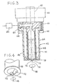
- FIGS. 2 through 4 show the writing head unit 20, and two writing heads 42, 44 are rotatably mounted with respect to a support plate 46.
- the support plate 46 is designed to be lifted and lowered by a drive servo motor 48 through a gear mechanism (not shown).
- the servo motor 48 includes a pulse encoder, of which pulse output is counted to control the rotation. Since the writing heads 42, 44 are almost identical in structure, the writing head 42 is explained below as representative along with FIGS. 3 and 4.
- On the support plate 46 is rotatably mounted a rotating member 60 around a shaft of rotation 62. Awarm watertank 64 is fixed to this rotating member 60 by nuts 66.
- This hot water tank is cylindrical, and a paste tank 68 is placed in the central hole of this cylinder so as to be put in and taken out freely.
- the paste tank 68 is filled with paste 70 for forming resistors and other elements of a thick film circuit.
- the paste 70 in an ordinary state, does not leak out from a long-length hole (for example, a slit of 100 p in length and 1 mm in width) 74 in a nozzle portion 72 disposed at the end of the tank 68.
- a diamond stylus tip 76 of about 40 p in height is disposed near the hole 74 at the end surface of the nozzle portion 72.
- the paste tank 68 is prevented from slipping out by screwing a ring-shaped cover 78 to the end of the warm water tank 64.
- the rotating mem ber 60 is also furnished with an air passage 80 for sending the air under pressure.
- the paste 68 is forced out from the hole 74 in the nozzle portion 72.
- the paste is changed or replenished by removing the cover 78 and taking out the paste tank 68.
- the warm water tank 64 is designed to receive warm water, especially a constant temperature water (at, for example, 25°C ⁇ 0.2°C), from an inlet 84 and discharge from an outlet 86.
- the paste 70 may be maintained at a constant temperature and constant viscosity, so that the delivery of paste per unit time from the nozzle portion 72 may be controlled at a constant quantity.
- the writing head 42 is, as mentioned above, rotatable, and its rotation center axis 88 runs through the center of the hole 74 in the nozzle portion 72. Therefore, however fast the writing head 42 may rotate, the center position of the hole 74 does not change and is definitely defined. Meanwhile, the mechanisms of the X-axis, Y-axis, Z-axis drive units 32, 34, 28, 30, 24, 46 and electromagnetic air valve 82 are controlled by a microcomputer (not shown). That is, the sequence of operation of the apparatus mentioned below is stored in the microcomputer, and the apparatus is designed to operate according to this stored sequence.
- writing operation is executed basically as follows.
- the writing head 42 descends, and its stylus tip 76 abuts against a conductor 92 on a thick film circuit board 90. At this time, a pressure of 50 to 100 grams is applied in the arrow direction in FIG. 5.
- the writing head moves in the arrow direction in FIG. 7 while its stylus tip 76 is contacting with the conductor 92 and the surface of the board 90.
- the writing head 42 comes to a specified position on other conductor 94 as shown in FIG. 7, it ascends, and a resistor 96 is formed.
- the extrusion operation of the paste 70 is conducted as follows. That is, in the apparatus of this embodiment, the paste 70 comes to be forced out simultaneously when the writing head 42 begins to move horizontally along the top surface of the board 90, and it ceases when the head stops.
- the writing head 42 is controlled by the microcomputer to move horizontally from an arbitrary point, and when it reaches above the conductor 92 on the board 90, it begins to lower toward the alumina ceramic board 90 which is used as the base of a thick film circuit.
- the travel from the highest position of the head 42 to the position abutting against the board 90 can be detected by the number of encoder pulses of the drive servo motor 48. By counting the number of pulses, it is detected when the head 42 comes to a certain position before abutting against the board 90, and the electromagnetic air valve 82 is opened at the same time.
- an air pressure begins to be applied to the paste 70.
- the time t 2 from application of release signal to the air valve till the actual application of air pressure to the paste is about 4 ms, but since this duration varies in each apparatus, in particular, the time required to release the electromagnetic air valve, t, is made variable so that the timing may be adjusted.
- the variable width of t is 1 to 9 ms.
- the writing head 42 is moved toward the conductor 94 at a high speed of 30 to 50 mm per second until reaching the position shown in FIG. 6, i.e., the position X in FIG. 8, when the application of control signal to the electromagnetic air valve 82 is stopped, and the pressure in the paste tank is released until equal to the atmospheric pressure.
- the extrusion of the paste 70 does not stop instantly due to the time required to close the electromagnetic air valve and the time for releasing the air in the paste tank 68 to the atmosphere, but it stops by the time when the writing nozzle portion 72 reaches a specified position on the conductor 94.
- This stop timing of the control signal applied to the electromagnetic air valve 82 is determined by counting the number of pulses from the X-axis, Y-axis drive pulse motors 52, 50. That is, the distance required for the nozzle portion 72 to move between conductors 92 and 94 is preliminarily counted by the number of pulses from the motor and preset in the microcomputer, and the pulses are counted down along with the movement of the nozzle portion, and when reaching a specified number of remaining counts, the control signal to the valve 82 is stopped. Of course, since this stopping position varies with each apparatus, the number of specified remaining pulses is variable and is made adjustable.
- the writing nozzle portion 72 goes up and moves to another arbitrary position, thus starts next writing similarly.
- a thick film resistor is written at a positional precision of 0.1 mm or less, and there is no defective pattern due to blurring or blotting either at the starting point or ending point of writing.
- the moving speed S of the writing nozzle portion and the acceleration 8 in starting and or ending are variable.
- the resistance of the resistor may be changed.
- the speed is reduced, the resistance is lowered, and when it is increased, the resistance is raised. This is possible because the output of paste per unit time is nearly constant.
- the acceleration in starting and/or ending the shape of writing at the start point and end point may be finely adjusted.
- the release control signal is sent to the electromagnetic air valve while the writing head is descending toward the board 90, but the same effect may be obtained by adopting the following sequence. That is, the release control signal is sent when the writing head descends completely on the board 90 (see M in FIG. 8) and the horizontal movement of the head is started when the paste is ready to be extruded a specified time after the completion of the head descending.
- the writing nozzle moves longitudinally, laterally and vertically while the board is fixed, but the same effect will be obtained when the writing nozzle is fixed and the board is moved longitudinally, laterally and vertically, or when the writing nozzle moves vertically while the board is moving longitudinally and laterally.
Landscapes
- Engineering & Computer Science (AREA)
- Manufacturing & Machinery (AREA)
- Microelectronics & Electronic Packaging (AREA)
- Manufacturing Of Printed Wiring (AREA)
- Coating Apparatus (AREA)
Applications Claiming Priority (2)
| Application Number | Priority Date | Filing Date | Title |
|---|---|---|---|
| JP152021/83 | 1983-08-19 | ||
| JP58152021A JPS6043894A (ja) | 1983-08-19 | 1983-08-19 | 厚膜回路の形成方法 |
Publications (3)
| Publication Number | Publication Date |
|---|---|
| EP0136020A2 EP0136020A2 (en) | 1985-04-03 |
| EP0136020A3 EP0136020A3 (en) | 1985-06-19 |
| EP0136020B1 true EP0136020B1 (en) | 1987-12-16 |
Family
ID=15531323
Family Applications (1)
| Application Number | Title | Priority Date | Filing Date |
|---|---|---|---|
| EP84305439A Expired EP0136020B1 (en) | 1983-08-19 | 1984-08-09 | Method and apparatus of forming patterns in thick film circuit or the like |
Country Status (5)
| Country | Link |
|---|---|
| US (1) | US4664945A (https=) |
| EP (1) | EP0136020B1 (https=) |
| JP (1) | JPS6043894A (https=) |
| CA (1) | CA1231464A (https=) |
| DE (1) | DE3468153D1 (https=) |
Families Citing this family (20)
| Publication number | Priority date | Publication date | Assignee | Title |
|---|---|---|---|---|
| US5108926A (en) * | 1987-09-08 | 1992-04-28 | Board Of Regents, The University Of Texas System | Apparatus for the precise positioning of cells |
| JPH01319990A (ja) * | 1988-06-22 | 1989-12-26 | Sumitomo Electric Ind Ltd | 厚膜形成方法 |
| US5232736A (en) * | 1989-07-24 | 1993-08-03 | Motorola, Inc. | Method for controlling solder printer |
| JPH0494592A (ja) * | 1990-08-10 | 1992-03-26 | Cmk Corp | プリント配線板におけるスルーホールに対する充填材の充填方法 |
| JPH0496400A (ja) * | 1990-08-13 | 1992-03-27 | Cmk Corp | シールド層を備えるプリント配線板の製造方法 |
| US5298288A (en) * | 1991-02-14 | 1994-03-29 | Microelectronics And Computer Technology Corporation | Coating a heat curable liquid dielectric on a substrate |
| US5151377A (en) * | 1991-03-07 | 1992-09-29 | Mobil Solar Energy Corporation | Method for forming contacts |
| US5641644A (en) * | 1994-12-09 | 1997-06-24 | Board Of Regents, The University Of Texas System | Method and apparatus for the precise positioning of cells |
| DE10004976C1 (de) | 2000-02-04 | 2001-09-13 | Foerdergemeinschaft Baeume Fue | Verfahren zum großflächigen Aufforsten |
| US6701835B2 (en) | 2001-07-31 | 2004-03-09 | Pilkington North America, Inc. | Method for placing indicia on substrates |
| JP4039035B2 (ja) * | 2001-10-31 | 2008-01-30 | セイコーエプソン株式会社 | 線パターンの形成方法、線パターン、電気光学装置、電子機器、非接触型カード媒体 |
| US20040238202A1 (en) * | 2003-06-02 | 2004-12-02 | Ohmcraft Inc. | Method of making an inductor with written wire and an inductor made therefrom |
| US20070169806A1 (en) * | 2006-01-20 | 2007-07-26 | Palo Alto Research Center Incorporated | Solar cell production using non-contact patterning and direct-write metallization |
| US7999175B2 (en) * | 2008-09-09 | 2011-08-16 | Palo Alto Research Center Incorporated | Interdigitated back contact silicon solar cells with laser ablated grooves |
| US9150966B2 (en) * | 2008-11-14 | 2015-10-06 | Palo Alto Research Center Incorporated | Solar cell metallization using inline electroless plating |
| US20120038031A1 (en) * | 2009-01-06 | 2012-02-16 | 1366 Technologies Inc. | Dispensing liquid containing material to patterned surfaces using a dispensing tube |
| US8962424B2 (en) | 2011-03-03 | 2015-02-24 | Palo Alto Research Center Incorporated | N-type silicon solar cell with contact/protection structures |
| US20130089656A1 (en) * | 2011-10-07 | 2013-04-11 | Sage Electrochromics, Inc. | Direct dispense device and method |
| EP3478034A4 (en) * | 2016-06-28 | 2019-07-03 | Fuji Corporation | SWITCHING PROCESS |
| DE112020003653T5 (de) * | 2019-07-29 | 2022-04-21 | Xtpl S.A. | Verfahren zum Abgeben einer metallischen Nanopartikelzusammensetzung aus einer Düse auf ein Substrat |
Family Cites Families (13)
| Publication number | Priority date | Publication date | Assignee | Title |
|---|---|---|---|---|
| US3645232A (en) * | 1970-03-10 | 1972-02-29 | Globe Union Inc | Apparatus for simultaneously applying a plurality of coatings to a substrate |
| US3961599A (en) * | 1971-08-12 | 1976-06-08 | Air Products And Chemicals, Inc. | Apparatus for making miniature layer resistors on insulating chips by digital controls |
| US3800020A (en) * | 1972-03-23 | 1974-03-26 | Cramer P Co | Method of making a circuit board |
| US3864695A (en) * | 1972-09-25 | 1975-02-04 | Asahi Optical Co Ltd | Pen having vertical movement control |
| US3820121A (en) * | 1972-10-13 | 1974-06-25 | Gerber Scientific Instr Co | Apparatus for expressing a writing fluid |
| DE2319997C2 (de) * | 1973-04-19 | 1975-06-12 | Licentia Patent-Verwaltungs-Gmbh, 6000 Frankfurt | Verfahren zur Herstellung mehrlagiger Leiterbahnenstrukturen auf einem Substrat mittels eines programmgesteuerten, für die Leiterbahnenherstellung herangezogenen Werkzeuges |
| DE2319998C2 (de) * | 1973-04-19 | 1975-06-12 | Licentia Patent-Verwaltungs-Gmbh, 6000 Frankfurt | Verfahren zur Herstellung mehrlagiger Leiterbahnenstrukturen auf einem Substrat mittels eines programmgesteuerten, für die Leiterbahnenherstellung herangezogenen Werkzeuges |
| US4133910A (en) * | 1977-12-01 | 1979-01-09 | The United States Of America As Represented By The Secretary Of The Army | Thick film deposition of microelectronic circuit |
| US4324815A (en) * | 1978-01-24 | 1982-04-13 | Mitani Electronics Industry Corp. | Screen-printing mask and method |
| US4327124A (en) * | 1978-07-28 | 1982-04-27 | Desmarais Jr Raymond C | Method for manufacturing printed circuits comprising printing conductive ink on dielectric surface |
| US4291642A (en) * | 1979-12-26 | 1981-09-29 | Rca Corporation | Nozzle for dispensing viscous fluid |
| US4338351A (en) * | 1980-09-10 | 1982-07-06 | Cts Corporation | Apparatus and method for producing uniform fired resistors |
| US4485387A (en) * | 1982-10-26 | 1984-11-27 | Microscience Systems Corp. | Inking system for producing circuit patterns |
-
1983
- 1983-08-19 JP JP58152021A patent/JPS6043894A/ja active Granted
-
1984
- 1984-08-08 US US06/638,713 patent/US4664945A/en not_active Expired - Lifetime
- 1984-08-09 EP EP84305439A patent/EP0136020B1/en not_active Expired
- 1984-08-09 DE DE8484305439T patent/DE3468153D1/de not_active Expired
- 1984-08-15 CA CA000461027A patent/CA1231464A/en not_active Expired
Also Published As
| Publication number | Publication date |
|---|---|
| JPS6043894A (ja) | 1985-03-08 |
| DE3468153D1 (en) | 1988-01-28 |
| US4664945A (en) | 1987-05-12 |
| JPH0370394B2 (https=) | 1991-11-07 |
| CA1231464A (en) | 1988-01-12 |
| EP0136020A2 (en) | 1985-04-03 |
| EP0136020A3 (en) | 1985-06-19 |
Similar Documents
| Publication | Publication Date | Title |
|---|---|---|
| EP0136020B1 (en) | Method and apparatus of forming patterns in thick film circuit or the like | |
| US4767489A (en) | Computer aided printer-etcher | |
| US4743465A (en) | Method and apparatus for drawing thick film circuit | |
| US4946708A (en) | Pin transfer adhesive application for surface mount component processes | |
| JP2000244107A (ja) | 吐出量制御機能付きディスペンサ及びクリーム半田の塗布方法 | |
| US5611480A (en) | Soldering process | |
| JPH05329421A (ja) | ボンド塗布装置 | |
| JPH0738500B2 (ja) | 塗布装置 | |
| JP2811947B2 (ja) | 電子部品の実装方法 | |
| JPS63270574A (ja) | 接着剤塗布装置 | |
| JPH05208263A (ja) | プリント基板の半田ディップ装置 | |
| JPS63160400A (ja) | 電子部品装着装置 | |
| JPH0537495Y2 (https=) | ||
| JPH0785513B2 (ja) | 接着剤塗布方法 | |
| JPH09271701A (ja) | 粘性体塗布装置 | |
| JP3513248B2 (ja) | 電子部品自動装着装置 | |
| JP3127577B2 (ja) | 電子部品のピックアップ装置及びピックアップ方法 | |
| JPS63173399A (ja) | 電子部品装着装置 | |
| JPS6213839B2 (https=) | ||
| JP2578935B2 (ja) | ダイボンディング装置 | |
| JPS59208895A (ja) | 厚膜回路形成方法 | |
| JPS63177590A (ja) | 電子部品の自動装着方法 | |
| JPH05220943A (ja) | 試行機能付き印字装置 | |
| JPH03161076A (ja) | 接着剤塗布装置 | |
| JPH0767034B2 (ja) | 部品装着装置 |
Legal Events
| Date | Code | Title | Description |
|---|---|---|---|
| PUAI | Public reference made under article 153(3) epc to a published international application that has entered the european phase |
Free format text: ORIGINAL CODE: 0009012 |
|
| AK | Designated contracting states |
Designated state(s): DE GB |
|
| PUAL | Search report despatched |
Free format text: ORIGINAL CODE: 0009013 |
|
| AK | Designated contracting states |
Designated state(s): DE GB |
|
| 17P | Request for examination filed |
Effective date: 19850909 |
|
| 17Q | First examination report despatched |
Effective date: 19860730 |
|
| GRAA | (expected) grant |
Free format text: ORIGINAL CODE: 0009210 |
|
| AK | Designated contracting states |
Kind code of ref document: B1 Designated state(s): DE GB |
|
| REF | Corresponds to: |
Ref document number: 3468153 Country of ref document: DE Date of ref document: 19880128 |
|
| PLBE | No opposition filed within time limit |
Free format text: ORIGINAL CODE: 0009261 |
|
| STAA | Information on the status of an ep patent application or granted ep patent |
Free format text: STATUS: NO OPPOSITION FILED WITHIN TIME LIMIT |
|
| 26N | No opposition filed | ||
| REG | Reference to a national code |
Ref country code: GB Ref legal event code: 746 Effective date: 19970901 |
|
| PGFP | Annual fee paid to national office [announced via postgrant information from national office to epo] |
Ref country code: GB Payment date: 19990804 Year of fee payment: 16 |
|
| PGFP | Annual fee paid to national office [announced via postgrant information from national office to epo] |
Ref country code: DE Payment date: 19990809 Year of fee payment: 16 |
|
| PG25 | Lapsed in a contracting state [announced via postgrant information from national office to epo] |
Ref country code: GB Free format text: LAPSE BECAUSE OF NON-PAYMENT OF DUE FEES Effective date: 20000809 |
|
| GBPC | Gb: european patent ceased through non-payment of renewal fee |
Effective date: 20000809 |
|
| PG25 | Lapsed in a contracting state [announced via postgrant information from national office to epo] |
Ref country code: DE Free format text: LAPSE BECAUSE OF NON-PAYMENT OF DUE FEES Effective date: 20010501 |