EP0116317B1 - Method for producing a semiconductor device comprising an oxidation step - Google Patents
Method for producing a semiconductor device comprising an oxidation step Download PDFInfo
- Publication number
- EP0116317B1 EP0116317B1 EP84100507A EP84100507A EP0116317B1 EP 0116317 B1 EP0116317 B1 EP 0116317B1 EP 84100507 A EP84100507 A EP 84100507A EP 84100507 A EP84100507 A EP 84100507A EP 0116317 B1 EP0116317 B1 EP 0116317B1
- Authority
- EP
- European Patent Office
- Prior art keywords
- film
- tungsten
- molybdenum
- silicon substrate
- sio2
- Prior art date
- Legal status (The legal status is an assumption and is not a legal conclusion. Google has not performed a legal analysis and makes no representation as to the accuracy of the status listed.)
- Expired - Lifetime
Links
Images


Classifications
-
- H—ELECTRICITY
- H10—SEMICONDUCTOR DEVICES; ELECTRIC SOLID-STATE DEVICES NOT OTHERWISE PROVIDED FOR
- H10D—INORGANIC ELECTRIC SEMICONDUCTOR DEVICES
- H10D64/00—Electrodes of devices having potential barriers
- H10D64/01—Manufacture or treatment
- H10D64/011—Manufacture or treatment of electrodes ohmically coupled to a semiconductor
-
- H—ELECTRICITY
- H10—SEMICONDUCTOR DEVICES; ELECTRIC SOLID-STATE DEVICES NOT OTHERWISE PROVIDED FOR
- H10P—GENERIC PROCESSES OR APPARATUS FOR THE MANUFACTURE OR TREATMENT OF DEVICES COVERED BY CLASS H10
- H10P14/00—Formation of materials, e.g. in the shape of layers or pillars
- H10P14/60—Formation of materials, e.g. in the shape of layers or pillars of insulating materials
- H10P14/63—Formation of materials, e.g. in the shape of layers or pillars of insulating materials characterised by the formation processes
- H10P14/6302—Non-deposition formation processes
- H10P14/6304—Formation by oxidation, e.g. oxidation of the substrate
- H10P14/6306—Formation by oxidation, e.g. oxidation of the substrate of the semiconductor materials
- H10P14/6308—Formation by oxidation, e.g. oxidation of the substrate of the semiconductor materials of Group IV semiconductors
- H10P14/6309—Formation by oxidation, e.g. oxidation of the substrate of the semiconductor materials of Group IV semiconductors of silicon in uncombined form, i.e. pure silicon
-
- H—ELECTRICITY
- H10—SEMICONDUCTOR DEVICES; ELECTRIC SOLID-STATE DEVICES NOT OTHERWISE PROVIDED FOR
- H10P—GENERIC PROCESSES OR APPARATUS FOR THE MANUFACTURE OR TREATMENT OF DEVICES COVERED BY CLASS H10
- H10P14/00—Formation of materials, e.g. in the shape of layers or pillars
- H10P14/60—Formation of materials, e.g. in the shape of layers or pillars of insulating materials
- H10P14/61—Formation of materials, e.g. in the shape of layers or pillars of insulating materials using masks
-
- H—ELECTRICITY
- H10—SEMICONDUCTOR DEVICES; ELECTRIC SOLID-STATE DEVICES NOT OTHERWISE PROVIDED FOR
- H10P—GENERIC PROCESSES OR APPARATUS FOR THE MANUFACTURE OR TREATMENT OF DEVICES COVERED BY CLASS H10
- H10P14/00—Formation of materials, e.g. in the shape of layers or pillars
- H10P14/60—Formation of materials, e.g. in the shape of layers or pillars of insulating materials
- H10P14/63—Formation of materials, e.g. in the shape of layers or pillars of insulating materials characterised by the formation processes
- H10P14/6302—Non-deposition formation processes
- H10P14/6322—Formation by thermal treatments
-
- H—ELECTRICITY
- H10—SEMICONDUCTOR DEVICES; ELECTRIC SOLID-STATE DEVICES NOT OTHERWISE PROVIDED FOR
- H10P—GENERIC PROCESSES OR APPARATUS FOR THE MANUFACTURE OR TREATMENT OF DEVICES COVERED BY CLASS H10
- H10P14/00—Formation of materials, e.g. in the shape of layers or pillars
- H10P14/60—Formation of materials, e.g. in the shape of layers or pillars of insulating materials
- H10P14/69—Inorganic materials
- H10P14/692—Inorganic materials composed of oxides, glassy oxides or oxide-based glasses
- H10P14/6921—Inorganic materials composed of oxides, glassy oxides or oxide-based glasses containing silicon
- H10P14/69215—Inorganic materials composed of oxides, glassy oxides or oxide-based glasses containing silicon the material being a silicon oxide, e.g. SiO2
-
- H—ELECTRICITY
- H10—SEMICONDUCTOR DEVICES; ELECTRIC SOLID-STATE DEVICES NOT OTHERWISE PROVIDED FOR
- H10P—GENERIC PROCESSES OR APPARATUS FOR THE MANUFACTURE OR TREATMENT OF DEVICES COVERED BY CLASS H10
- H10P30/00—Ion implantation into wafers, substrates or parts of devices
- H10P30/20—Ion implantation into wafers, substrates or parts of devices into semiconductor materials, e.g. for doping
- H10P30/22—Ion implantation into wafers, substrates or parts of devices into semiconductor materials, e.g. for doping using masks
-
- H—ELECTRICITY
- H10—SEMICONDUCTOR DEVICES; ELECTRIC SOLID-STATE DEVICES NOT OTHERWISE PROVIDED FOR
- H10P—GENERIC PROCESSES OR APPARATUS FOR THE MANUFACTURE OR TREATMENT OF DEVICES COVERED BY CLASS H10
- H10P76/00—Manufacture or treatment of masks on semiconductor bodies, e.g. by lithography or photolithography
- H10P76/40—Manufacture or treatment of masks on semiconductor bodies, e.g. by lithography or photolithography of masks comprising inorganic materials
- H10P76/405—Manufacture or treatment of masks on semiconductor bodies, e.g. by lithography or photolithography of masks comprising inorganic materials characterised by their composition, e.g. multilayer masks
-
- H—ELECTRICITY
- H10—SEMICONDUCTOR DEVICES; ELECTRIC SOLID-STATE DEVICES NOT OTHERWISE PROVIDED FOR
- H10P—GENERIC PROCESSES OR APPARATUS FOR THE MANUFACTURE OR TREATMENT OF DEVICES COVERED BY CLASS H10
- H10P95/00—Generic processes or apparatus for manufacture or treatments not covered by the other groups of this subclass
-
- H—ELECTRICITY
- H10—SEMICONDUCTOR DEVICES; ELECTRIC SOLID-STATE DEVICES NOT OTHERWISE PROVIDED FOR
- H10W—GENERIC PACKAGES, INTERCONNECTIONS, CONNECTORS OR OTHER CONSTRUCTIONAL DETAILS OF DEVICES COVERED BY CLASS H10
- H10W10/00—Isolation regions in semiconductor bodies between components of integrated devices
- H10W10/01—Manufacture or treatment
- H10W10/011—Manufacture or treatment of isolation regions comprising dielectric materials
- H10W10/012—Manufacture or treatment of isolation regions comprising dielectric materials using local oxidation of silicon [LOCOS]
- H10W10/0125—Manufacture or treatment of isolation regions comprising dielectric materials using local oxidation of silicon [LOCOS] comprising introducing electrical impurities in local oxidation regions, e.g. to alter LOCOS oxide growth characteristics
- H10W10/0126—Manufacture or treatment of isolation regions comprising dielectric materials using local oxidation of silicon [LOCOS] comprising introducing electrical impurities in local oxidation regions, e.g. to alter LOCOS oxide growth characteristics introducing electrical active impurities in local oxidation regions to create channel stoppers
-
- H—ELECTRICITY
- H10—SEMICONDUCTOR DEVICES; ELECTRIC SOLID-STATE DEVICES NOT OTHERWISE PROVIDED FOR
- H10W—GENERIC PACKAGES, INTERCONNECTIONS, CONNECTORS OR OTHER CONSTRUCTIONAL DETAILS OF DEVICES COVERED BY CLASS H10
- H10W10/00—Isolation regions in semiconductor bodies between components of integrated devices
- H10W10/10—Isolation regions comprising dielectric materials
- H10W10/13—Isolation regions comprising dielectric materials formed using local oxidation of silicon [LOCOS], e.g. sealed interface localised oxidation [SILO] or side-wall mask isolation [SWAMI]
-
- Y—GENERAL TAGGING OF NEW TECHNOLOGICAL DEVELOPMENTS; GENERAL TAGGING OF CROSS-SECTIONAL TECHNOLOGIES SPANNING OVER SEVERAL SECTIONS OF THE IPC; TECHNICAL SUBJECTS COVERED BY FORMER USPC CROSS-REFERENCE ART COLLECTIONS [XRACs] AND DIGESTS
- Y10—TECHNICAL SUBJECTS COVERED BY FORMER USPC
- Y10S—TECHNICAL SUBJECTS COVERED BY FORMER USPC CROSS-REFERENCE ART COLLECTIONS [XRACs] AND DIGESTS
- Y10S438/00—Semiconductor device manufacturing: process
- Y10S438/909—Controlled atmosphere
Definitions
- This invention relates to a method of producing a semiconductor device equipped with electrodes and interconnections consisting of tungsten or molybdenum.
- polycrystalline silicon has been used widely as a material for electrodes and interconnections of a semiconductor device.
- Polycrystalline silicon has been used for the following reasons. In order to miniaturize an MIS transistor, it is inevitable to employ so-called "self-alignment” techniques which form source and drain by ion implantation using the gate electrode as the mask. After ion-implantation is completed, however, annealing at high temperatures must be made by all means to remove damage of the source and drain region that has developed due to ion-implantation.
- the gate electrode must be made of a material which can withstand the heat-treatment at high temperatures, and polycrystalline silicon having a high melting point has replaced aluminum that was used widely and previously.
- tungsten or molybdenum have been proposed in place of polycrystalline silicon so as to form electrodes and interconnections. Since tungsten or molybdenum have a high melting point, they can withstand annealing at high temperatures and moreover, since their electric resistance is far lower than that of polycrystalline silicon, the problem described above, that occurs when polycrystalline silicon is used, does not develop even when the width of the electrode or interconnection is extremely small.
- tungsten and molybdenum have the problem that they are more easily oxidized than silicon.
- heat-treatment is carried out at about 300°C or above in an oxidizing atmosphere, therefore, they are rapidly oxidized, disclosed or peeled off from the substrate.
- An insulating film (SiO2 film) deposited on a semiconductor substrate is damaged or contaminated if an ion-implantation is effected using the gate as the mask to form the source and drain during the fabrication of an MOS transistor. Accordingly, the damaged or contaminated insulating film must be removed by etching after completion of gate formation and ion-implantation and the heat-treatment is carried out in an oxidizing atmosphere to re-grow an SiO2 film on the semiconductor substrate. This process is carried out generally and widely and is an indispensable step to form a high reliability MOS transistor. (This process or treatment will be hereinafter referred to as "light oxidation").
- the gate electrode and the interconnections When polycristalline silicon is used for the gate electrode and the interconnections, the light oxidation described above can be carried out smoothly without any problems.
- the gate electrode and interconnections are highly oxidized because tungsten and molybdenum are extremely oxidizable. Therefore, such semiconductors having high reliability and a high integration density cannot be produced.
- the present invention is directed to provide a method of producing a semiconductor device in which electrodes and interconnections are formed by using tungsten or molybdenum without any problems.
- the present invention is directed to provide a method of producing a semiconductor device in which silicon is oxidized selectively without substantially oxidizing tungsten or molybdenum.
- Si and most metals form their oxides upon reacting with water vapor.
- the SiO2 film can be formed on the Si substrate without oxidizing the electrodes and interconnections made of W or Mo, and the present invention is extremely advantageous for the fabrication of the MOS transistors having high integration density.
- the heat-treating temperature is selected in the range of from about 400 to about 1,200°C.
- the W and Mo films were not mostly oxidized but there were also the cases in which only the film edge portions were oxidized or the entire surface of the film was oxidized, so that a stable result could not be obtained.
- the Si surface was oxidized in all cases.
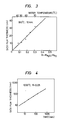
- This example illustrates the relation between the oxidation of Si and the partial pressure ratio R of H2O and H2 the atmosphere when heating is effected in the H2/H2O atmosphere.
- the vapor-containing hydrogen could be obtained by passing hydrogen through a bubbler containing pure water, and the vapor quantity in hydrogen could be adjusted to a desired value by changing the temperature of the pure water in the bubbler.
- heat-treatment was carried out at 950°C for 10 minutes by changing the ratio R and the thickness of the SiO2 film formed on the silicon wafer was measured using an ellipsometer.
- the silicon wafer used for the measurement was washed by hydrofluoric acid before heating to remove in advance the oxide film on the wafer surface.
- the result obtained was shown in Figure 3.
- the thickness of the SiO2 film increased substantially proportionally to the value R within the range of O ⁇ R ⁇ 0.4.
- Figure 4 shows the result of the measurement of time dependence of the thickness of the SiO2 film when the heating temperature was 1,000°C and R was 0.05.
- Figure 5 shows the dependence of the thickness of the SiO2 film upon the heating temperature when R was 0.05.
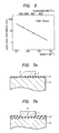
- This example illustrates the application of the present invention to the fabrication of an MOS field effect transistor.
- a tungsten film 1 and a silicon dioxide film 2' were formed sequentially in thickness of 350 nm and 60 nm, respectively, on a 20 nm-thick silicon dioxide film 2 that was formed on the surface of a silicon substrate 3.
- the silicon dioxide film 2' and the tungsten film 1 were then patterned sequentially into the pattern of a gate electrode by known dry etching techniques.
- an impurity ion was implanted into the silicon substrate 3 through the silicon dioxide film 2 using the electrode consisting of the silicon dioxide film 2' and the tungsten film 1 as the mask, to form a source and drain 4 as shown in Figure 6b.
- the silicon oxide films 2, 2' at the portions other than the portion covered with the W film 1 were selectively removed using a hydrofluoric acid solution diluted to 1/10 by water, as shown in Figure 6c.
- the heat-treatment was effected at 900°C for 15 minutes in hydrogen containing 5% of vapor to grow an about 10 nm-thick silicon dioxide film 2'' on the exposed silicon substrate 3 as shown in Figure 6d.
- a phosphoglass layer 5 was deposited in a thickness of about 500 nm over the entire surface and contact holes were bored by photoetching.
- Aluminum interconnections 6 were formed to complete the MOS transistor as shown in Figure 6e.
- This example corresponds to the light oxidation step in the silicon gate process, and the tungsten gate transistor produced by this step exhibited the improvement in the MOS characteristics (break-down voltage of the SiO2 film and variance of breakdown voltage).
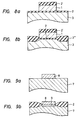
- a 350 nm-thick tungsten film 1 was deposited and patterned on a 20 nm-thick SiO2 film 2 that was formed on a Si single crystal substrate 3 as shown in Figure 7a.
- Heat-treatment was effected at 1,000°C for one hour in hydrogen passed through a bubbler of pure water (hydrogen containing about 3% of water), whereby the thickness d1 of the SiO2 film 2 of the portion covered with the tungsten film 1 and the thickness d2 at the portion not covered with the tungsten film 1 increased to 30 nm and 70 nm, respectively.
- the tungsten fim 1 was not oxidized.
- the moisture content in hydrogen, heating temperature and heating time were increased (or decreased) in accordance with Example 2 and the thickness d1 and d2 of the SiO2 film increased (or decreased) in response to the former.
- the breakdown voltage of the SiO2 film was measured using the tungsten film as the electrode. The breakdown voltage was found increased than before the heat-treatment. It was thus confirmed that the present invention could effectively prevent degradation of the characteristics of the SiO2 film due to the heat-treatment.
- a 300 nm-thick tungsten film 1 was vacuum deposited on a 20 nm-thick SiO2 film 2 that was formed on an Si crystal substrate 3 as shown in Figure 8a, and an 80 nm-thick SiO2 film 2' was deposited by CVD on the tungsten film 1. Unnecessary portions were removed by sequentially etching the SiO2 film 2' and the tungsten film 1.
- the sample was then heated at 900 to 1,000°C for 15 minutes in hydrogen containing 3 to 20% of water, whereby the portion of the SiO2 film 2''' not covered with the tungsten film 1 became thicker in the same way as in Example 4 but the thickness of the SiO2 film 2 below the tungsten film 1 remained substantially unaltered, as shown in Figure 8b.
- those materials at least one of polycrystalline Si, PSG, SiO2, Si3N4 and the like
- the function of the mask for the prevention of oxidation can be more improved than when heat-treatment is carried out using the tungsten film alone.
- a 350 nm-thick molybdenum film 8 was vacuum deposited on a polycrystalline silicon substrate 7 as shown in Figure 9a and unnecessary portions were removed by etching the film 8.
- the sample was heat-treated at 900°C for 30 minutes in hydrogen containing 5% of vapor.
- the molybdenum film 8 reacted with the polycrystalline silicon substrate 7 and a molybdenum silicide layer 9 was formed at their contact portion.
- the portion of the surface of the polycrystalline silicon substrate 7 at which the molybdenum film 8 did not exist and which was exposed was oxidized to form a thick SiO2 film 2.
- contact could be established between the molybdenum film and the polycrystalline silicon substrate and at the same time, an insulating film could be formed on the polycrystalline silicon in self-alignment with the molybdenum electrode. Substantially the same result could be obtained by use of a tungsten film in place of the molybdenum film.
- FIGS 10a through 10c illustrate another method of producing an MOS field effect semiconductor device to which the present invention is applied.
- an about 350 nm-thick tungsten film was formed on a 20 nm-thick field insulating film (SiO2 film) 2 (reference numeral 2''' represents a field silicon diode film formed in advance) that was formed on the surface of an Si crystal substrate 3.
- the tungsten film was then patterned to form a gate electrode 1.
- the sample was heated in an oxygen atmosphere of about 400°C to form an about 50 nm-thick tungsten oxide film 10 on the surface of the tungsten film 1 as shown in Figure 10b.
- the tungsten oxide film 10 and the tungsten film 1 as the mask, an impurity was doped to the surface region of the Si substrate 3 and the sample was heat-treated at 950°C for 30 minutes in hydrogen containing 5% of vapor, thereby forming source and drain region 4.
- the tungsten oxide film 10 on the surface of the tungsten film 1 served as the mask for doping the impurity by ion implantation or the like, and was reduced to tungsten due to the subsequent heat-treatment in the H2O-H2 atmosphere, as shown in Figure 10c. Due to the heat-treatment described above, the silicon oxide film on the source-drain region 4 became thicker than the oxide film below the gate electrode.
- An about 250 nm-thick molybdenum silicide film 9 was formed on the surface of a 300 nm-thick polycrystalline silicon plate 7 as shown in Figure 11a and a molybdenum film 8 was vacuum deposited on it in a thickness of about 300 nm. Unnecessary portions were removed by etching to form an electrode 8. The sample was heated at 900°C for 10 minutes in hydrogen containing 5% of water, whereby a part of the molybdenum electrode 8 was converted to its silicide, and an SiO2 film 2 was formed on the exposed surface of the resulting molybdenum silicide film 9.
- the present invention makes it possible to grow the SiO2 film not only on Si but also on the silicide film.
- tungsten silicide When tungsten silicide was used in place of molybdenum silicide, the exposed surface of tungsten silicide could also be oxidized without oxidizing molybdenum and tungsten.
- a 350 nm-thick tungsten film 1 was deposited on a 20 nm-thick gate SiO2 film 2 that was formed on an Si crystal substrate 3.
- the SiO2 film around the gate electrode was also damaged so that the SiO2 film became thinner by about 10 nm and the breakdown voltage of the gate SiO2 film got deteriorated.
- the damage of the SiO2 film was recovered and at the same time, a fresh SiO2 film grew. Accordingly, the breakdown voltage of the gate SiO2 film was improved.
- This heat-treatment may be effected after etching and removing the SiO2 film around the gate, and the same result could be obtained when the heat-treatment was effected without removing the SiO2 film.
- the following two kinds of wafers were prepared. First, an Si wafer having formed a tungsten film on the surface thereof was heated in an oxygen atmosphere to form a 300 nm-thick tungsten oxide film. Separately, an Si wafer was washed by hydrofluoric acid to prepare a wafer (up to 2 nm thick) hardly having any oxide film. These two kinds of wafers were heated at 1,000°C for 1 hour in hydrogen containing 3% of water and their surfaces were analyzed by X-ray photoelectronic spectrometry. As a result, the tungsten oxide was reduced to tungsten due to the heat-treatment but the Si wafers were oxidized and an SiO2 film was formed on the surface. The resulting SiO2 film was found to be 58 nm thick as a result of measurement by an elipsometer.
- silicon can be selectively oxidized without oxidizing tungsten and molybdenum during the fabrication of a semiconductor device by using H2O/H2 as the atmosphere of heat-treatment and by adjusting their partial pressure ratio.
- the so-called "light oxidation" process that has been employed in the conventional polycrystalline silicon gate process, can be also used in the fabrication process of MOS transistors using tungsten or molybdenum for the gate.
- the present invention eliminates the problem of oxidation of tungsten and molybdenum during fabrication of semiconductor devices and a process approximate to the one used in the conventional polycrystalline silicon process can now be used.
- the characteristics of the resulting device can be remarkably stabilized in comparison with the tungsten or molybdenum gate process not using the H2O/H2 heat-treatment.
- the present invention made it possible to carry out "glass flow" without the possibility of oxidation of W or Mo.
- the present invention makes it possible to selectively oxidize only Si and to form an SiO2 film without oxidizing W or Mo and to remarkably improve the reliability and producibility of semiconductor devices using these materials.
- W or Mo is used as the low resistance electrode of an MOS field effect semiconductor device
- compatibility with the Si gate process can be improved.
- the "light oxidation" process becomes feasible.
- the present invention uses hydrogen containing water as the heating atmosphere, it can be easily practised using an ordinary heating apparatus consisting of a silica tube and an electric furnace and is excellent in both mass-producibility and economy.
Landscapes
- Insulated Gate Type Field-Effect Transistor (AREA)
- Electrodes Of Semiconductors (AREA)
- Formation Of Insulating Films (AREA)
- Local Oxidation Of Silicon (AREA)
- Internal Circuitry In Semiconductor Integrated Circuit Devices (AREA)
Applications Claiming Priority (2)
| Application Number | Priority Date | Filing Date | Title |
|---|---|---|---|
| JP58006868A JPS59132136A (ja) | 1983-01-19 | 1983-01-19 | 半導体装置の製造方法 |
| JP6868/83 | 1983-01-19 |
Publications (3)
| Publication Number | Publication Date |
|---|---|
| EP0116317A2 EP0116317A2 (en) | 1984-08-22 |
| EP0116317A3 EP0116317A3 (en) | 1987-07-22 |
| EP0116317B1 true EP0116317B1 (en) | 1992-04-01 |
Family
ID=11650210
Family Applications (1)
| Application Number | Title | Priority Date | Filing Date |
|---|---|---|---|
| EP84100507A Expired - Lifetime EP0116317B1 (en) | 1983-01-19 | 1984-01-18 | Method for producing a semiconductor device comprising an oxidation step |
Country Status (5)
| Country | Link |
|---|---|
| US (1) | US4505028A (OSRAM) |
| EP (1) | EP0116317B1 (OSRAM) |
| JP (1) | JPS59132136A (OSRAM) |
| KR (1) | KR910007097B1 (OSRAM) |
| DE (1) | DE3485622D1 (OSRAM) |
Cited By (1)
| Publication number | Priority date | Publication date | Assignee | Title |
|---|---|---|---|---|
| DE10236896A1 (de) * | 2002-08-12 | 2004-04-01 | Infineon Technologies Ag | Vorrichtung und Verfahren zum thermischen Behandeln von Halbleiterwafern |
Families Citing this family (36)
| Publication number | Priority date | Publication date | Assignee | Title |
|---|---|---|---|---|
| US4587710A (en) * | 1984-06-15 | 1986-05-13 | Gould Inc. | Method of fabricating a Schottky barrier field effect transistor |
| US5907188A (en) * | 1995-08-25 | 1999-05-25 | Kabushiki Kaisha Toshiba | Semiconductor device with conductive oxidation preventing film and method for manufacturing the same |
| US5789312A (en) * | 1996-10-30 | 1998-08-04 | International Business Machines Corporation | Method of fabricating mid-gap metal gates compatible with ultra-thin dielectrics |
| JPH10223900A (ja) * | 1996-12-03 | 1998-08-21 | Toshiba Corp | 半導体装置及び半導体装置の製造方法 |
| US6893980B1 (en) * | 1996-12-03 | 2005-05-17 | Kabushiki Kaisha Toshiba | Semiconductor device and manufacturing method therefor |
| TW462093B (en) | 1997-03-05 | 2001-11-01 | Hitachi Ltd | Method for manufacturing semiconductor integrated circuit device having a thin insulative film |
| JPH10335652A (ja) | 1997-05-30 | 1998-12-18 | Hitachi Ltd | 半導体集積回路装置の製造方法 |
| JPH10340909A (ja) | 1997-06-06 | 1998-12-22 | Hitachi Ltd | 半導体集積回路装置の製造方法 |
| JP4283904B2 (ja) | 1997-07-11 | 2009-06-24 | 株式会社東芝 | 半導体装置の製造方法 |
| US6159866A (en) * | 1998-03-02 | 2000-12-12 | Applied Materials, Inc. | Method for insitu vapor generation for forming an oxide on a substrate |
| US6037273A (en) * | 1997-07-11 | 2000-03-14 | Applied Materials, Inc. | Method and apparatus for insitu vapor generation |
| EP0910119B1 (en) * | 1997-10-14 | 2009-06-03 | Texas Instruments Incorporated | Method for oxidizing a structure during the fabrication of a semiconductor device |
| US6452276B1 (en) | 1998-04-30 | 2002-09-17 | International Business Machines Corporation | Ultra thin, single phase, diffusion barrier for metal conductors |
| JPH11330468A (ja) | 1998-05-20 | 1999-11-30 | Hitachi Ltd | 半導体集積回路装置の製造方法および半導体集積回路装置 |
| US6835672B1 (en) * | 1998-10-15 | 2004-12-28 | Texas Instruments Incorporated | Selective oxidation for semiconductor device fabrication |
| US6162694A (en) * | 1998-11-25 | 2000-12-19 | Advanced Micro Devices, Inc. | Method of forming a metal gate electrode using replaced polysilicon structure |
| DE19901210A1 (de) * | 1999-01-14 | 2000-07-27 | Siemens Ag | Halbleiterbauelement und Verfahren zu dessen Herstellung |
| JP2000349285A (ja) * | 1999-06-04 | 2000-12-15 | Hitachi Ltd | 半導体集積回路装置の製造方法および半導体集積回路装置 |
| TW434704B (en) * | 1999-06-11 | 2001-05-16 | Univ Nat Yunlin Sci & Tech | Device of amorphous WO3 ion sensitive field effect transistor (ISFET) and method for making the same |
| US6555407B1 (en) | 1999-10-26 | 2003-04-29 | Zarlink Semiconductor Ab | Method for the controlled oxidiation of materials |
| GB2355850A (en) * | 1999-10-26 | 2001-05-02 | Mitel Semiconductor Ab | Forming oxide layers in semiconductor layers |
| JP2001274154A (ja) | 2000-01-18 | 2001-10-05 | Applied Materials Inc | 成膜方法、成膜装置、半導体装置及びその製造方法 |
| US6603181B2 (en) * | 2001-01-16 | 2003-08-05 | International Business Machines Corporation | MOS device having a passivated semiconductor-dielectric interface |
| CN1290197C (zh) | 2001-03-12 | 2006-12-13 | 株式会社日立制作所 | 用于制造半导体集成电路器件的方法 |
| KR100650467B1 (ko) * | 2001-03-12 | 2006-11-28 | 가부시키가이샤 히타치세이사쿠쇼 | 반도체 집적 회로 장치 및 그 제조 방법 |
| KR100402389B1 (ko) * | 2001-03-23 | 2003-10-17 | 삼성전자주식회사 | 금속 게이트 형성 방법 |
| DE10120523A1 (de) | 2001-04-26 | 2002-10-31 | Infineon Technologies Ag | Verfahren zur Minimierung der Wolframoxidausdampfung bei der selektiven Seitenwandoxidation von Wolfram-Silizium-Gates |
| TW200416772A (en) * | 2002-06-06 | 2004-09-01 | Asml Us Inc | System and method for hydrogen-rich selective oxidation |
| KR100459725B1 (ko) * | 2002-09-19 | 2004-12-03 | 삼성전자주식회사 | 금속 게이트 패턴을 갖는 반도체소자의 제조방법 |
| JP2005101141A (ja) * | 2003-09-24 | 2005-04-14 | Renesas Technology Corp | 半導体集積回路装置およびその製造方法 |
| US7981785B2 (en) * | 2004-03-01 | 2011-07-19 | Tokyo Electron Limited | Method for manufacturing semiconductor device and plasma oxidation method |
| WO2006095752A1 (ja) * | 2005-03-08 | 2006-09-14 | Hitachi Kokusai Electric Inc. | 半導体装置の製造方法および基板処理装置 |
| JP2007165788A (ja) * | 2005-12-16 | 2007-06-28 | Tokyo Electron Ltd | 金属系膜の脱炭素処理方法、成膜方法および半導体装置の製造方法 |
| US7951728B2 (en) * | 2007-09-24 | 2011-05-31 | Applied Materials, Inc. | Method of improving oxide growth rate of selective oxidation processes |
| US9127340B2 (en) * | 2009-02-13 | 2015-09-08 | Asm International N.V. | Selective oxidation process |
| US8889565B2 (en) * | 2009-02-13 | 2014-11-18 | Asm International N.V. | Selective removal of oxygen from metal-containing materials |
Family Cites Families (5)
| Publication number | Priority date | Publication date | Assignee | Title |
|---|---|---|---|---|
| US3679492A (en) * | 1970-03-23 | 1972-07-25 | Ibm | Process for making mosfet's |
| NL164424C (nl) * | 1970-06-04 | 1980-12-15 | Philips Nv | Werkwijze voor het vervaardigen van een veldeffect- transistor met een geisoleerde stuurelektrode, waarbij een door een tegen oxydatie maskerende laag vrijgelaten deel van het oppervlak van een siliciumlichaam aan een oxydatiebehandeling wordt onderworpen ter verkrijging van een althans gedeeltelijk in het siliciumlichaam verzonken siliciumoxydelaag. |
| US3959025A (en) * | 1974-05-01 | 1976-05-25 | Rca Corporation | Method of making an insulated gate field effect transistor |
| US4093503A (en) * | 1977-03-07 | 1978-06-06 | International Business Machines Corporation | Method for fabricating ultra-narrow metallic lines |
| JPS5693314A (en) * | 1979-12-26 | 1981-07-28 | Fujitsu Ltd | Ion injector |
-
1983
- 1983-01-19 JP JP58006868A patent/JPS59132136A/ja active Granted
-
1984
- 1984-01-18 EP EP84100507A patent/EP0116317B1/en not_active Expired - Lifetime
- 1984-01-18 KR KR1019840000207A patent/KR910007097B1/ko not_active Expired
- 1984-01-18 DE DE8484100507T patent/DE3485622D1/de not_active Expired - Lifetime
- 1984-01-19 US US06/571,946 patent/US4505028A/en not_active Expired - Lifetime
Non-Patent Citations (1)
| Title |
|---|
| IEEE Transactions on Electron Devices, vol. ED-26, No. 4, April 1979, pages 369-371 * |
Cited By (2)
| Publication number | Priority date | Publication date | Assignee | Title |
|---|---|---|---|---|
| DE10236896A1 (de) * | 2002-08-12 | 2004-04-01 | Infineon Technologies Ag | Vorrichtung und Verfahren zum thermischen Behandeln von Halbleiterwafern |
| DE10236896B4 (de) * | 2002-08-12 | 2010-08-12 | Mattson Thermal Products Gmbh | Vorrichtung und Verfahren zum thermischen Behandeln von Halbleiterwafern |
Also Published As
| Publication number | Publication date |
|---|---|
| KR840007307A (ko) | 1984-12-06 |
| US4505028A (en) | 1985-03-19 |
| KR910007097B1 (ko) | 1991-09-18 |
| EP0116317A3 (en) | 1987-07-22 |
| EP0116317A2 (en) | 1984-08-22 |
| DE3485622D1 (de) | 1992-05-07 |
| JPH0458688B2 (OSRAM) | 1992-09-18 |
| JPS59132136A (ja) | 1984-07-30 |
Similar Documents
| Publication | Publication Date | Title |
|---|---|---|
| EP0116317B1 (en) | Method for producing a semiconductor device comprising an oxidation step | |
| US4701349A (en) | Semiconductor integrated circuit device and method of producing the same | |
| EP1361614B1 (en) | Semiconductor device manufacturing method | |
| US5324974A (en) | Nitride capped MOSFET for integrated circuits | |
| US6727148B1 (en) | ULSI MOS with high dielectric constant gate insulator | |
| KR960013135B1 (ko) | 캡 산화물을 배치한 티탄 규화물 형성 방법 | |
| US5089432A (en) | Polycide gate MOSFET process for integrated circuits | |
| EP0617461A2 (en) | Oxynitride dielectric process for IC manufacture | |
| JPS63316476A (ja) | 半導体装置およびその製造方法 | |
| JPH05211330A (ja) | 電界効果トランジスタおよびその製造方法 | |
| US5214305A (en) | Polycide gate MOSFET for integrated circuits | |
| US20050130380A1 (en) | Semiconductor device structures including metal silicide interconnects and dielectric layers at substantially the same fabrication level | |
| US5130266A (en) | Polycide gate MOSFET process for integrated circuits | |
| US4551907A (en) | Process for fabricating a semiconductor device | |
| US5652183A (en) | Method for fabricating semiconductor device containing excessive silicon in metal silicide film | |
| JPS6298642A (ja) | 半導体集積回路装置の製造方法 | |
| US5288666A (en) | Process for forming self-aligned titanium silicide by heating in an oxygen rich environment | |
| US6444532B2 (en) | Process for fabricating MOS semiconductor transistor | |
| JPH08116057A (ja) | 半導体装置のTiNゲート電極の製造方法 | |
| JPH1167760A (ja) | 半導体装置の製造方法 | |
| US7166525B2 (en) | High temperature hydrogen annealing of a gate insulator layer to increase etching selectivity between conductive gate structure and gate insulator layer | |
| JP3376158B2 (ja) | 半導体装置の製造方法 | |
| JP3185235B2 (ja) | 半導体装置の製造方法 | |
| US5108953A (en) | Method for fabricating a semiconductive device comprising a refractory metal silicide thin film | |
| JPS60124972A (ja) | 半導体装置の製造方法 |
Legal Events
| Date | Code | Title | Description |
|---|---|---|---|
| PUAI | Public reference made under article 153(3) epc to a published international application that has entered the european phase |
Free format text: ORIGINAL CODE: 0009012 |
|
| AK | Designated contracting states |
Designated state(s): DE FR GB IT |
|
| 17P | Request for examination filed |
Effective date: 19841220 |
|
| PUAL | Search report despatched |
Free format text: ORIGINAL CODE: 0009013 |
|
| AK | Designated contracting states |
Kind code of ref document: A3 Designated state(s): DE FR GB IT |
|
| 17Q | First examination report despatched |
Effective date: 19890905 |
|
| GRAA | (expected) grant |
Free format text: ORIGINAL CODE: 0009210 |
|
| AK | Designated contracting states |
Kind code of ref document: B1 Designated state(s): DE FR GB IT |
|
| PG25 | Lapsed in a contracting state [announced via postgrant information from national office to epo] |
Ref country code: IT Free format text: LAPSE BECAUSE OF FAILURE TO SUBMIT A TRANSLATION OF THE DESCRIPTION OR TO PAY THE FEE WITHIN THE PRESCRIBED TIME-LIMIT;WARNING: LAPSES OF ITALIAN PATENTS WITH EFFECTIVE DATE BEFORE 2007 MAY HAVE OCCURRED AT ANY TIME BEFORE 2007. THE CORRECT EFFECTIVE DATE MAY BE DIFFERENT FROM THE ONE RECORDED. Effective date: 19920401 Ref country code: FR Effective date: 19920401 |
|
| REF | Corresponds to: |
Ref document number: 3485622 Country of ref document: DE Date of ref document: 19920507 |
|
| EN | Fr: translation not filed | ||
| PLBE | No opposition filed within time limit |
Free format text: ORIGINAL CODE: 0009261 |
|
| STAA | Information on the status of an ep patent application or granted ep patent |
Free format text: STATUS: NO OPPOSITION FILED WITHIN TIME LIMIT |
|
| 26N | No opposition filed | ||
| REG | Reference to a national code |
Ref country code: GB Ref legal event code: IF02 |
|
| PGFP | Annual fee paid to national office [announced via postgrant information from national office to epo] |
Ref country code: GB Payment date: 20021223 Year of fee payment: 20 |
|
| PGFP | Annual fee paid to national office [announced via postgrant information from national office to epo] |
Ref country code: DE Payment date: 20030310 Year of fee payment: 20 |
|
| PG25 | Lapsed in a contracting state [announced via postgrant information from national office to epo] |
Ref country code: GB Free format text: LAPSE BECAUSE OF EXPIRATION OF PROTECTION Effective date: 20040117 |
|
| REG | Reference to a national code |
Ref country code: GB Ref legal event code: PE20 |