EP0116317B1 - Procédé pour la fabrication d'un dispositif semi-conducteur comportant une étape d'oxydation - Google Patents
Procédé pour la fabrication d'un dispositif semi-conducteur comportant une étape d'oxydation Download PDFInfo
- Publication number
- EP0116317B1 EP0116317B1 EP84100507A EP84100507A EP0116317B1 EP 0116317 B1 EP0116317 B1 EP 0116317B1 EP 84100507 A EP84100507 A EP 84100507A EP 84100507 A EP84100507 A EP 84100507A EP 0116317 B1 EP0116317 B1 EP 0116317B1
- Authority
- EP
- European Patent Office
- Prior art keywords
- film
- tungsten
- molybdenum
- silicon substrate
- sio2
- Prior art date
- Legal status (The legal status is an assumption and is not a legal conclusion. Google has not performed a legal analysis and makes no representation as to the accuracy of the status listed.)
- Expired - Lifetime
Links
Images


Classifications
-
- H—ELECTRICITY
- H01—ELECTRIC ELEMENTS
- H01L—SEMICONDUCTOR DEVICES NOT COVERED BY CLASS H10
- H01L21/00—Processes or apparatus adapted for the manufacture or treatment of semiconductor or solid state devices or of parts thereof
- H01L21/02—Manufacture or treatment of semiconductor devices or of parts thereof
- H01L21/04—Manufacture or treatment of semiconductor devices or of parts thereof the devices having at least one potential-jump barrier or surface barrier, e.g. PN junction, depletion layer or carrier concentration layer
- H01L21/18—Manufacture or treatment of semiconductor devices or of parts thereof the devices having at least one potential-jump barrier or surface barrier, e.g. PN junction, depletion layer or carrier concentration layer the devices having semiconductor bodies comprising elements of Group IV of the Periodic System or AIIIBV compounds with or without impurities, e.g. doping materials
- H01L21/28—Manufacture of electrodes on semiconductor bodies using processes or apparatus not provided for in groups H01L21/20 - H01L21/268
-
- H—ELECTRICITY
- H01—ELECTRIC ELEMENTS
- H01L—SEMICONDUCTOR DEVICES NOT COVERED BY CLASS H10
- H01L21/00—Processes or apparatus adapted for the manufacture or treatment of semiconductor or solid state devices or of parts thereof
- H01L21/02—Manufacture or treatment of semiconductor devices or of parts thereof
- H01L21/02104—Forming layers
- H01L21/02107—Forming insulating materials on a substrate
- H01L21/02109—Forming insulating materials on a substrate characterised by the type of layer, e.g. type of material, porous/non-porous, pre-cursors, mixtures or laminates
- H01L21/02112—Forming insulating materials on a substrate characterised by the type of layer, e.g. type of material, porous/non-porous, pre-cursors, mixtures or laminates characterised by the material of the layer
- H01L21/02123—Forming insulating materials on a substrate characterised by the type of layer, e.g. type of material, porous/non-porous, pre-cursors, mixtures or laminates characterised by the material of the layer the material containing silicon
- H01L21/02164—Forming insulating materials on a substrate characterised by the type of layer, e.g. type of material, porous/non-porous, pre-cursors, mixtures or laminates characterised by the material of the layer the material containing silicon the material being a silicon oxide, e.g. SiO2
-
- H—ELECTRICITY
- H01—ELECTRIC ELEMENTS
- H01L—SEMICONDUCTOR DEVICES NOT COVERED BY CLASS H10
- H01L21/00—Processes or apparatus adapted for the manufacture or treatment of semiconductor or solid state devices or of parts thereof
- H01L21/02—Manufacture or treatment of semiconductor devices or of parts thereof
- H01L21/02104—Forming layers
- H01L21/02107—Forming insulating materials on a substrate
- H01L21/02225—Forming insulating materials on a substrate characterised by the process for the formation of the insulating layer
- H01L21/02227—Forming insulating materials on a substrate characterised by the process for the formation of the insulating layer formation by a process other than a deposition process
- H01L21/0223—Forming insulating materials on a substrate characterised by the process for the formation of the insulating layer formation by a process other than a deposition process formation by oxidation, e.g. oxidation of the substrate
- H01L21/02233—Forming insulating materials on a substrate characterised by the process for the formation of the insulating layer formation by a process other than a deposition process formation by oxidation, e.g. oxidation of the substrate of the semiconductor substrate or a semiconductor layer
- H01L21/02236—Forming insulating materials on a substrate characterised by the process for the formation of the insulating layer formation by a process other than a deposition process formation by oxidation, e.g. oxidation of the substrate of the semiconductor substrate or a semiconductor layer group IV semiconductor
- H01L21/02238—Forming insulating materials on a substrate characterised by the process for the formation of the insulating layer formation by a process other than a deposition process formation by oxidation, e.g. oxidation of the substrate of the semiconductor substrate or a semiconductor layer group IV semiconductor silicon in uncombined form, i.e. pure silicon
-
- H—ELECTRICITY
- H01—ELECTRIC ELEMENTS
- H01L—SEMICONDUCTOR DEVICES NOT COVERED BY CLASS H10
- H01L21/00—Processes or apparatus adapted for the manufacture or treatment of semiconductor or solid state devices or of parts thereof
- H01L21/02—Manufacture or treatment of semiconductor devices or of parts thereof
- H01L21/02104—Forming layers
- H01L21/02107—Forming insulating materials on a substrate
- H01L21/02225—Forming insulating materials on a substrate characterised by the process for the formation of the insulating layer
- H01L21/02227—Forming insulating materials on a substrate characterised by the process for the formation of the insulating layer formation by a process other than a deposition process
- H01L21/02255—Forming insulating materials on a substrate characterised by the process for the formation of the insulating layer formation by a process other than a deposition process formation by thermal treatment
-
- H—ELECTRICITY
- H01—ELECTRIC ELEMENTS
- H01L—SEMICONDUCTOR DEVICES NOT COVERED BY CLASS H10
- H01L21/00—Processes or apparatus adapted for the manufacture or treatment of semiconductor or solid state devices or of parts thereof
- H01L21/02—Manufacture or treatment of semiconductor devices or of parts thereof
- H01L21/027—Making masks on semiconductor bodies for further photolithographic processing not provided for in group H01L21/18 or H01L21/34
- H01L21/033—Making masks on semiconductor bodies for further photolithographic processing not provided for in group H01L21/18 or H01L21/34 comprising inorganic layers
- H01L21/0332—Making masks on semiconductor bodies for further photolithographic processing not provided for in group H01L21/18 or H01L21/34 comprising inorganic layers characterised by their composition, e.g. multilayer masks, materials
-
- H—ELECTRICITY
- H01—ELECTRIC ELEMENTS
- H01L—SEMICONDUCTOR DEVICES NOT COVERED BY CLASS H10
- H01L21/00—Processes or apparatus adapted for the manufacture or treatment of semiconductor or solid state devices or of parts thereof
- H01L21/02—Manufacture or treatment of semiconductor devices or of parts thereof
- H01L21/04—Manufacture or treatment of semiconductor devices or of parts thereof the devices having at least one potential-jump barrier or surface barrier, e.g. PN junction, depletion layer or carrier concentration layer
- H01L21/18—Manufacture or treatment of semiconductor devices or of parts thereof the devices having at least one potential-jump barrier or surface barrier, e.g. PN junction, depletion layer or carrier concentration layer the devices having semiconductor bodies comprising elements of Group IV of the Periodic System or AIIIBV compounds with or without impurities, e.g. doping materials
- H01L21/26—Bombardment with radiation
- H01L21/263—Bombardment with radiation with high-energy radiation
- H01L21/265—Bombardment with radiation with high-energy radiation producing ion implantation
- H01L21/266—Bombardment with radiation with high-energy radiation producing ion implantation using masks
-
- H—ELECTRICITY
- H01—ELECTRIC ELEMENTS
- H01L—SEMICONDUCTOR DEVICES NOT COVERED BY CLASS H10
- H01L21/00—Processes or apparatus adapted for the manufacture or treatment of semiconductor or solid state devices or of parts thereof
- H01L21/02—Manufacture or treatment of semiconductor devices or of parts thereof
- H01L21/04—Manufacture or treatment of semiconductor devices or of parts thereof the devices having at least one potential-jump barrier or surface barrier, e.g. PN junction, depletion layer or carrier concentration layer
- H01L21/18—Manufacture or treatment of semiconductor devices or of parts thereof the devices having at least one potential-jump barrier or surface barrier, e.g. PN junction, depletion layer or carrier concentration layer the devices having semiconductor bodies comprising elements of Group IV of the Periodic System or AIIIBV compounds with or without impurities, e.g. doping materials
- H01L21/30—Treatment of semiconductor bodies using processes or apparatus not provided for in groups H01L21/20 - H01L21/26
- H01L21/31—Treatment of semiconductor bodies using processes or apparatus not provided for in groups H01L21/20 - H01L21/26 to form insulating layers thereon, e.g. for masking or by using photolithographic techniques; After treatment of these layers; Selection of materials for these layers
- H01L21/314—Inorganic layers
- H01L21/316—Inorganic layers composed of oxides or glassy oxides or oxide based glass
-
- H—ELECTRICITY
- H01—ELECTRIC ELEMENTS
- H01L—SEMICONDUCTOR DEVICES NOT COVERED BY CLASS H10
- H01L21/00—Processes or apparatus adapted for the manufacture or treatment of semiconductor or solid state devices or of parts thereof
- H01L21/02—Manufacture or treatment of semiconductor devices or of parts thereof
- H01L21/04—Manufacture or treatment of semiconductor devices or of parts thereof the devices having at least one potential-jump barrier or surface barrier, e.g. PN junction, depletion layer or carrier concentration layer
- H01L21/18—Manufacture or treatment of semiconductor devices or of parts thereof the devices having at least one potential-jump barrier or surface barrier, e.g. PN junction, depletion layer or carrier concentration layer the devices having semiconductor bodies comprising elements of Group IV of the Periodic System or AIIIBV compounds with or without impurities, e.g. doping materials
- H01L21/30—Treatment of semiconductor bodies using processes or apparatus not provided for in groups H01L21/20 - H01L21/26
- H01L21/31—Treatment of semiconductor bodies using processes or apparatus not provided for in groups H01L21/20 - H01L21/26 to form insulating layers thereon, e.g. for masking or by using photolithographic techniques; After treatment of these layers; Selection of materials for these layers
- H01L21/32—Treatment of semiconductor bodies using processes or apparatus not provided for in groups H01L21/20 - H01L21/26 to form insulating layers thereon, e.g. for masking or by using photolithographic techniques; After treatment of these layers; Selection of materials for these layers using masks
-
- H—ELECTRICITY
- H01—ELECTRIC ELEMENTS
- H01L—SEMICONDUCTOR DEVICES NOT COVERED BY CLASS H10
- H01L21/00—Processes or apparatus adapted for the manufacture or treatment of semiconductor or solid state devices or of parts thereof
- H01L21/02—Manufacture or treatment of semiconductor devices or of parts thereof
- H01L21/04—Manufacture or treatment of semiconductor devices or of parts thereof the devices having at least one potential-jump barrier or surface barrier, e.g. PN junction, depletion layer or carrier concentration layer
- H01L21/18—Manufacture or treatment of semiconductor devices or of parts thereof the devices having at least one potential-jump barrier or surface barrier, e.g. PN junction, depletion layer or carrier concentration layer the devices having semiconductor bodies comprising elements of Group IV of the Periodic System or AIIIBV compounds with or without impurities, e.g. doping materials
- H01L21/30—Treatment of semiconductor bodies using processes or apparatus not provided for in groups H01L21/20 - H01L21/26
- H01L21/31—Treatment of semiconductor bodies using processes or apparatus not provided for in groups H01L21/20 - H01L21/26 to form insulating layers thereon, e.g. for masking or by using photolithographic techniques; After treatment of these layers; Selection of materials for these layers
- H01L21/3205—Deposition of non-insulating-, e.g. conductive- or resistive-, layers on insulating layers; After-treatment of these layers
- H01L21/321—After treatment
-
- H—ELECTRICITY
- H01—ELECTRIC ELEMENTS
- H01L—SEMICONDUCTOR DEVICES NOT COVERED BY CLASS H10
- H01L21/00—Processes or apparatus adapted for the manufacture or treatment of semiconductor or solid state devices or of parts thereof
- H01L21/70—Manufacture or treatment of devices consisting of a plurality of solid state components formed in or on a common substrate or of parts thereof; Manufacture of integrated circuit devices or of parts thereof
- H01L21/71—Manufacture of specific parts of devices defined in group H01L21/70
- H01L21/76—Making of isolation regions between components
- H01L21/762—Dielectric regions, e.g. EPIC dielectric isolation, LOCOS; Trench refilling techniques, SOI technology, use of channel stoppers
- H01L21/76202—Dielectric regions, e.g. EPIC dielectric isolation, LOCOS; Trench refilling techniques, SOI technology, use of channel stoppers using a local oxidation of silicon, e.g. LOCOS, SWAMI, SILO
- H01L21/76213—Dielectric regions, e.g. EPIC dielectric isolation, LOCOS; Trench refilling techniques, SOI technology, use of channel stoppers using a local oxidation of silicon, e.g. LOCOS, SWAMI, SILO introducing electrical inactive or active impurities in the local oxidation region, e.g. to alter LOCOS oxide growth characteristics or for additional isolation purpose
- H01L21/76216—Dielectric regions, e.g. EPIC dielectric isolation, LOCOS; Trench refilling techniques, SOI technology, use of channel stoppers using a local oxidation of silicon, e.g. LOCOS, SWAMI, SILO introducing electrical inactive or active impurities in the local oxidation region, e.g. to alter LOCOS oxide growth characteristics or for additional isolation purpose introducing electrical active impurities in the local oxidation region for the sole purpose of creating channel stoppers
-
- Y—GENERAL TAGGING OF NEW TECHNOLOGICAL DEVELOPMENTS; GENERAL TAGGING OF CROSS-SECTIONAL TECHNOLOGIES SPANNING OVER SEVERAL SECTIONS OF THE IPC; TECHNICAL SUBJECTS COVERED BY FORMER USPC CROSS-REFERENCE ART COLLECTIONS [XRACs] AND DIGESTS
- Y10—TECHNICAL SUBJECTS COVERED BY FORMER USPC
- Y10S—TECHNICAL SUBJECTS COVERED BY FORMER USPC CROSS-REFERENCE ART COLLECTIONS [XRACs] AND DIGESTS
- Y10S438/00—Semiconductor device manufacturing: process
- Y10S438/909—Controlled atmosphere
Landscapes
- Engineering & Computer Science (AREA)
- Physics & Mathematics (AREA)
- Condensed Matter Physics & Semiconductors (AREA)
- General Physics & Mathematics (AREA)
- Manufacturing & Machinery (AREA)
- Computer Hardware Design (AREA)
- Microelectronics & Electronic Packaging (AREA)
- Power Engineering (AREA)
- High Energy & Nuclear Physics (AREA)
- Chemical & Material Sciences (AREA)
- Inorganic Chemistry (AREA)
- Health & Medical Sciences (AREA)
- Toxicology (AREA)
- Insulated Gate Type Field-Effect Transistor (AREA)
- Electrodes Of Semiconductors (AREA)
- Local Oxidation Of Silicon (AREA)
- Formation Of Insulating Films (AREA)
- Internal Circuitry In Semiconductor Integrated Circuit Devices (AREA)
Claims (7)
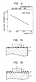
- Procédé pour fabriquer un dispositif à semiconducteurs comprenant :
la formation d'une pellicule de tungstène ou de molybdène (1) possédant une forme désirée sur un substrat en silicium (7), sur une pellicule (2) de SiO₂ disposée sur un substrat en silicium (3) ou sur une pellicule de siliciure de tungstène ou de molybdène (9) ; et
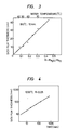
le chauffage de la structure résultante dans une atmosphère d'hydrogène contenant de la vapeur d'eau, le rapport entre les pressions partielles de la vapeur d'eau et du gaz hydrogène et la température de traitement thermique étant choisis en tant que valeurs entrant dans la zone comprise entre la courbe a et la courbe c de la figure 1 pour une pellicule de tungstène ou entrant dans la zone comprise entre la courbe b et la courbe c de la figure 1 pour une pellicule de molybdène, de manière à oxyder sélectivement la surface dudit substrat en silicium ou de ladite pellicule de siliciure sans oxyder des surfaces de ladite pellicule de tungstène ou de molybdène. - Procédé selon la revendication 1, selon lequel la température de traitement thermique se situe dans la gamme comprise entre environ 400°C et environ 1200°C.
- Procédé selon la revendication 1, selon lequel ledit substrat en silicium est un substrat en monocristal de silicium (3) ou un substrat en silicium polycristallin (7).
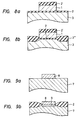
- Procédé pour fabriquer un dispositif à semiconducteurs selon la revendication 1, incluant les étapes comprenant
la formation d'une pellicule (2) de SiO₂ sur ledit substrat en silicium (3);
la formation de ladite pellicule de tungstène et de molybdène (1) avec la forme désirée sur ladite pellicule de SiO₂;
le dopage de la région superficielle dudit substrat en silicium avec une impureté possédant un type de conductivité opposé à celui dudit substrat en silicium (3), moyennant l'utilisation de ladite pellicule de tungstène ou de molybdène (1) en tant que masque; et
l'exécution dudit traitement thermique. - Procédé selon la revendication 4, selon lequel le dopage de ladite impureté est exécuté en déposant une pellicule stratifiée formant masque (2') comprenant au moins un élément incluant une pellicule de verre au phosphosilicate, une pellicule de SiO₂ et une pellicule de Si₃N₄ sur ladite pellicule de tungstène ou de molybdène (1), puis en effectuant une implantation ionique.
- Procédé selon la revendication 4, selon lequel ladite pellicule de tungstène ou de molybdène (1) est l'électrode de grille d'un dispositif à semiconducteurs à effet de champ MIS.
- Procédé selon la revendication 4, selon lequel ledit traitement thermique est effectué après l'élimination par attaque chimique d'une partie de ladite pellicule (2) de SiO₂, dans laquelle ladite pellicule de tungstène ou de molybdène (1) n'est pas déposée.
Applications Claiming Priority (2)
| Application Number | Priority Date | Filing Date | Title |
|---|---|---|---|
| JP6868/83 | 1983-01-19 | ||
| JP58006868A JPS59132136A (ja) | 1983-01-19 | 1983-01-19 | 半導体装置の製造方法 |
Publications (3)
| Publication Number | Publication Date |
|---|---|
| EP0116317A2 EP0116317A2 (fr) | 1984-08-22 |
| EP0116317A3 EP0116317A3 (en) | 1987-07-22 |
| EP0116317B1 true EP0116317B1 (fr) | 1992-04-01 |
Family
ID=11650210
Family Applications (1)
| Application Number | Title | Priority Date | Filing Date |
|---|---|---|---|
| EP84100507A Expired - Lifetime EP0116317B1 (fr) | 1983-01-19 | 1984-01-18 | Procédé pour la fabrication d'un dispositif semi-conducteur comportant une étape d'oxydation |
Country Status (5)
| Country | Link |
|---|---|
| US (1) | US4505028A (fr) |
| EP (1) | EP0116317B1 (fr) |
| JP (1) | JPS59132136A (fr) |
| KR (1) | KR910007097B1 (fr) |
| DE (1) | DE3485622D1 (fr) |
Cited By (1)
| Publication number | Priority date | Publication date | Assignee | Title |
|---|---|---|---|---|
| DE10236896A1 (de) * | 2002-08-12 | 2004-04-01 | Infineon Technologies Ag | Vorrichtung und Verfahren zum thermischen Behandeln von Halbleiterwafern |
Families Citing this family (36)
| Publication number | Priority date | Publication date | Assignee | Title |
|---|---|---|---|---|
| US4587710A (en) * | 1984-06-15 | 1986-05-13 | Gould Inc. | Method of fabricating a Schottky barrier field effect transistor |
| US5907188A (en) * | 1995-08-25 | 1999-05-25 | Kabushiki Kaisha Toshiba | Semiconductor device with conductive oxidation preventing film and method for manufacturing the same |
| US5789312A (en) * | 1996-10-30 | 1998-08-04 | International Business Machines Corporation | Method of fabricating mid-gap metal gates compatible with ultra-thin dielectrics |
| JPH10223900A (ja) * | 1996-12-03 | 1998-08-21 | Toshiba Corp | 半導体装置及び半導体装置の製造方法 |
| US6893980B1 (en) | 1996-12-03 | 2005-05-17 | Kabushiki Kaisha Toshiba | Semiconductor device and manufacturing method therefor |
| TWI278933B (en) | 1997-03-05 | 2007-04-11 | Hitachi Ltd | Method of making semiconductor IC device |
| JPH10335652A (ja) | 1997-05-30 | 1998-12-18 | Hitachi Ltd | 半導体集積回路装置の製造方法 |
| JPH10340909A (ja) | 1997-06-06 | 1998-12-22 | Hitachi Ltd | 半導体集積回路装置の製造方法 |
| US6159866A (en) * | 1998-03-02 | 2000-12-12 | Applied Materials, Inc. | Method for insitu vapor generation for forming an oxide on a substrate |
| JP4283904B2 (ja) | 1997-07-11 | 2009-06-24 | 株式会社東芝 | 半導体装置の製造方法 |
| US6037273A (en) * | 1997-07-11 | 2000-03-14 | Applied Materials, Inc. | Method and apparatus for insitu vapor generation |
| DE69840861D1 (de) * | 1997-10-14 | 2009-07-16 | Texas Instruments Inc | Verfahren zum Oxidieren einer Struktur während der Herstellung einer Halbleitervorrichtung |
| US6452276B1 (en) | 1998-04-30 | 2002-09-17 | International Business Machines Corporation | Ultra thin, single phase, diffusion barrier for metal conductors |
| JPH11330468A (ja) | 1998-05-20 | 1999-11-30 | Hitachi Ltd | 半導体集積回路装置の製造方法および半導体集積回路装置 |
| US6835672B1 (en) * | 1998-10-15 | 2004-12-28 | Texas Instruments Incorporated | Selective oxidation for semiconductor device fabrication |
| US6162694A (en) * | 1998-11-25 | 2000-12-19 | Advanced Micro Devices, Inc. | Method of forming a metal gate electrode using replaced polysilicon structure |
| DE19901210A1 (de) * | 1999-01-14 | 2000-07-27 | Siemens Ag | Halbleiterbauelement und Verfahren zu dessen Herstellung |
| JP2000349285A (ja) * | 1999-06-04 | 2000-12-15 | Hitachi Ltd | 半導体集積回路装置の製造方法および半導体集積回路装置 |
| TW434704B (en) * | 1999-06-11 | 2001-05-16 | Univ Nat Yunlin Sci & Tech | Device of amorphous WO3 ion sensitive field effect transistor (ISFET) and method for making the same |
| US6555407B1 (en) | 1999-10-26 | 2003-04-29 | Zarlink Semiconductor Ab | Method for the controlled oxidiation of materials |
| GB2355850A (en) * | 1999-10-26 | 2001-05-02 | Mitel Semiconductor Ab | Forming oxide layers in semiconductor layers |
| JP2001274154A (ja) | 2000-01-18 | 2001-10-05 | Applied Materials Inc | 成膜方法、成膜装置、半導体装置及びその製造方法 |
| US6603181B2 (en) * | 2001-01-16 | 2003-08-05 | International Business Machines Corporation | MOS device having a passivated semiconductor-dielectric interface |
| KR100650467B1 (ko) * | 2001-03-12 | 2006-11-28 | 가부시키가이샤 히타치세이사쿠쇼 | 반도체 집적 회로 장치 및 그 제조 방법 |
| WO2002073696A1 (fr) * | 2001-03-12 | 2002-09-19 | Hitachi, Ltd. | Procede pour fabriquer un dispositif semi-conducteur a circuit integre |
| KR100402389B1 (ko) * | 2001-03-23 | 2003-10-17 | 삼성전자주식회사 | 금속 게이트 형성 방법 |
| DE10120523A1 (de) | 2001-04-26 | 2002-10-31 | Infineon Technologies Ag | Verfahren zur Minimierung der Wolframoxidausdampfung bei der selektiven Seitenwandoxidation von Wolfram-Silizium-Gates |
| TW200416772A (en) * | 2002-06-06 | 2004-09-01 | Asml Us Inc | System and method for hydrogen-rich selective oxidation |
| KR100459725B1 (ko) * | 2002-09-19 | 2004-12-03 | 삼성전자주식회사 | 금속 게이트 패턴을 갖는 반도체소자의 제조방법 |
| JP2005101141A (ja) * | 2003-09-24 | 2005-04-14 | Renesas Technology Corp | 半導体集積回路装置およびその製造方法 |
| WO2005083795A1 (fr) * | 2004-03-01 | 2005-09-09 | Tokyo Electron Limited | Procédé de fabrication d’un dispositif semi-conducteur et procédé d’oxydation plasma |
| WO2006095752A1 (fr) * | 2005-03-08 | 2006-09-14 | Hitachi Kokusai Electric Inc. | Procede de fabrication de dispositifs semiconducteurs et dispositif de traitement de substrat |
| JP2007165788A (ja) * | 2005-12-16 | 2007-06-28 | Tokyo Electron Ltd | 金属系膜の脱炭素処理方法、成膜方法および半導体装置の製造方法 |
| US7951728B2 (en) | 2007-09-24 | 2011-05-31 | Applied Materials, Inc. | Method of improving oxide growth rate of selective oxidation processes |
| US9127340B2 (en) * | 2009-02-13 | 2015-09-08 | Asm International N.V. | Selective oxidation process |
| US8889565B2 (en) * | 2009-02-13 | 2014-11-18 | Asm International N.V. | Selective removal of oxygen from metal-containing materials |
Family Cites Families (5)
| Publication number | Priority date | Publication date | Assignee | Title |
|---|---|---|---|---|
| US3679492A (en) * | 1970-03-23 | 1972-07-25 | Ibm | Process for making mosfet's |
| NL164424C (nl) * | 1970-06-04 | 1980-12-15 | Philips Nv | Werkwijze voor het vervaardigen van een veldeffect- transistor met een geisoleerde stuurelektrode, waarbij een door een tegen oxydatie maskerende laag vrijgelaten deel van het oppervlak van een siliciumlichaam aan een oxydatiebehandeling wordt onderworpen ter verkrijging van een althans gedeeltelijk in het siliciumlichaam verzonken siliciumoxydelaag. |
| US3959025A (en) * | 1974-05-01 | 1976-05-25 | Rca Corporation | Method of making an insulated gate field effect transistor |
| US4093503A (en) * | 1977-03-07 | 1978-06-06 | International Business Machines Corporation | Method for fabricating ultra-narrow metallic lines |
| JPS5693314A (en) * | 1979-12-26 | 1981-07-28 | Fujitsu Ltd | Ion injector |
-
1983
- 1983-01-19 JP JP58006868A patent/JPS59132136A/ja active Granted
-
1984
- 1984-01-18 KR KR1019840000207A patent/KR910007097B1/ko not_active IP Right Cessation
- 1984-01-18 EP EP84100507A patent/EP0116317B1/fr not_active Expired - Lifetime
- 1984-01-18 DE DE8484100507T patent/DE3485622D1/de not_active Expired - Lifetime
- 1984-01-19 US US06/571,946 patent/US4505028A/en not_active Expired - Lifetime
Non-Patent Citations (1)
| Title |
|---|
| IEEE Transactions on Electron Devices, vol. ED-26, No. 4, April 1979, pages 369-371 * |
Cited By (2)
| Publication number | Priority date | Publication date | Assignee | Title |
|---|---|---|---|---|
| DE10236896A1 (de) * | 2002-08-12 | 2004-04-01 | Infineon Technologies Ag | Vorrichtung und Verfahren zum thermischen Behandeln von Halbleiterwafern |
| DE10236896B4 (de) * | 2002-08-12 | 2010-08-12 | Mattson Thermal Products Gmbh | Vorrichtung und Verfahren zum thermischen Behandeln von Halbleiterwafern |
Also Published As
| Publication number | Publication date |
|---|---|
| KR910007097B1 (ko) | 1991-09-18 |
| EP0116317A3 (en) | 1987-07-22 |
| EP0116317A2 (fr) | 1984-08-22 |
| JPH0458688B2 (fr) | 1992-09-18 |
| DE3485622D1 (de) | 1992-05-07 |
| JPS59132136A (ja) | 1984-07-30 |
| US4505028A (en) | 1985-03-19 |
| KR840007307A (ko) | 1984-12-06 |
Similar Documents
| Publication | Publication Date | Title |
|---|---|---|
| EP0116317B1 (fr) | Procédé pour la fabrication d'un dispositif semi-conducteur comportant une étape d'oxydation | |
| US4701349A (en) | Semiconductor integrated circuit device and method of producing the same | |
| EP1361614B1 (fr) | Procede de fabrication d'un dispositif semi-conducteur | |
| US5324974A (en) | Nitride capped MOSFET for integrated circuits | |
| US6727148B1 (en) | ULSI MOS with high dielectric constant gate insulator | |
| KR960013135B1 (ko) | 캡 산화물을 배치한 티탄 규화물 형성 방법 | |
| US6653700B2 (en) | Transistor structure and method of fabrication | |
| US5656546A (en) | Self-aligned tin formation by N2+ implantation during two-step annealing Ti-salicidation | |
| US5089432A (en) | Polycide gate MOSFET process for integrated circuits | |
| EP0617461A2 (fr) | Procédé pour la formation de couches diélectriques oxynitrides lors de la fabrication de circuits intégrés | |
| US20050130380A1 (en) | Semiconductor device structures including metal silicide interconnects and dielectric layers at substantially the same fabrication level | |
| JPS63316476A (ja) | 半導体装置およびその製造方法 | |
| JPH05211330A (ja) | 電界効果トランジスタおよびその製造方法 | |
| US5214305A (en) | Polycide gate MOSFET for integrated circuits | |
| US5130266A (en) | Polycide gate MOSFET process for integrated circuits | |
| US4551907A (en) | Process for fabricating a semiconductor device | |
| US5652183A (en) | Method for fabricating semiconductor device containing excessive silicon in metal silicide film | |
| US5288666A (en) | Process for forming self-aligned titanium silicide by heating in an oxygen rich environment | |
| US6444532B2 (en) | Process for fabricating MOS semiconductor transistor | |
| US7166525B2 (en) | High temperature hydrogen annealing of a gate insulator layer to increase etching selectivity between conductive gate structure and gate insulator layer | |
| JP3376158B2 (ja) | 半導体装置の製造方法 | |
| JPS62169412A (ja) | 半導体集積回路装置の製造方法 | |
| JP3185235B2 (ja) | 半導体装置の製造方法 | |
| US5108953A (en) | Method for fabricating a semiconductive device comprising a refractory metal silicide thin film | |
| JP2001015754A (ja) | 半導体素子の電導性ライン形成方法 |
Legal Events
| Date | Code | Title | Description |
|---|---|---|---|
| PUAI | Public reference made under article 153(3) epc to a published international application that has entered the european phase |
Free format text: ORIGINAL CODE: 0009012 |
|
| AK | Designated contracting states |
Designated state(s): DE FR GB IT |
|
| 17P | Request for examination filed |
Effective date: 19841220 |
|
| PUAL | Search report despatched |
Free format text: ORIGINAL CODE: 0009013 |
|
| AK | Designated contracting states |
Kind code of ref document: A3 Designated state(s): DE FR GB IT |
|
| 17Q | First examination report despatched |
Effective date: 19890905 |
|
| GRAA | (expected) grant |
Free format text: ORIGINAL CODE: 0009210 |
|
| AK | Designated contracting states |
Kind code of ref document: B1 Designated state(s): DE FR GB IT |
|
| PG25 | Lapsed in a contracting state [announced via postgrant information from national office to epo] |
Ref country code: IT Free format text: LAPSE BECAUSE OF FAILURE TO SUBMIT A TRANSLATION OF THE DESCRIPTION OR TO PAY THE FEE WITHIN THE PRESCRIBED TIME-LIMIT;WARNING: LAPSES OF ITALIAN PATENTS WITH EFFECTIVE DATE BEFORE 2007 MAY HAVE OCCURRED AT ANY TIME BEFORE 2007. THE CORRECT EFFECTIVE DATE MAY BE DIFFERENT FROM THE ONE RECORDED. Effective date: 19920401 Ref country code: FR Effective date: 19920401 |
|
| REF | Corresponds to: |
Ref document number: 3485622 Country of ref document: DE Date of ref document: 19920507 |
|
| EN | Fr: translation not filed | ||
| PLBE | No opposition filed within time limit |
Free format text: ORIGINAL CODE: 0009261 |
|
| STAA | Information on the status of an ep patent application or granted ep patent |
Free format text: STATUS: NO OPPOSITION FILED WITHIN TIME LIMIT |
|
| 26N | No opposition filed | ||
| REG | Reference to a national code |
Ref country code: GB Ref legal event code: IF02 |
|
| PGFP | Annual fee paid to national office [announced via postgrant information from national office to epo] |
Ref country code: GB Payment date: 20021223 Year of fee payment: 20 |
|
| PGFP | Annual fee paid to national office [announced via postgrant information from national office to epo] |
Ref country code: DE Payment date: 20030310 Year of fee payment: 20 |
|
| PG25 | Lapsed in a contracting state [announced via postgrant information from national office to epo] |
Ref country code: GB Free format text: LAPSE BECAUSE OF EXPIRATION OF PROTECTION Effective date: 20040117 |
|
| REG | Reference to a national code |
Ref country code: GB Ref legal event code: PE20 |