EP0094716B1 - Verfahren zur Verbindung eines Halbleiters mit Elementen eines Trägers, insbesondere einer tragbaren Karte - Google Patents
Verfahren zur Verbindung eines Halbleiters mit Elementen eines Trägers, insbesondere einer tragbaren Karte Download PDFInfo
- Publication number
- EP0094716B1 EP0094716B1 EP83200661A EP83200661A EP0094716B1 EP 0094716 B1 EP0094716 B1 EP 0094716B1 EP 83200661 A EP83200661 A EP 83200661A EP 83200661 A EP83200661 A EP 83200661A EP 0094716 B1 EP0094716 B1 EP 0094716B1
- Authority
- EP
- European Patent Office
- Prior art keywords
- chip
- metallizations
- support
- holes
- card
- Prior art date
- Legal status (The legal status is an assumption and is not a legal conclusion. Google has not performed a legal analysis and makes no representation as to the accuracy of the status listed.)
- Expired
Links
Images

Classifications
-
- G—PHYSICS
- G06—COMPUTING; CALCULATING OR COUNTING
- G06K—GRAPHICAL DATA READING; PRESENTATION OF DATA; RECORD CARRIERS; HANDLING RECORD CARRIERS
- G06K19/00—Record carriers for use with machines and with at least a part designed to carry digital markings
- G06K19/06—Record carriers for use with machines and with at least a part designed to carry digital markings characterised by the kind of the digital marking, e.g. shape, nature, code
- G06K19/067—Record carriers with conductive marks, printed circuits or semiconductor circuit elements, e.g. credit or identity cards also with resonating or responding marks without active components
- G06K19/07—Record carriers with conductive marks, printed circuits or semiconductor circuit elements, e.g. credit or identity cards also with resonating or responding marks without active components with integrated circuit chips
- G06K19/077—Constructional details, e.g. mounting of circuits in the carrier
- G06K19/07745—Mounting details of integrated circuit chips
-
- H—ELECTRICITY
- H01—ELECTRIC ELEMENTS
- H01L—SEMICONDUCTOR DEVICES NOT COVERED BY CLASS H10
- H01L24/00—Arrangements for connecting or disconnecting semiconductor or solid-state bodies; Methods or apparatus related thereto
- H01L24/01—Means for bonding being attached to, or being formed on, the surface to be connected, e.g. chip-to-package, die-attach, "first-level" interconnects; Manufacturing methods related thereto
- H01L24/18—High density interconnect [HDI] connectors; Manufacturing methods related thereto
- H01L24/23—Structure, shape, material or disposition of the high density interconnect connectors after the connecting process
- H01L24/24—Structure, shape, material or disposition of the high density interconnect connectors after the connecting process of an individual high density interconnect connector
-
- H—ELECTRICITY
- H01—ELECTRIC ELEMENTS
- H01L—SEMICONDUCTOR DEVICES NOT COVERED BY CLASS H10
- H01L24/00—Arrangements for connecting or disconnecting semiconductor or solid-state bodies; Methods or apparatus related thereto
- H01L24/80—Methods for connecting semiconductor or other solid state bodies using means for bonding being attached to, or being formed on, the surface to be connected
- H01L24/82—Methods for connecting semiconductor or other solid state bodies using means for bonding being attached to, or being formed on, the surface to be connected by forming build-up interconnects at chip-level, e.g. for high density interconnects [HDI]
-
- H—ELECTRICITY
- H01—ELECTRIC ELEMENTS
- H01L—SEMICONDUCTOR DEVICES NOT COVERED BY CLASS H10
- H01L2224/00—Indexing scheme for arrangements for connecting or disconnecting semiconductor or solid-state bodies and methods related thereto as covered by H01L24/00
- H01L2224/01—Means for bonding being attached to, or being formed on, the surface to be connected, e.g. chip-to-package, die-attach, "first-level" interconnects; Manufacturing methods related thereto
- H01L2224/02—Bonding areas; Manufacturing methods related thereto
- H01L2224/04—Structure, shape, material or disposition of the bonding areas prior to the connecting process
- H01L2224/04105—Bonding areas formed on an encapsulation of the semiconductor or solid-state body, e.g. bonding areas on chip-scale packages
-
- H—ELECTRICITY
- H01—ELECTRIC ELEMENTS
- H01L—SEMICONDUCTOR DEVICES NOT COVERED BY CLASS H10
- H01L2224/00—Indexing scheme for arrangements for connecting or disconnecting semiconductor or solid-state bodies and methods related thereto as covered by H01L24/00
- H01L2224/01—Means for bonding being attached to, or being formed on, the surface to be connected, e.g. chip-to-package, die-attach, "first-level" interconnects; Manufacturing methods related thereto
- H01L2224/18—High density interconnect [HDI] connectors; Manufacturing methods related thereto
- H01L2224/23—Structure, shape, material or disposition of the high density interconnect connectors after the connecting process
- H01L2224/24—Structure, shape, material or disposition of the high density interconnect connectors after the connecting process of an individual high density interconnect connector
- H01L2224/241—Disposition
- H01L2224/24151—Connecting between a semiconductor or solid-state body and an item not being a semiconductor or solid-state body, e.g. chip-to-substrate, chip-to-passive
- H01L2224/24221—Connecting between a semiconductor or solid-state body and an item not being a semiconductor or solid-state body, e.g. chip-to-substrate, chip-to-passive the body and the item being stacked
- H01L2224/24225—Connecting between a semiconductor or solid-state body and an item not being a semiconductor or solid-state body, e.g. chip-to-substrate, chip-to-passive the body and the item being stacked the item being non-metallic, e.g. insulating substrate with or without metallisation
- H01L2224/24227—Connecting between a semiconductor or solid-state body and an item not being a semiconductor or solid-state body, e.g. chip-to-substrate, chip-to-passive the body and the item being stacked the item being non-metallic, e.g. insulating substrate with or without metallisation the HDI interconnect not connecting to the same level of the item at which the semiconductor or solid-state body is mounted, e.g. the semiconductor or solid-state body being mounted in a cavity or on a protrusion of the item
-
- H—ELECTRICITY
- H01—ELECTRIC ELEMENTS
- H01L—SEMICONDUCTOR DEVICES NOT COVERED BY CLASS H10
- H01L2224/00—Indexing scheme for arrangements for connecting or disconnecting semiconductor or solid-state bodies and methods related thereto as covered by H01L24/00
- H01L2224/91—Methods for connecting semiconductor or solid state bodies including different methods provided for in two or more of groups H01L2224/80 - H01L2224/90
- H01L2224/92—Specific sequence of method steps
- H01L2224/921—Connecting a surface with connectors of different types
- H01L2224/9212—Sequential connecting processes
- H01L2224/92142—Sequential connecting processes the first connecting process involving a layer connector
- H01L2224/92144—Sequential connecting processes the first connecting process involving a layer connector the second connecting process involving a build-up interconnect
-
- H—ELECTRICITY
- H01—ELECTRIC ELEMENTS
- H01L—SEMICONDUCTOR DEVICES NOT COVERED BY CLASS H10
- H01L2924/00—Indexing scheme for arrangements or methods for connecting or disconnecting semiconductor or solid-state bodies as covered by H01L24/00
- H01L2924/01—Chemical elements
- H01L2924/01005—Boron [B]
-
- H—ELECTRICITY
- H01—ELECTRIC ELEMENTS
- H01L—SEMICONDUCTOR DEVICES NOT COVERED BY CLASS H10
- H01L2924/00—Indexing scheme for arrangements or methods for connecting or disconnecting semiconductor or solid-state bodies as covered by H01L24/00
- H01L2924/01—Chemical elements
- H01L2924/01006—Carbon [C]
-
- H—ELECTRICITY
- H01—ELECTRIC ELEMENTS
- H01L—SEMICONDUCTOR DEVICES NOT COVERED BY CLASS H10
- H01L2924/00—Indexing scheme for arrangements or methods for connecting or disconnecting semiconductor or solid-state bodies as covered by H01L24/00
- H01L2924/01—Chemical elements
- H01L2924/01015—Phosphorus [P]
-
- H—ELECTRICITY
- H01—ELECTRIC ELEMENTS
- H01L—SEMICONDUCTOR DEVICES NOT COVERED BY CLASS H10
- H01L2924/00—Indexing scheme for arrangements or methods for connecting or disconnecting semiconductor or solid-state bodies as covered by H01L24/00
- H01L2924/01—Chemical elements
- H01L2924/01032—Germanium [Ge]
-
- H—ELECTRICITY
- H01—ELECTRIC ELEMENTS
- H01L—SEMICONDUCTOR DEVICES NOT COVERED BY CLASS H10
- H01L2924/00—Indexing scheme for arrangements or methods for connecting or disconnecting semiconductor or solid-state bodies as covered by H01L24/00
- H01L2924/01—Chemical elements
- H01L2924/01033—Arsenic [As]
-
- H—ELECTRICITY
- H01—ELECTRIC ELEMENTS
- H01L—SEMICONDUCTOR DEVICES NOT COVERED BY CLASS H10
- H01L2924/00—Indexing scheme for arrangements or methods for connecting or disconnecting semiconductor or solid-state bodies as covered by H01L24/00
- H01L2924/01—Chemical elements
- H01L2924/01039—Yttrium [Y]
-
- H—ELECTRICITY
- H01—ELECTRIC ELEMENTS
- H01L—SEMICONDUCTOR DEVICES NOT COVERED BY CLASS H10
- H01L2924/00—Indexing scheme for arrangements or methods for connecting or disconnecting semiconductor or solid-state bodies as covered by H01L24/00
- H01L2924/01—Chemical elements
- H01L2924/01052—Tellurium [Te]
-
- H—ELECTRICITY
- H01—ELECTRIC ELEMENTS
- H01L—SEMICONDUCTOR DEVICES NOT COVERED BY CLASS H10
- H01L2924/00—Indexing scheme for arrangements or methods for connecting or disconnecting semiconductor or solid-state bodies as covered by H01L24/00
- H01L2924/01—Chemical elements
- H01L2924/01057—Lanthanum [La]
-
- H—ELECTRICITY
- H01—ELECTRIC ELEMENTS
- H01L—SEMICONDUCTOR DEVICES NOT COVERED BY CLASS H10
- H01L2924/00—Indexing scheme for arrangements or methods for connecting or disconnecting semiconductor or solid-state bodies as covered by H01L24/00
- H01L2924/01—Chemical elements
- H01L2924/01058—Cerium [Ce]
-
- H—ELECTRICITY
- H01—ELECTRIC ELEMENTS
- H01L—SEMICONDUCTOR DEVICES NOT COVERED BY CLASS H10
- H01L2924/00—Indexing scheme for arrangements or methods for connecting or disconnecting semiconductor or solid-state bodies as covered by H01L24/00
- H01L2924/01—Chemical elements
- H01L2924/01078—Platinum [Pt]
-
- H—ELECTRICITY
- H01—ELECTRIC ELEMENTS
- H01L—SEMICONDUCTOR DEVICES NOT COVERED BY CLASS H10
- H01L2924/00—Indexing scheme for arrangements or methods for connecting or disconnecting semiconductor or solid-state bodies as covered by H01L24/00
- H01L2924/01—Chemical elements
- H01L2924/01079—Gold [Au]
-
- H—ELECTRICITY
- H01—ELECTRIC ELEMENTS
- H01L—SEMICONDUCTOR DEVICES NOT COVERED BY CLASS H10
- H01L2924/00—Indexing scheme for arrangements or methods for connecting or disconnecting semiconductor or solid-state bodies as covered by H01L24/00
- H01L2924/013—Alloys
- H01L2924/0132—Binary Alloys
- H01L2924/01327—Intermediate phases, i.e. intermetallics compounds
-
- H—ELECTRICITY
- H01—ELECTRIC ELEMENTS
- H01L—SEMICONDUCTOR DEVICES NOT COVERED BY CLASS H10
- H01L2924/00—Indexing scheme for arrangements or methods for connecting or disconnecting semiconductor or solid-state bodies as covered by H01L24/00
- H01L2924/013—Alloys
- H01L2924/014—Solder alloys
-
- H—ELECTRICITY
- H01—ELECTRIC ELEMENTS
- H01L—SEMICONDUCTOR DEVICES NOT COVERED BY CLASS H10
- H01L2924/00—Indexing scheme for arrangements or methods for connecting or disconnecting semiconductor or solid-state bodies as covered by H01L24/00
- H01L2924/095—Indexing scheme for arrangements or methods for connecting or disconnecting semiconductor or solid-state bodies as covered by H01L24/00 with a principal constituent of the material being a combination of two or more materials provided in the groups H01L2924/013 - H01L2924/0715
- H01L2924/097—Glass-ceramics, e.g. devitrified glass
- H01L2924/09701—Low temperature co-fired ceramic [LTCC]
-
- H—ELECTRICITY
- H01—ELECTRIC ELEMENTS
- H01L—SEMICONDUCTOR DEVICES NOT COVERED BY CLASS H10
- H01L2924/00—Indexing scheme for arrangements or methods for connecting or disconnecting semiconductor or solid-state bodies as covered by H01L24/00
- H01L2924/10—Details of semiconductor or other solid state devices to be connected
- H01L2924/11—Device type
- H01L2924/12—Passive devices, e.g. 2 terminal devices
- H01L2924/1203—Rectifying Diode
- H01L2924/12033—Gunn diode
-
- H—ELECTRICITY
- H01—ELECTRIC ELEMENTS
- H01L—SEMICONDUCTOR DEVICES NOT COVERED BY CLASS H10
- H01L2924/00—Indexing scheme for arrangements or methods for connecting or disconnecting semiconductor or solid-state bodies as covered by H01L24/00
- H01L2924/10—Details of semiconductor or other solid state devices to be connected
- H01L2924/11—Device type
- H01L2924/12—Passive devices, e.g. 2 terminal devices
- H01L2924/1204—Optical Diode
- H01L2924/12042—LASER
-
- H—ELECTRICITY
- H01—ELECTRIC ELEMENTS
- H01L—SEMICONDUCTOR DEVICES NOT COVERED BY CLASS H10
- H01L2924/00—Indexing scheme for arrangements or methods for connecting or disconnecting semiconductor or solid-state bodies as covered by H01L24/00
- H01L2924/10—Details of semiconductor or other solid state devices to be connected
- H01L2924/11—Device type
- H01L2924/14—Integrated circuits
-
- H—ELECTRICITY
- H01—ELECTRIC ELEMENTS
- H01L—SEMICONDUCTOR DEVICES NOT COVERED BY CLASS H10
- H01L2924/00—Indexing scheme for arrangements or methods for connecting or disconnecting semiconductor or solid-state bodies as covered by H01L24/00
- H01L2924/19—Details of hybrid assemblies other than the semiconductor or other solid state devices to be connected
- H01L2924/1901—Structure
- H01L2924/1904—Component type
- H01L2924/19042—Component type being an inductor
-
- Y—GENERAL TAGGING OF NEW TECHNOLOGICAL DEVELOPMENTS; GENERAL TAGGING OF CROSS-SECTIONAL TECHNOLOGIES SPANNING OVER SEVERAL SECTIONS OF THE IPC; TECHNICAL SUBJECTS COVERED BY FORMER USPC CROSS-REFERENCE ART COLLECTIONS [XRACs] AND DIGESTS
- Y10—TECHNICAL SUBJECTS COVERED BY FORMER USPC
- Y10S—TECHNICAL SUBJECTS COVERED BY FORMER USPC CROSS-REFERENCE ART COLLECTIONS [XRACs] AND DIGESTS
- Y10S283/00—Printed matter
- Y10S283/904—Credit card
Definitions
- the invention relates to a method for making an electrical connection between metallizations of a semiconductor circuit chip and conductive tracks, possibly metallic, carried by a first face of a thin support, according to which one realizes in the thin support holes with a configuration corresponding to that of the metallizations on the patch, and, the second face of said thin support being entirely insulating, the patch is applied to this second face with its metallizations turned towards this second face, in correspondence with said holes.
- the method according to the invention advantageously applies to the production of a portable card containing a semiconductor circuit, in particular a payment card or an identity card, offering flat conductive elements, consisting of a conductive paste, connected at the terminals of the semiconductor circuit to allow an electrical connection with an external member, and in the material of which the semiconductor circuit is directly included in the form of a semiconductor wafer, the terminals of which are formed by metallizations.
- the thin supports used in the invention are used in the electronics industry to transfer a semiconductor wafer onto a complex electronic circuit, ensuring mechanical strength at the same time as the electrical interconnection of the wafer.
- semiconductor circuit chip or in abbreviated form “semiconductor chip”, is meant here one of the elements obtained by cutting wafers of semiconductor material, on which integrated circuits have been produced (these elements are commonly designated in the jargon of the skilled person under the name of "chips").
- One solution for transferring a pellet into a circuit consists in using a film which is kept in the finished product, and which provides isolation from the edges of the pellet by its location between the ribbon or conductive track located on one side, and the patch on the other side.
- a solution is described by an article in the review "Electronique Industrielle", of May 1, 1981, pages 87-88. It uses a 25 micron polyimide support, the conductive tracks of which are connected by metallized holes to other conductive tracks situated on the other face, themselves welded to the metallizations of the patch.
- the essential object of the present invention is to provide a process according to which quality devices can be obtained for an extremely low cost price. Because of this low cost price, the method can be applied to the production of mass-market devices such as portable cards, of the payment card or identity card type. It can also be applied to mounting brackets for integrated circuits which can be used in economical assemblies, and more particularly when a reduced bulk is required, such as in watches or pocket calculators.
- the general inventive concept of the invention results from the idea that it is possible to establish an electrical contact between a metallization of the patch and a conductive track located on the other face of the thin support, by filling the hole with a conductive paste which overflows on the conductive track. Or on the side of the tablet, on the contrary, the paste cannot overflow the hole since the tablet is applied against the support.
- This is one of the notable advantages of the invention compared to certain conventional solutions, such as the transfer of "face down" tablets, with glued contacts.
- the method according to the invention is notably remarkable in that the support being previously provided, in a known manner, with conductive tracks, arranged so as to comprise portions at the edge of said holes, the tablet and the support applied are maintained. one against the other while depositing, from the first face, an island of conductive paste on each hole so as to cover both the metallization and the conductive track.
- the method according to the invention is notably remarkable in that, said thin support being initially entirely insulating, the tablet applied to one face of the support while the tracks are formed on the face opposite to that carrying the pastille by means of a conductive paste give them a configuration such that portions of tracks cover the holes so that the paste penetrates therein, thus coming into contact with the metallizations of the patch.
- This process is ideally simple, and can be applied to a non-metallized support beforehand. It is therefore particularly economical.
- the method according to the invention is advantageously used to produce a portable card offering flat conductive elements connected to the terminals of a semiconductor circuit included directly in the form of a chip in the material of the card, and is therefore notably remarkable.
- said pellet is placed very close to one face of the card with its metallizations facing said face, thus constituting a thin wall opposite the pellet in that holes are made in this thin wall, in look at the metallizations of the wafer, and in that, finally, at the same time as the above-mentioned flat conductive elements are formed, the conductive paste is made to extend from each conductive element until the associated metallization of the wafer, by making it penetrate into the holes.
- the card constitutes by itself the aforementioned "thin support", which provides remarkable simplicity of construction and a particularly low cost price.
- Figure 4 shows in section a device similar to that of Figure 2, obtained by a variant of the method according to the invention.
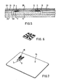
- FIG. 5 represents in section a portable card obtained by the method according to the invention.
- Figures 6 and 7 show in perspective examples of devices obtained by the method according to the invention.
- FIG. 1 represents a semiconductor circuit chip 5, provided with metallizations 3, and a thin support 2 provided with metallic conductive tracks 1 carried by a first face 8 of this thin support.
- holes 4 are made with a configuration corresponding to that of the metallizations 3 on the patch.
- the holes in the support are arranged in such a way that by applying the tablet against the support with an adequate positioning, there is a hole in the support opposite each metallization of the tablet.
- the conductive tracks 1 are arranged so as to comprise portions at the edge of the holes. Preferably, these portions bordering the holes are formed by rings surrounding the holes, usually called lunules.
- the support and the tracks consist of a conventional thin printed circuit, called "single-sided", on which a large number of pads are mounted, and which are cut into small pieces each containing either a pad or several interconnected pads.
- the support can also be constituted by a film in the form of a ribbon possibly provided with positioning holes and carrying metal tracks deposited on one of its faces.
- This film provided with pellets by the method of the invention, and wound on a reel, is used in a machine which cuts it and transfers onto electronic circuits portions of film each provided with a tablet.
- the thickness H of the support should be relatively small compared to the dimension of the holes, the latter being of the same order of magnitude as that of the metallizations: a thickness H of less than 0.3 mm is preferably used.
- the metallizations 3 of the patch are slightly larger. For example, they can have a width A of 0.5 mm. This is a noticeably larger dimension than is customary with regard to integrated circuits. It should be noted that the invention preferably applies to integrated circuits having a great complexity, but nevertheless comprising a reduced number of input / output metallizations. This is the case, for example, for circuits used for payment cards, which offer multiple and complex logic functions and have only eight or even only six terminals. Suppose for example that a chip bearing such a circuit has a surface of 15 mm2 with six metallizations of 0.1 mm x 0.1 mm.
- the patch 5 is placed on this second face 7 with its metallizations 3 facing this second face and in correspondence with the holes 4 and, as shown in FIG. 2, an island of polymerizable conductive paste 6 is deposited from the first face 8 on each hole so as to cover both the metallization placed under the hole and the conductive track 1 at the edge of said hole.
- This paste is then preferably brought in using a screen or a stencil and a squeegee.
- the screen is for example made of a fabric covered with a coating photo-etched in the well-known process known as: screen printing.
- the tablet and the support are held in place during the deposition of the dough by known mechanical means, for example a plate provided with holes and a suction, as a result of which the viscosity and the adhesion of the dough are sufficient to maintain the pellet during subsequent manipulations until the polymerization of the dough has been ensured, for example by heating in an oven.
- the metallizations of the tablet preferably consist of a titanium / platinum / gold stack which gives good results with most commercially available conductive pastes.
- the pellet can also be maintained thanks to a shim 17, of thickness equal to, or slightly less than that of the pellet 5.
- a wall (not shown) is fixed to the interior face of the device and keeps the tablet in place, at least during the deposition and, if necessary, the polymerization of the conductive material 6.
- This wall can, for example, be made of adhesive tape .
- the pellet can also be held by a bead of suitable material deposited along the perimeter of the pellet, between the latter and the shim 17.
- a material can be a polymerizable insulating paste or a glass fusible at low temperature. This arrangement has the advantage of subsequently providing climatic protection of the pellet.
- the wedge 17 can be bonded to the support 2, for example according to a known method of pressing multilayer printed circuits.
- This support can also be made of ceramic, which has several advantages: the recess can then be obtained, as well as the holes, directly by molding, and it can be used, to ensure the best possible seal along the perimeter of the pellet, a glass fusible at a temperature up to 300 to 400 ° C. the various expansion coefficients (silicon, glass, ceramic) being well tuned.
- a fully insulating support is used, as shown in 2 in FIG. 4, the patch 5 is placed on one face 7 of this support, with its metallizations 3 facing this face and in correspondence with the holes 4, and the tracks 9 are then formed on the other face by means of a conductive paste, giving them a configuration such that portions of tracks cover the holes 4 so that the paste penetrates therefrom, thus in contact with the metallizations 3 of the patch.
- These tracks 9 are preferably deposited by means of a screen printing.
- FIG. 3 represents portions of wafer 5 with metallizations 3. On each metallization, a portion of metal wire has been welded, before cutting the slices of semiconductor material supplying the pellets. To the left of the figure, a wire 12 has been welded at two neighboring points on the same metallization, thereby forming a sort of basket handle which improves the attachment of the conductive material to the metallization. It must be understood, however, that these arrangements, which are only intended to obtain better efficiency and better reliability, are not essential for the implementation of the invention.
- the product to be produced is a portable electronic card, as indicated in the preamble, it is advantageously possible, instead of including a support in the card, to produce the latter in such a way that it constitutes it even directly the support of the integrated circuit chip.
- Such a card offers flat conductive elements (10, FIG. 7) which serve to establish electrical contacts with a device by means of which the card is operated.
- These flat conductive elements can be produced by means of a conductive paste, and must be joined at the terminals of the semiconductor circuit included directly in the card.
- FIG. 5 represents stacked sheets 21, 22, 23, 24.
- the central sheets 22, 23 have a thickness substantially equal to that of the pellet 5.
- the two outer layers 21 and 24 allow the pellet 5 to be enclosed in the assembly. Once this stack is hot pressed with the pad 5 inside, it is placed very close to one face of the card, here the upper face, with its metallizations 3 facing towards said face. A thin wall 20 has therefore been formed in front of the patch. Holes 4 have been made in this thin wall, prior to pressing the stack, and placed the sheet 21 so that these holes are facing the metallizations 3 of the pellet.
- the sheets 21 to 24 constituting the card can be made of polyvinyl chloride, called PVC, and pressed according to the usual technique of manufacturing portable cards with magnetic tracks.
- They can also be made of laminated fiberglass and epoxy, such as that used for making multilayer printed circuits, and pressed according to the known technique of these circuits. It is also possible to produce the assembly corresponding to the sheets 21, 22, 23 in one piece, for example by molding it with one of the many materials capable of being transfer molded. The holes 4 will then come from molding. The patch 5 will then be put in place, for example glued to the sheet 24, and the latter in turn glued to the assembly 21, 22, 23.
- the above-mentioned flat conductive elements are formed by screen printing of a conductive paste at low polymerization temperature, and at the same time as these elements are formed, extend the conductive paste from each element to the associated metallization of the pellet, making it penetrate into the holes: thus the design of the conductors formed by screen printing is such that a single pattern constitutes a above-mentioned flat conductive element and a conductive track connecting it to the integrated circuit chip, and each track covers a hole so that its material penetrates there and makes contact with a metallization of the chip.
- a protective sheet 11 can finally be glued to the stack to protect the tracks 9 and the flat conductive elements.
- orifices are provided in this sheet 11 to give access to the flat conductors.
- FIG. 6 represents an integrated circuit support produced according to the method of the invention and intended to be used in an electronic sub-assembly, or also to be included in a portable card.
- FIG. 7 which represents a portable card directly constituting the support of an integrated circuit chip makes it possible to appreciate the configuration of the conductors.
- the above flat conductive elements are represented at 10, the tracks at 9. These end in rounded studs above each hole to make contact with the "buried" patch, the position of which is indicated by arrow 5.
- the method according to the invention deserves to be used in a so-called “multiple” manufacturing process, that is to say that a plate or a strip is produced containing a large number of devices such as those of FIGS. 6 or 7, and that the plates or the strips are entirely cut at the end in order to obtain individual devices.
Claims (4)
Applications Claiming Priority (2)
| Application Number | Priority Date | Filing Date | Title |
|---|---|---|---|
| FR8208430 | 1982-05-14 | ||
| FR8208430A FR2527036A1 (fr) | 1982-05-14 | 1982-05-14 | Procede pour connecter un semiconducteur a des elements d'un support, notamment d'une carte portative |
Publications (2)
| Publication Number | Publication Date |
|---|---|
| EP0094716A1 EP0094716A1 (de) | 1983-11-23 |
| EP0094716B1 true EP0094716B1 (de) | 1987-01-14 |
Family
ID=9274042
Family Applications (1)
| Application Number | Title | Priority Date | Filing Date |
|---|---|---|---|
| EP83200661A Expired EP0094716B1 (de) | 1982-05-14 | 1983-05-06 | Verfahren zur Verbindung eines Halbleiters mit Elementen eines Trägers, insbesondere einer tragbaren Karte |
Country Status (6)
| Country | Link |
|---|---|
| US (1) | US4731645A (de) |
| EP (1) | EP0094716B1 (de) |
| JP (1) | JPS58209133A (de) |
| CA (1) | CA1201821A (de) |
| DE (1) | DE3369233D1 (de) |
| FR (1) | FR2527036A1 (de) |
Cited By (1)
| Publication number | Priority date | Publication date | Assignee | Title |
|---|---|---|---|---|
| DE3805130A1 (de) * | 1987-02-20 | 1988-09-01 | Mitsubishi Electric Corp | Gehaeuse fuer eine halbleiteranordnung |
Families Citing this family (62)
| Publication number | Priority date | Publication date | Assignee | Title |
|---|---|---|---|---|
| FR2555744B1 (fr) * | 1983-11-30 | 1986-05-09 | Philips Ind Commerciale | Eprouvette avec moyens de memorisation des resultats d'analyse |
| DE3485776T2 (de) * | 1983-12-06 | 1992-12-24 | Mars Inc | Marken und vorrichtung zur markenverarbeitung. |
| JPH0815187B2 (ja) * | 1984-02-17 | 1996-02-14 | 株式会社東芝 | 集積回路装置の製造方法 |
| JPS6146736U (ja) * | 1984-08-31 | 1986-03-28 | カシオ計算機株式会社 | 半導体チツプの取付構造 |
| CH661808A5 (fr) * | 1985-01-21 | 1987-08-14 | Lupa Finances | Carte munie d'un microprocesseur et/ou d'au moins une memoire electronique. |
| JPH0751390B2 (ja) * | 1985-07-10 | 1995-06-05 | カシオ計算機株式会社 | Icカ−ド |
| US4889980A (en) * | 1985-07-10 | 1989-12-26 | Casio Computer Co., Ltd. | Electronic memory card and method of manufacturing same |
| JPH074995B2 (ja) * | 1986-05-20 | 1995-01-25 | 株式会社東芝 | Icカ−ド及びその製造方法 |
| DE3639630A1 (de) * | 1986-11-20 | 1988-06-01 | Gao Ges Automation Org | Datentraeger mit integriertem schaltkreis und verfahren zur herstellung desselben |
| JPS63149191A (ja) * | 1986-12-15 | 1988-06-21 | 日立マクセル株式会社 | Icカ−ド |
| JP2579937B2 (ja) * | 1987-04-15 | 1997-02-12 | 株式会社東芝 | 電子回路装置およびその製造方法 |
| FR2635916B1 (fr) * | 1988-08-23 | 1990-10-12 | Bull Sa | Support de circuit integre de haute densite et son procede de fabrication |
| US6938825B1 (en) | 1989-04-24 | 2005-09-06 | Ultracard, Inc. | Data system |
| US5107099A (en) * | 1989-04-24 | 1992-04-21 | Smith Malcolm G | Magnetic card reader and method |
| US5157244A (en) * | 1989-12-19 | 1992-10-20 | Amp Incorporated | Smart key system |
| JPH0463282U (de) * | 1990-10-04 | 1992-05-29 | ||
| EP0569401A1 (de) * | 1991-01-28 | 1993-11-18 | Siemens Aktiengesellschaft | Verfahren zur herstellung einer tragbaren datenträgeranordnung |
| JP2816028B2 (ja) * | 1991-02-18 | 1998-10-27 | 株式会社東芝 | 半導体装置の製造方法 |
| US5422514A (en) * | 1993-05-11 | 1995-06-06 | Micromodule Systems, Inc. | Packaging and interconnect system for integrated circuits |
| DE4325458A1 (de) * | 1993-07-29 | 1995-02-09 | Orga Bond Technik Gmbh | Trägerelement für einen IC-Baustein |
| FR2721732B1 (fr) * | 1994-06-22 | 1996-08-30 | Solaic Sa | Carte à mémoire sans contact dont le circuit électronique comporte un module. |
| DE19539181C2 (de) * | 1995-10-20 | 1998-05-14 | Ods Gmbh & Co Kg | Chipkartenmodul sowie entsprechendes Herstellungsverfahren |
| US6013948A (en) * | 1995-11-27 | 2000-01-11 | Micron Technology, Inc. | Stackable chip scale semiconductor package with mating contacts on opposed surfaces |
| US5674785A (en) * | 1995-11-27 | 1997-10-07 | Micron Technology, Inc. | Method of producing a single piece package for semiconductor die |
| US6861290B1 (en) * | 1995-12-19 | 2005-03-01 | Micron Technology, Inc. | Flip-chip adaptor package for bare die |
| US5811879A (en) * | 1996-06-26 | 1998-09-22 | Micron Technology, Inc. | Stacked leads-over-chip multi-chip module |
| JP2777114B2 (ja) * | 1996-09-02 | 1998-07-16 | 株式会社日立製作所 | テープキャリア |
| US6250192B1 (en) * | 1996-11-12 | 2001-06-26 | Micron Technology, Inc. | Method for sawing wafers employing multiple indexing techniques for multiple die dimensions |
| DE19735171A1 (de) * | 1997-08-13 | 1999-01-07 | Siemens Ag | Halbleitermodul |
| US5899705A (en) * | 1997-11-20 | 1999-05-04 | Akram; Salman | Stacked leads-over chip multi-chip module |
| DE19809073A1 (de) * | 1998-03-04 | 1999-09-16 | Orga Kartensysteme Gmbh | Chipmodul und Verfahren zur Herstellung einer Chipkarte |
| EP0942392A3 (de) * | 1998-03-13 | 2000-10-18 | Kabushiki Kaisha Toshiba | Chipkarte |
| USRE43112E1 (en) | 1998-05-04 | 2012-01-17 | Round Rock Research, Llc | Stackable ball grid array package |
| US6414391B1 (en) | 1998-06-30 | 2002-07-02 | Micron Technology, Inc. | Module assembly for stacked BGA packages with a common bus bar in the assembly |
| DE19830540A1 (de) * | 1998-07-08 | 2000-01-13 | Siemens Ag | Elektronischer Schaltungsträger |
| US6871787B1 (en) | 1998-07-10 | 2005-03-29 | Ultracard, Inc. | Data storage card having a glass substrate and data surface region and method for using same |
| JP2000099678A (ja) * | 1998-09-18 | 2000-04-07 | Hitachi Ltd | Icカード及びその製造方法 |
| DE19845665C2 (de) * | 1998-10-05 | 2000-08-17 | Orga Kartensysteme Gmbh | Verfahren zur Herstellung eines Trägerelements für einen IC-Baustein zum Einbau in Chipkarten |
| US6815251B1 (en) | 1999-02-01 | 2004-11-09 | Micron Technology, Inc. | High density modularity for IC's |
| DE19940480C2 (de) | 1999-08-26 | 2001-06-13 | Orga Kartensysteme Gmbh | Leiterbahnträgerschicht zur Einlaminierung in eine Chipkarte, Chipkarte mit einer Leiterbahnträgerschicht und Verfahren zur Herstellung einer Chipkarte |
| US7487908B1 (en) | 1999-10-23 | 2009-02-10 | Ultracard, Inc. | Article having an embedded accessible storage member, apparatus and method for using same |
| US8397998B1 (en) | 1999-10-23 | 2013-03-19 | Ultracard, Inc. | Data storage device, apparatus and method for using same |
| US7036739B1 (en) | 1999-10-23 | 2006-05-02 | Ultracard, Inc. | Data storage device apparatus and method for using same |
| DE19955538B4 (de) * | 1999-11-18 | 2014-06-05 | Morpho Cards Gmbh | Leiterbahnträgerschicht zur Einlaminierung in eine Chipkarte, Verfahren zur Herstellung einer Leiterbahnträgerschicht Spritzgusswerkzeug zur Durchführung des Verfahrens zur Herstellung einer Leiterbahnträgerschicht |
| DE10014379A1 (de) * | 2000-03-23 | 2001-10-11 | Infineon Technologies Ag | Verfahren und Vorrichtung zum Verbinden mindestens eines Chips mit einer Umverdrahtungsanordnung |
| DE10042312A1 (de) * | 2000-08-29 | 2002-03-14 | Orga Kartensysteme Gmbh | Verfahren zur Herstellung eines Trägerelementes für einen IC-Baustein |
| US6969006B1 (en) | 2000-09-15 | 2005-11-29 | Ultracard, Inc. | Rotable portable card having a data storage device, apparatus and method for using same |
| US6707149B2 (en) * | 2000-09-29 | 2004-03-16 | Tessera, Inc. | Low cost and compliant microelectronic packages for high i/o and fine pitch |
| FR2816107B1 (fr) * | 2000-10-30 | 2003-11-28 | Gemplus Card Int | Module de circuit integre sur film et son procede de fabrication |
| FR2818802B1 (fr) * | 2000-12-21 | 2003-11-28 | Gemplus Card Int | Connexion par isolant decoupe et cordon imprime en plan |
| FR2822338B1 (fr) * | 2001-03-14 | 2003-06-27 | Sagem | Procede pour connecter electriquement des plots de contact d'un composant microelectronique directement a des pistes de circuits imprimes, et plaque a circuits imprimes ainsi constituee |
| JP3678212B2 (ja) * | 2002-05-20 | 2005-08-03 | ウシオ電機株式会社 | 超高圧水銀ランプ |
| US6755700B2 (en) * | 2002-11-12 | 2004-06-29 | Modevation Enterprises Inc. | Reset speed control for watercraft |
| US20040102753A1 (en) * | 2002-11-26 | 2004-05-27 | Kimberly-Clark Worldwide, Inc. | Male incontinence absorbent article and method of producing same |
| FI20031341A (fi) | 2003-09-18 | 2005-03-19 | Imbera Electronics Oy | Menetelmä elektroniikkamoduulin valmistamiseksi |
| FI117814B (fi) * | 2004-06-15 | 2007-02-28 | Imbera Electronics Oy | Menetelmä elektroniikkamoduulin valmistamiseksi |
| US8225499B2 (en) * | 2005-06-16 | 2012-07-24 | Imbera Electronics Oy | Method for manufacturing a circuit board structure, and a circuit board structure |
| FI119714B (fi) | 2005-06-16 | 2009-02-13 | Imbera Electronics Oy | Piirilevyrakenne ja menetelmä piirilevyrakenteen valmistamiseksi |
| FI122128B (fi) * | 2005-06-16 | 2011-08-31 | Imbera Electronics Oy | Menetelmä piirilevyrakenteen valmistamiseksi |
| US10206288B2 (en) * | 2015-08-13 | 2019-02-12 | Palo Alto Research Center Incorporated | Bare die integration with printed components on flexible substrate |
| US10165677B2 (en) | 2015-12-10 | 2018-12-25 | Palo Alto Research Center Incorporated | Bare die integration with printed components on flexible substrate without laser cut |
| US10847384B2 (en) | 2017-05-31 | 2020-11-24 | Palo Alto Research Center Incorporated | Method and fixture for chip attachment to physical objects |
Family Cites Families (12)
| Publication number | Priority date | Publication date | Assignee | Title |
|---|---|---|---|---|
| DE2202348A1 (de) * | 1972-01-19 | 1973-07-26 | Siemens Ag | Kreuzschienenverteiler |
| JPS5180770A (de) * | 1975-01-13 | 1976-07-14 | Suwa Seikosha Kk | |
| GB1565207A (en) * | 1975-09-05 | 1980-04-16 | Sinclair Radionics | Printed circuits |
| US4222516A (en) * | 1975-12-31 | 1980-09-16 | Compagnie Internationale Pour L'informatique Cii-Honeywell Bull | Standardized information card |
| FR2382101A1 (fr) * | 1977-02-28 | 1978-09-22 | Labo Electronique Physique | Dispositif a semi-conducteur, comportant des pattes metalliques isolees |
| US4246595A (en) * | 1977-03-08 | 1981-01-20 | Matsushita Electric Industrial Co., Ltd. | Electronics circuit device and method of making the same |
| DE2920012B1 (de) * | 1979-05-17 | 1980-11-20 | Gao Ges Automation Org | Ausweiskarte mit IC-Baustein und Verfahren zur Herstellung einer derartigen Ausweiskarte |
| JPS5649178U (de) * | 1979-09-21 | 1981-05-01 | ||
| US4544989A (en) * | 1980-06-30 | 1985-10-01 | Sharp Kabushiki Kaisha | Thin assembly for wiring substrate |
| FR2490059A1 (fr) * | 1980-09-09 | 1982-03-12 | Serras Paulet Edouard | Circuit imprime et son procede de fabrication |
| US4549247A (en) * | 1980-11-21 | 1985-10-22 | Gao Gesellschaft Fur Automation Und Organisation Mbh | Carrier element for IC-modules |
| DE3153768C2 (de) * | 1981-04-14 | 1995-11-09 | Gao Ges Automation Org | Ausweiskarte |
-
1982
- 1982-05-14 FR FR8208430A patent/FR2527036A1/fr active Granted
-
1983
- 1983-05-06 EP EP83200661A patent/EP0094716B1/de not_active Expired
- 1983-05-06 DE DE8383200661T patent/DE3369233D1/de not_active Expired
- 1983-05-12 CA CA000428006A patent/CA1201821A/en not_active Expired
- 1983-05-14 JP JP58083521A patent/JPS58209133A/ja active Pending
-
1986
- 1986-06-12 US US06/873,875 patent/US4731645A/en not_active Expired - Fee Related
Cited By (1)
| Publication number | Priority date | Publication date | Assignee | Title |
|---|---|---|---|---|
| DE3805130A1 (de) * | 1987-02-20 | 1988-09-01 | Mitsubishi Electric Corp | Gehaeuse fuer eine halbleiteranordnung |
Also Published As
| Publication number | Publication date |
|---|---|
| FR2527036A1 (fr) | 1983-11-18 |
| US4731645A (en) | 1988-03-15 |
| DE3369233D1 (en) | 1987-02-19 |
| EP0094716A1 (de) | 1983-11-23 |
| FR2527036B1 (de) | 1985-02-01 |
| JPS58209133A (ja) | 1983-12-06 |
| CA1201821A (en) | 1986-03-11 |
Similar Documents
| Publication | Publication Date | Title |
|---|---|---|
| EP0094716B1 (de) | Verfahren zur Verbindung eines Halbleiters mit Elementen eines Trägers, insbesondere einer tragbaren Karte | |
| EP0638933B1 (de) | Verfahren, um gestapelte Halbleiterchips zusammenzuschalten und Bauelement | |
| EP0296511B1 (de) | Verfahren zum Herstellen eines Bandes, bestimmt für Schaltungen für elektronische Module und gemäss diesem Verfahren hergestelltes Band | |
| EP0307773B1 (de) | Verfahren zur Herstellung elektronischer Module, insbesondere für Informationskarten | |
| EP0207853B1 (de) | Verfahren zum Montieren einer integrierten Schaltung auf einem Träger, resultierende Anordnung und ihre Anwendung bei einer elektronischen Mikroschaltungskarte | |
| EP0128822B1 (de) | Verfahren zur Herstellung von Speicherkarten und hierdurch hergestellte Karten | |
| FR2614492A1 (fr) | Circuit pourvu d'elements de borne et procede de fabrication de celui-ci | |
| FR2736740A1 (fr) | Procede de production et d'assemblage de carte a circuit integre et carte ainsi obtenue | |
| EP0593330B1 (de) | 3D-Verbindungsverfahren für Gehäuse von elektronischen Bauteilen und resultierendes 3D-Bauteil | |
| EP0207852B1 (de) | Verfahren zum Montieren einer integrierten Schaltung auf einem Träger, resultierende Anordnung und ihre Anwendung bei einer elektronischen Mikroschaltungskarte | |
| EP0044247B1 (de) | Verfahren zur Herstellung eines Trägers für elektronische Elemente zur Verbindung integrierter Halbleiteranordnungen | |
| EP0321327B1 (de) | Verfahren zum Plazieren einer elektronischen Komponente und seiner elektronsichen Verbindungen auf einer Unterlage | |
| EP3020256B1 (de) | Elektronisches modul mit klebende dielektrische beschichtung, und sein herstellungsverfahren | |
| FR2635920A1 (fr) | Procede de fabrication d'une zone de connexion pour un circuit hyperfrequence de type triplaque et circuit ainsi obtenu | |
| FR2963849A1 (fr) | Procede de fabrication d'un circuit electrique et circuit obtenu | |
| EP0305267B1 (de) | Herstellungsverfahren der Gesamtheit von elektrisch leitenden Mustern auf einer Fläche aus isolierendem Material von komplexer Form | |
| WO1998057298A1 (fr) | Procede de fabrication de carte a puce sans contact | |
| EP1192592A1 (de) | Vorrichtung und hestellungsverfahren von vorrichtungen mit zumindest einer ic au | |
| EP1623367A1 (de) | Verfahren zur herstellung eines vorlaminierten inlets | |
| FR2670930A1 (fr) | Procede de realisation du module electronique d'un objet portatif tel qu'une carte a microcircuits, module et cartes obtenus par la mise en óoeuvre du procede. | |
| EP0163581B1 (de) | Herstellungsverfahren einer elektrischen Anschlussvorrichtung zwischen zwei Leiterplatten, Vorrichtung und Verfahren zum elektrischen Anschluss unter Anwendung dieser Vorrichtung | |
| EP1210690B1 (de) | Elektronische vorrichtung mit einer auf einem träger befestigten schaltung, und herstellungsverfahren | |
| WO2005064533A1 (fr) | Procedes de fabrication d'une carte du type sans contacts externes, et carte ainsi obtenue | |
| FR2739742A1 (fr) | Procede de fabrication de module a micro-composants et support a circuits imprimes de liaison, et produit intermediaire de mise en oeuvre du procede | |
| EP0168287A1 (de) | Verfahren zur Herstellung von gedruckten Schaltungen und nach diesem Verfahren hergestellte gedruckte Schaltung |
Legal Events
| Date | Code | Title | Description |
|---|---|---|---|
| PUAI | Public reference made under article 153(3) epc to a published international application that has entered the european phase |
Free format text: ORIGINAL CODE: 0009012 |
|
| AK | Designated contracting states |
Designated state(s): CH DE FR GB IT LI SE |
|
| 17P | Request for examination filed |
Effective date: 19840105 |
|
| RAP1 | Party data changed (applicant data changed or rights of an application transferred) |
Owner name: N.V. PHILIPS' GLOEILAMPENFABRIEKEN Owner name: RTC-COMPELEC |
|
| GRAA | (expected) grant |
Free format text: ORIGINAL CODE: 0009210 |
|
| AK | Designated contracting states |
Kind code of ref document: B1 Designated state(s): CH DE FR GB IT LI SE |
|
| REF | Corresponds to: |
Ref document number: 3369233 Country of ref document: DE Date of ref document: 19870219 |
|
| ITF | It: translation for a ep patent filed |
Owner name: ING. C. GREGORJ S.P.A. |
|
| PLBE | No opposition filed within time limit |
Free format text: ORIGINAL CODE: 0009261 |
|
| STAA | Information on the status of an ep patent application or granted ep patent |
Free format text: STATUS: NO OPPOSITION FILED WITHIN TIME LIMIT |
|
| 26N | No opposition filed | ||
| PGFP | Annual fee paid to national office [announced via postgrant information from national office to epo] |
Ref country code: GB Payment date: 19900430 Year of fee payment: 8 |
|
| REG | Reference to a national code |
Ref country code: FR Ref legal event code: CA |
|
| PGFP | Annual fee paid to national office [announced via postgrant information from national office to epo] |
Ref country code: SE Payment date: 19900522 Year of fee payment: 8 Ref country code: FR Payment date: 19900522 Year of fee payment: 8 |
|
| ITTA | It: last paid annual fee | ||
| PGFP | Annual fee paid to national office [announced via postgrant information from national office to epo] |
Ref country code: DE Payment date: 19900725 Year of fee payment: 8 |
|
| PGFP | Annual fee paid to national office [announced via postgrant information from national office to epo] |
Ref country code: CH Payment date: 19900824 Year of fee payment: 8 |
|
| REG | Reference to a national code |
Ref country code: FR Ref legal event code: CD |
|
| PG25 | Lapsed in a contracting state [announced via postgrant information from national office to epo] |
Ref country code: GB Effective date: 19910506 |
|
| PG25 | Lapsed in a contracting state [announced via postgrant information from national office to epo] |
Ref country code: SE Effective date: 19910507 |
|
| PG25 | Lapsed in a contracting state [announced via postgrant information from national office to epo] |
Ref country code: LI Effective date: 19910531 Ref country code: CH Effective date: 19910531 |
|
| GBPC | Gb: european patent ceased through non-payment of renewal fee | ||
| PG25 | Lapsed in a contracting state [announced via postgrant information from national office to epo] |
Ref country code: FR Effective date: 19920131 |
|
| REG | Reference to a national code |
Ref country code: CH Ref legal event code: PL |
|
| PG25 | Lapsed in a contracting state [announced via postgrant information from national office to epo] |
Ref country code: DE Effective date: 19920303 |
|
| REG | Reference to a national code |
Ref country code: FR Ref legal event code: ST |
|
| EUG | Se: european patent has lapsed |
Ref document number: 83200661.3 Effective date: 19911209 |