EP0094716B1 - Process for connecting a semiconductor to elements of a support, particularly of a portable card - Google Patents
Process for connecting a semiconductor to elements of a support, particularly of a portable card Download PDFInfo
- Publication number
- EP0094716B1 EP0094716B1 EP83200661A EP83200661A EP0094716B1 EP 0094716 B1 EP0094716 B1 EP 0094716B1 EP 83200661 A EP83200661 A EP 83200661A EP 83200661 A EP83200661 A EP 83200661A EP 0094716 B1 EP0094716 B1 EP 0094716B1
- Authority
- EP
- European Patent Office
- Prior art keywords
- chip
- metallizations
- support
- holes
- card
- Prior art date
- Legal status (The legal status is an assumption and is not a legal conclusion. Google has not performed a legal analysis and makes no representation as to the accuracy of the status listed.)
- Expired
Links
Images

Classifications
-
- G—PHYSICS
- G06—COMPUTING; CALCULATING OR COUNTING
- G06K—GRAPHICAL DATA READING; PRESENTATION OF DATA; RECORD CARRIERS; HANDLING RECORD CARRIERS
- G06K19/00—Record carriers for use with machines and with at least a part designed to carry digital markings
- G06K19/06—Record carriers for use with machines and with at least a part designed to carry digital markings characterised by the kind of the digital marking, e.g. shape, nature, code
- G06K19/067—Record carriers with conductive marks, printed circuits or semiconductor circuit elements, e.g. credit or identity cards also with resonating or responding marks without active components
- G06K19/07—Record carriers with conductive marks, printed circuits or semiconductor circuit elements, e.g. credit or identity cards also with resonating or responding marks without active components with integrated circuit chips
- G06K19/077—Constructional details, e.g. mounting of circuits in the carrier
- G06K19/07745—Mounting details of integrated circuit chips
-
- H—ELECTRICITY
- H01—ELECTRIC ELEMENTS
- H01L—SEMICONDUCTOR DEVICES NOT COVERED BY CLASS H10
- H01L24/00—Arrangements for connecting or disconnecting semiconductor or solid-state bodies; Methods or apparatus related thereto
- H01L24/01—Means for bonding being attached to, or being formed on, the surface to be connected, e.g. chip-to-package, die-attach, "first-level" interconnects; Manufacturing methods related thereto
- H01L24/18—High density interconnect [HDI] connectors; Manufacturing methods related thereto
- H01L24/23—Structure, shape, material or disposition of the high density interconnect connectors after the connecting process
- H01L24/24—Structure, shape, material or disposition of the high density interconnect connectors after the connecting process of an individual high density interconnect connector
-
- H—ELECTRICITY
- H01—ELECTRIC ELEMENTS
- H01L—SEMICONDUCTOR DEVICES NOT COVERED BY CLASS H10
- H01L24/00—Arrangements for connecting or disconnecting semiconductor or solid-state bodies; Methods or apparatus related thereto
- H01L24/80—Methods for connecting semiconductor or other solid state bodies using means for bonding being attached to, or being formed on, the surface to be connected
- H01L24/82—Methods for connecting semiconductor or other solid state bodies using means for bonding being attached to, or being formed on, the surface to be connected by forming build-up interconnects at chip-level, e.g. for high density interconnects [HDI]
-
- H—ELECTRICITY
- H01—ELECTRIC ELEMENTS
- H01L—SEMICONDUCTOR DEVICES NOT COVERED BY CLASS H10
- H01L2224/00—Indexing scheme for arrangements for connecting or disconnecting semiconductor or solid-state bodies and methods related thereto as covered by H01L24/00
- H01L2224/01—Means for bonding being attached to, or being formed on, the surface to be connected, e.g. chip-to-package, die-attach, "first-level" interconnects; Manufacturing methods related thereto
- H01L2224/02—Bonding areas; Manufacturing methods related thereto
- H01L2224/04—Structure, shape, material or disposition of the bonding areas prior to the connecting process
- H01L2224/04105—Bonding areas formed on an encapsulation of the semiconductor or solid-state body, e.g. bonding areas on chip-scale packages
-
- H—ELECTRICITY
- H01—ELECTRIC ELEMENTS
- H01L—SEMICONDUCTOR DEVICES NOT COVERED BY CLASS H10
- H01L2224/00—Indexing scheme for arrangements for connecting or disconnecting semiconductor or solid-state bodies and methods related thereto as covered by H01L24/00
- H01L2224/01—Means for bonding being attached to, or being formed on, the surface to be connected, e.g. chip-to-package, die-attach, "first-level" interconnects; Manufacturing methods related thereto
- H01L2224/18—High density interconnect [HDI] connectors; Manufacturing methods related thereto
- H01L2224/23—Structure, shape, material or disposition of the high density interconnect connectors after the connecting process
- H01L2224/24—Structure, shape, material or disposition of the high density interconnect connectors after the connecting process of an individual high density interconnect connector
- H01L2224/241—Disposition
- H01L2224/24151—Connecting between a semiconductor or solid-state body and an item not being a semiconductor or solid-state body, e.g. chip-to-substrate, chip-to-passive
- H01L2224/24221—Connecting between a semiconductor or solid-state body and an item not being a semiconductor or solid-state body, e.g. chip-to-substrate, chip-to-passive the body and the item being stacked
- H01L2224/24225—Connecting between a semiconductor or solid-state body and an item not being a semiconductor or solid-state body, e.g. chip-to-substrate, chip-to-passive the body and the item being stacked the item being non-metallic, e.g. insulating substrate with or without metallisation
- H01L2224/24227—Connecting between a semiconductor or solid-state body and an item not being a semiconductor or solid-state body, e.g. chip-to-substrate, chip-to-passive the body and the item being stacked the item being non-metallic, e.g. insulating substrate with or without metallisation the HDI interconnect not connecting to the same level of the item at which the semiconductor or solid-state body is mounted, e.g. the semiconductor or solid-state body being mounted in a cavity or on a protrusion of the item
-
- H—ELECTRICITY
- H01—ELECTRIC ELEMENTS
- H01L—SEMICONDUCTOR DEVICES NOT COVERED BY CLASS H10
- H01L2224/00—Indexing scheme for arrangements for connecting or disconnecting semiconductor or solid-state bodies and methods related thereto as covered by H01L24/00
- H01L2224/91—Methods for connecting semiconductor or solid state bodies including different methods provided for in two or more of groups H01L2224/80 - H01L2224/90
- H01L2224/92—Specific sequence of method steps
- H01L2224/921—Connecting a surface with connectors of different types
- H01L2224/9212—Sequential connecting processes
- H01L2224/92142—Sequential connecting processes the first connecting process involving a layer connector
- H01L2224/92144—Sequential connecting processes the first connecting process involving a layer connector the second connecting process involving a build-up interconnect
-
- H—ELECTRICITY
- H01—ELECTRIC ELEMENTS
- H01L—SEMICONDUCTOR DEVICES NOT COVERED BY CLASS H10
- H01L2924/00—Indexing scheme for arrangements or methods for connecting or disconnecting semiconductor or solid-state bodies as covered by H01L24/00
- H01L2924/01—Chemical elements
- H01L2924/01005—Boron [B]
-
- H—ELECTRICITY
- H01—ELECTRIC ELEMENTS
- H01L—SEMICONDUCTOR DEVICES NOT COVERED BY CLASS H10
- H01L2924/00—Indexing scheme for arrangements or methods for connecting or disconnecting semiconductor or solid-state bodies as covered by H01L24/00
- H01L2924/01—Chemical elements
- H01L2924/01006—Carbon [C]
-
- H—ELECTRICITY
- H01—ELECTRIC ELEMENTS
- H01L—SEMICONDUCTOR DEVICES NOT COVERED BY CLASS H10
- H01L2924/00—Indexing scheme for arrangements or methods for connecting or disconnecting semiconductor or solid-state bodies as covered by H01L24/00
- H01L2924/01—Chemical elements
- H01L2924/01015—Phosphorus [P]
-
- H—ELECTRICITY
- H01—ELECTRIC ELEMENTS
- H01L—SEMICONDUCTOR DEVICES NOT COVERED BY CLASS H10
- H01L2924/00—Indexing scheme for arrangements or methods for connecting or disconnecting semiconductor or solid-state bodies as covered by H01L24/00
- H01L2924/01—Chemical elements
- H01L2924/01032—Germanium [Ge]
-
- H—ELECTRICITY
- H01—ELECTRIC ELEMENTS
- H01L—SEMICONDUCTOR DEVICES NOT COVERED BY CLASS H10
- H01L2924/00—Indexing scheme for arrangements or methods for connecting or disconnecting semiconductor or solid-state bodies as covered by H01L24/00
- H01L2924/01—Chemical elements
- H01L2924/01033—Arsenic [As]
-
- H—ELECTRICITY
- H01—ELECTRIC ELEMENTS
- H01L—SEMICONDUCTOR DEVICES NOT COVERED BY CLASS H10
- H01L2924/00—Indexing scheme for arrangements or methods for connecting or disconnecting semiconductor or solid-state bodies as covered by H01L24/00
- H01L2924/01—Chemical elements
- H01L2924/01039—Yttrium [Y]
-
- H—ELECTRICITY
- H01—ELECTRIC ELEMENTS
- H01L—SEMICONDUCTOR DEVICES NOT COVERED BY CLASS H10
- H01L2924/00—Indexing scheme for arrangements or methods for connecting or disconnecting semiconductor or solid-state bodies as covered by H01L24/00
- H01L2924/01—Chemical elements
- H01L2924/01052—Tellurium [Te]
-
- H—ELECTRICITY
- H01—ELECTRIC ELEMENTS
- H01L—SEMICONDUCTOR DEVICES NOT COVERED BY CLASS H10
- H01L2924/00—Indexing scheme for arrangements or methods for connecting or disconnecting semiconductor or solid-state bodies as covered by H01L24/00
- H01L2924/01—Chemical elements
- H01L2924/01057—Lanthanum [La]
-
- H—ELECTRICITY
- H01—ELECTRIC ELEMENTS
- H01L—SEMICONDUCTOR DEVICES NOT COVERED BY CLASS H10
- H01L2924/00—Indexing scheme for arrangements or methods for connecting or disconnecting semiconductor or solid-state bodies as covered by H01L24/00
- H01L2924/01—Chemical elements
- H01L2924/01058—Cerium [Ce]
-
- H—ELECTRICITY
- H01—ELECTRIC ELEMENTS
- H01L—SEMICONDUCTOR DEVICES NOT COVERED BY CLASS H10
- H01L2924/00—Indexing scheme for arrangements or methods for connecting or disconnecting semiconductor or solid-state bodies as covered by H01L24/00
- H01L2924/01—Chemical elements
- H01L2924/01078—Platinum [Pt]
-
- H—ELECTRICITY
- H01—ELECTRIC ELEMENTS
- H01L—SEMICONDUCTOR DEVICES NOT COVERED BY CLASS H10
- H01L2924/00—Indexing scheme for arrangements or methods for connecting or disconnecting semiconductor or solid-state bodies as covered by H01L24/00
- H01L2924/01—Chemical elements
- H01L2924/01079—Gold [Au]
-
- H—ELECTRICITY
- H01—ELECTRIC ELEMENTS
- H01L—SEMICONDUCTOR DEVICES NOT COVERED BY CLASS H10
- H01L2924/00—Indexing scheme for arrangements or methods for connecting or disconnecting semiconductor or solid-state bodies as covered by H01L24/00
- H01L2924/013—Alloys
- H01L2924/0132—Binary Alloys
- H01L2924/01327—Intermediate phases, i.e. intermetallics compounds
-
- H—ELECTRICITY
- H01—ELECTRIC ELEMENTS
- H01L—SEMICONDUCTOR DEVICES NOT COVERED BY CLASS H10
- H01L2924/00—Indexing scheme for arrangements or methods for connecting or disconnecting semiconductor or solid-state bodies as covered by H01L24/00
- H01L2924/013—Alloys
- H01L2924/014—Solder alloys
-
- H—ELECTRICITY
- H01—ELECTRIC ELEMENTS
- H01L—SEMICONDUCTOR DEVICES NOT COVERED BY CLASS H10
- H01L2924/00—Indexing scheme for arrangements or methods for connecting or disconnecting semiconductor or solid-state bodies as covered by H01L24/00
- H01L2924/095—Indexing scheme for arrangements or methods for connecting or disconnecting semiconductor or solid-state bodies as covered by H01L24/00 with a principal constituent of the material being a combination of two or more materials provided in the groups H01L2924/013 - H01L2924/0715
- H01L2924/097—Glass-ceramics, e.g. devitrified glass
- H01L2924/09701—Low temperature co-fired ceramic [LTCC]
-
- H—ELECTRICITY
- H01—ELECTRIC ELEMENTS
- H01L—SEMICONDUCTOR DEVICES NOT COVERED BY CLASS H10
- H01L2924/00—Indexing scheme for arrangements or methods for connecting or disconnecting semiconductor or solid-state bodies as covered by H01L24/00
- H01L2924/10—Details of semiconductor or other solid state devices to be connected
- H01L2924/11—Device type
- H01L2924/12—Passive devices, e.g. 2 terminal devices
- H01L2924/1203—Rectifying Diode
- H01L2924/12033—Gunn diode
-
- H—ELECTRICITY
- H01—ELECTRIC ELEMENTS
- H01L—SEMICONDUCTOR DEVICES NOT COVERED BY CLASS H10
- H01L2924/00—Indexing scheme for arrangements or methods for connecting or disconnecting semiconductor or solid-state bodies as covered by H01L24/00
- H01L2924/10—Details of semiconductor or other solid state devices to be connected
- H01L2924/11—Device type
- H01L2924/12—Passive devices, e.g. 2 terminal devices
- H01L2924/1204—Optical Diode
- H01L2924/12042—LASER
-
- H—ELECTRICITY
- H01—ELECTRIC ELEMENTS
- H01L—SEMICONDUCTOR DEVICES NOT COVERED BY CLASS H10
- H01L2924/00—Indexing scheme for arrangements or methods for connecting or disconnecting semiconductor or solid-state bodies as covered by H01L24/00
- H01L2924/10—Details of semiconductor or other solid state devices to be connected
- H01L2924/11—Device type
- H01L2924/14—Integrated circuits
-
- H—ELECTRICITY
- H01—ELECTRIC ELEMENTS
- H01L—SEMICONDUCTOR DEVICES NOT COVERED BY CLASS H10
- H01L2924/00—Indexing scheme for arrangements or methods for connecting or disconnecting semiconductor or solid-state bodies as covered by H01L24/00
- H01L2924/19—Details of hybrid assemblies other than the semiconductor or other solid state devices to be connected
- H01L2924/1901—Structure
- H01L2924/1904—Component type
- H01L2924/19042—Component type being an inductor
-
- Y—GENERAL TAGGING OF NEW TECHNOLOGICAL DEVELOPMENTS; GENERAL TAGGING OF CROSS-SECTIONAL TECHNOLOGIES SPANNING OVER SEVERAL SECTIONS OF THE IPC; TECHNICAL SUBJECTS COVERED BY FORMER USPC CROSS-REFERENCE ART COLLECTIONS [XRACs] AND DIGESTS
- Y10—TECHNICAL SUBJECTS COVERED BY FORMER USPC
- Y10S—TECHNICAL SUBJECTS COVERED BY FORMER USPC CROSS-REFERENCE ART COLLECTIONS [XRACs] AND DIGESTS
- Y10S283/00—Printed matter
- Y10S283/904—Credit card
Description
L'invention concerne un procédé pour réaliser une connexion électrique entre des métallisations d'une pastille de circuit à semiconducteur et des pistes conductrices, éventuellement métalliques, portées par une première face d'un support mince, selon lequel on réalise dans le support mince des trous avec une configuration correspondant à celle des métallisations sur la pastille, et, la seconde face dudit support mince étant entièrement isolante, on applique la pastille sur cette seconde face avec ses métallisations tournées vers cette seconde face, en correspondance avec lesdits trous.The invention relates to a method for making an electrical connection between metallizations of a semiconductor circuit chip and conductive tracks, possibly metallic, carried by a first face of a thin support, according to which one realizes in the thin support holes with a configuration corresponding to that of the metallizations on the patch, and, the second face of said thin support being entirely insulating, the patch is applied to this second face with its metallizations turned towards this second face, in correspondence with said holes.
Le procédé selon l'invention s'applique avantageusement à la réalisation d'une carte portative contenant un circuit à semiconducteur, notamment une carte de paiement ou une carte d'identité, offrant des éléments conducteurs plats, constitués d'une pâte conductrice, reliés aux bornes du circuit à semiconducteur pour permettre une connexion électrique avec un organe extérieur, et dans le matériau de laquelle on inclut directement le circuit à semiconducteur sous forme d'une pastille semiconductrice dont les bornes sont constituées par des métallisations.The method according to the invention advantageously applies to the production of a portable card containing a semiconductor circuit, in particular a payment card or an identity card, offering flat conductive elements, consisting of a conductive paste, connected at the terminals of the semiconductor circuit to allow an electrical connection with an external member, and in the material of which the semiconductor circuit is directly included in the form of a semiconductor wafer, the terminals of which are formed by metallizations.
Les supports minces utilisés dans l'invention sont employés dans l'industrie électronique pour reporter une pastille de semiconducteur sur un circuit électronique complexe, en assurant la tenue mécanique en même temps que l'interconnexion électrique de la pastille.The thin supports used in the invention are used in the electronics industry to transfer a semiconductor wafer onto a complex electronic circuit, ensuring mechanical strength at the same time as the electrical interconnection of the wafer.
Par les mots "pastille de circuit à semiconducteur" ou sous forme abrégée "pastille semiconductrice", on entend ici un des éléments obtenus par découpe de tranches de matériau semiconducteur, sur lesquelles ont été réalisés des circuits intégrés (ces éléments sont couramment désignés dans le jargon de l'homme du métier sous l'appellation de "puces").By the words "semiconductor circuit chip" or in abbreviated form "semiconductor chip", is meant here one of the elements obtained by cutting wafers of semiconductor material, on which integrated circuits have been produced (these elements are commonly designated in the jargon of the skilled person under the name of "chips").
Une solution pour reporter une pastille dans un circuit consiste à utiliser un film que l'on conserve dans le produit fini, et qui procure un isolement vis-à-vis des bords de la pastille de par sa situation entre le ruban ou piste conductrice situé sur une des faces, et la pastille située de l'autre côté. Une telle solution est décrite par un article de la revue "Electronique Industrielle", du ler mai 1981, pages 87-88. Elle utilise un support en polyimide de 25 microns dont les pistes conductrices sont connectées par des trous métallisés à d'autres pistes conductrices situées sur l'autre face, elles-mêmes soudées aux métallisations de la pastille.One solution for transferring a pellet into a circuit consists in using a film which is kept in the finished product, and which provides isolation from the edges of the pellet by its location between the ribbon or conductive track located on one side, and the patch on the other side. Such a solution is described by an article in the review "Electronique Industrielle", of May 1, 1981, pages 87-88. It uses a 25 micron polyimide support, the conductive tracks of which are connected by metallized holes to other conductive tracks situated on the other face, themselves welded to the metallizations of the patch.
Cette solution, excellente au demeurant sur le plan technique, est toutefois coûteuse à cause de l'utilisation de deux faces métallisées, nécessitant deux étapes de gravure, et la réalisation de trous métallisés.This solution, which is excellent from a technical point of view, is however expensive because of the use of two metallized faces, requiring two etching steps, and the production of metallized holes.
Une autre solution est divulguée par le brevet DE-A-2 810 054. Ce document décrit un dispositif dans lequel une pastille est fixée et connectée à un support muni de pistes conductrices, le support étant perçé de trous selon une configuration correspondant à celle des métallisations de la pastille. Le support est muni d'une couche de fixation sur une de ses faces; il est d'abord creusé de trous par attaque chimique pour obtenir des parois de trou inclinées, puis la couche de fixation est percée par attsque plasma, ensuite la pastille est pressée à chaud (300 à 350°) sur la couche de fixation, après quoi une métallisation est déposée et pénètre dans les trous coniques. Ce procédé comporte donc un grand nombre d'étapes et est relativement coûteux à mettre en oeuvre.Another solution is disclosed by patent DE-A-2 810 054. This document describes a device in which a patch is fixed and connected to a support provided with conductive tracks, the support being pierced with holes in a configuration corresponding to that of metallizations of the patch. The support is provided with a fixing layer on one of its faces; it is first dug with holes by chemical attack to obtain inclined hole walls, then the fixing layer is pierced by plasma attsque, then the pellet is hot pressed (300 to 350 °) on the fixing layer, after which metallization is deposited and enters the conical holes. This process therefore comprises a large number of steps and is relatively expensive to implement.
Le but essentiel de la présente invention est de procurer un proc51 dé selon lequel des dispositifs de qualité peuvent être obtenus pour un prix de revient extrêmement bas. Du fait de ce bas prix de revient, le procédé peut être appliqué à la réalisation de dispositifs à grande diffusion tels que des cartes portatives, du genre carte de paiement ou carte d'identité. Il peut aussi être appliqué à des supports de montage de circuits intégrés utilisables dans des ensembles économiques, et plus particulièrement quand un encombrement réduit est requis, comme par exemple dans les montres ou les calculatrices de poche.The essential object of the present invention is to provide a process according to which quality devices can be obtained for an extremely low cost price. Because of this low cost price, the method can be applied to the production of mass-market devices such as portable cards, of the payment card or identity card type. It can also be applied to mounting brackets for integrated circuits which can be used in economical assemblies, and more particularly when a reduced bulk is required, such as in watches or pocket calculators.
Le concept inventif général de l'invention résulte de l'idée qu'il est possible d'établir un contact électrique entre une métallisation de la pastille et une piste conductrice située sur l'autre face du support mince, en remplissant le trou avec une pâte conductice qui déborde sur la piste conductrice. Ou côté de la pastille, au contraire, la pâte ne peut déborder du trou puisque la pastille est appliquée contre le support. Ceci est un des avantages notables de l'invention par rapport à certaines solutions classiques, telles que le report de pastilles "face en-dessous", avec contacts collés. Ainsi, le procédé selon l'invention est notamment remarquable en ce que le support étant préalablement muni, de façon connue, de pistes conductrices, disposées de façon à comporter des portions en bordure desdits trous, on maintient la pastille et le support appliqués l'un contre l'autre pendant qu'on dépose, à partir de la première face, un ilôt de pâte conductrice sur chaque trou de façon à recouvrir à la fois la métallisation et la piste conductrice.The general inventive concept of the invention results from the idea that it is possible to establish an electrical contact between a metallization of the patch and a conductive track located on the other face of the thin support, by filling the hole with a conductive paste which overflows on the conductive track. Or on the side of the tablet, on the contrary, the paste cannot overflow the hole since the tablet is applied against the support. This is one of the notable advantages of the invention compared to certain conventional solutions, such as the transfer of "face down" tablets, with glued contacts. Thus, the method according to the invention is notably remarkable in that the support being previously provided, in a known manner, with conductive tracks, arranged so as to comprise portions at the edge of said holes, the tablet and the support applied are maintained. one against the other while depositing, from the first face, an island of conductive paste on each hole so as to cover both the metallization and the conductive track.
L'avantage de cette solution est qu'elle part d'un support qui ne comporte des métallisations que d'un côté, et qui est donc courant et bon marché, en permettant pourtant une isolation entre les pistes conductrices et le bord de la pastille.The advantage of this solution is that it starts from a support which has metallizations only on one side, and which is therefore common and inexpensive, while nevertheless allowing insulation between the conductive tracks and the edge of the patch. .
En allant plus loin dans cette voie, on peut en outre réaliser lesdites pistes conductrices avec la même matière conductrice que celle déposée dans les trous, et en une seule opération.Going further in this way, it is also possible to produce said conductive tracks with the same conductive material as that deposited in the holes, and in a single operation.
Ainsi, dans une variante encore plus économique, le procédé selon l'invention est notamment remarquable en ce que, ledit support mince étant au départ entièrement isolant, on maintient la pastille appliquée sur une face du support pendant qu'on constitue les pistes sur la face opposée à celle portant la pastille au moyen d'une pâte conductrice en leur donnent une configuration telle que des portions de pistes recouvrent les trous afin que la pâte y pénètre, venant ainsi en contact avec les métallisations de la pastille.Thus, in an even more economical variant, the method according to the invention is notably remarkable in that, said thin support being initially entirely insulating, the tablet applied to one face of the support while the tracks are formed on the face opposite to that carrying the pastille by means of a conductive paste give them a configuration such that portions of tracks cover the holes so that the paste penetrates therein, thus coming into contact with the metallizations of the patch.
Ce procédé est d'une simplicité idéale, et peut s'appliquer à un support non métallisé au préalable. Il est donc particulièrement économique.This process is ideally simple, and can be applied to a non-metallized support beforehand. It is therefore particularly economical.
Certes il a déjà été proposé par le brevet GB-A-1 565 207 de remplacer la soudure utilisée habituellement pour l'assemblage des composants sur les circuits imprimés par un matériau élastomère conducteur, mais ce document concerne le report de composants à fils de connexion, les fils traversant les trous d'un circuit imprimé pour être connectés de façon habituelle sur la face du support qui porte les pistes conductrices, et il exclut la présence d'un composant lorsque le matériau remplit un trou.Admittedly, it has already been proposed by patent GB-A-1,565,207 to replace the solder usually used for assembling components on printed circuits with a conductive elastomeric material, but this document relates to the transfer of components to connection wires. , the wires passing through the holes of a printed circuit to be connected in the usual way to the face of the support which carries the conductive tracks, and it excludes the presence of a component when the material fills a hole.
Le procédé selon l'invention est utilisé d'une manière avantageuse pour réaliser une carte portative offrant des éléments conducteurs plats reliés aux bornes d'un circuit à semiconducteur inclus directement sous forme de pastille dans le matériau de la carte, et est alors notamment remarquable en ce qu'on place ladite pastille très près d'une face de la carte avec ses métallisations tournées vers ladite face, en constituant ainsi une paroi mince en face de la pastille en ce qu'on ménage des trous dans cette paroi mince, en regard des métallisations de la pastille, et en ce qu'enfin, en même temps que l'on constitue les susdits éléments conducteurs plats, on fait s'étendre la pâte conductrice depuis chaque élément conducteur jusqu'à la métallisation afférente de la pastille, en la faisant pénétrer dans les trous.The method according to the invention is advantageously used to produce a portable card offering flat conductive elements connected to the terminals of a semiconductor circuit included directly in the form of a chip in the material of the card, and is therefore notably remarkable. in that said pellet is placed very close to one face of the card with its metallizations facing said face, thus constituting a thin wall opposite the pellet in that holes are made in this thin wall, in look at the metallizations of the wafer, and in that, finally, at the same time as the above-mentioned flat conductive elements are formed, the conductive paste is made to extend from each conductive element until the associated metallization of the wafer, by making it penetrate into the holes.
Avec ce procédé, la carte constitue par elle-même le susdit "support mince", ce qui procure une simplicité de construction remarquable et un prix de revient particulièrement bas.With this process, the card constitutes by itself the aforementioned "thin support", which provides remarkable simplicity of construction and a particularly low cost price.
La description qui va suivre, en regard des dessins annexés décrivant des exemples non limitatifs, fera bien comprendre comment l'invention peut être réalisée.
- La figure 1 représente une coupe d'un support mince, sous lequel on a placé une pastille de circuit à semiconducteur avant le dépôt de matière conductrice.
- La figure 2 représente une coupe du même dispositif que la figure 1, mais après le dépôt de matière conductrice.
- La figure 3 représente leux fragments de pastille semiconductrice portant chacun une portion de fil métallique.
- FIG. 1 represents a section of a thin support, under which a semiconductor circuit chip has been placed before the deposition of conductive material.
- Figure 2 shows a section of the same device as Figure 1, but after the deposition of conductive material.
- FIG. 3 represents the two fragments of semiconductor wafer each carrying a portion of metal wire.
La figur 4 représente en coupe un dispositif analogue à celui de la figure 2, obtenu par une variante du procédé selon l'invention.Figure 4 shows in section a device similar to that of Figure 2, obtained by a variant of the method according to the invention.
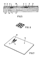
La figure 5 représente en coupe une carte portative obtenue par le procédé selon l'invention.FIG. 5 represents in section a portable card obtained by the method according to the invention.
Les figures 6 et 7 représentent en perspective des exemples de dispositifs obtenus par le procédé selon l'invention.Figures 6 and 7 show in perspective examples of devices obtained by the method according to the invention.
La figure 1 représente une pastille de circuit à semiconducteur 5, munie de métallisations 3, et un support mince 2 muni de pistes conductrices métalliques 1 portées par une première face 8 de ce support mince. Dans ce support, sont réalisés des trous 4 avec une configuration correspondant à celle des métallisations 3 sur la pastille.FIG. 1 represents a
Les trous dans le support sont disposés de telle façon qu'en appliquant la pastille contre le support avec un positionnement adéquat, on ait un trou du support en face de chaque métallisation de la pastille.The holes in the support are arranged in such a way that by applying the tablet against the support with an adequate positioning, there is a hole in the support opposite each metallization of the tablet.
Les pistes conductrices 1 sont disposées de façon à comporter des portions en bordure des trous. De preférence, ces portions en bordure des trous sont constituées par des anneaux entourant les trous, appelés habituellement lunules. Le support et les pistes sont constitués par un classique circuit imprimé mince, dit "simple face", sur lequel on monte un grand nombre de pastilles, et que l'on découpe en petits morceaux contenant chacun soit une pastille, soit plusieurs pastilles interconnectées.The
Le support peut également être constitué par un film en forme de ruban éventuellement muni de trous de positionnement et portant des pistes métalliques déposées sur une de ses faces. Ce film, muni de pastilles par le procédé de l'invention, et enroulé sur une bobine, est utilisé dans une machine qui le découpe et reporte sur des circuits électroniques des portions de film munies chacune d'une pastille.The support can also be constituted by a film in the form of a ribbon possibly provided with positioning holes and carrying metal tracks deposited on one of its faces. This film, provided with pellets by the method of the invention, and wound on a reel, is used in a machine which cuts it and transfers onto electronic circuits portions of film each provided with a tablet.
Afin d'assurer une mise en oeuvre efficace du procédé selon l'invention, il importe que certaines proportions dimensionnelles soient respectées. En particulier, il convient que l'épaisseur H du support soit relativement faible devant la dimension des trous, celle-ci étant du même ordre de grandeur que celle des métallisations: on emploie de préférence une épaisseur H inférieure à 0,3 mm.In order to ensure an efficient implementation of the method according to the invention, it is important that certain dimensional proportions are respected. In particular, the thickness H of the support should be relatively small compared to the dimension of the holes, the latter being of the same order of magnitude as that of the metallizations: a thickness H of less than 0.3 mm is preferably used.
En utilisant une technologie classique de circuit imprimé pour réaliser le support 2, par exemple en verre époxy, on est capable, d'une façon courante, de réaliser des trous ronds de diamètre B = 0,4 mm. L'épaisseur H étant égale, par exemple à 0,1 mm, on a ainsi un trou quatre fois plus large que sa profondeur.By using a conventional printed circuit technology to produce the support 2, for example in epoxy glass, it is possible, in a current manner, to produce round holes of diameter B = 0.4 mm. The thickness H being equal, for example to 0.1 mm, there is thus a hole four times wider than its depth.
Les métallisations 3 de la pastille sont un peu plus grandes. Par exemple, elles peuvent avoir une largeur A de 0,5 mm. Ceci est une dimension notablement plus grande qu'il est d'usage en matière de circuits intégrés. Il faut bien voir que l'invention s'applique de préférence à des circuits intégrés présentant une grande complexité, mais comportant malgré cela un nombre réduit de métallisations d'entrée/sortie. C'est le cas, par exemple, des circuits utilisés pour les cartes de paiement, qui offrent des fonctions logiques multiples et complexes et ne comportent que huit ou même seulement six bornes. Supposons par exemple qu'une pastille portant un tel circuit ait une surface de 15 mm2 avec six métallisations de 0,1 mm x 0,1 mm. Si on porte à 0,5 x 0,5 mm la dimension de ses métallisations, on accroît de 1,44 mm2 la surface, soit à peine 10 % de la surface totale de la pastille. On accroît d'à peu près autant le prix d'une pastille, mais le gain réalisé grâce à la simplification du montage est supérieur à l'augmentation de prix de la pastille, et finalement le produit revient moins cher.The
Il est possible également de réaliser des trous plus petits, grâce à l'emploi d'un laser. Pour garder cependant une tolérance de positionnement raisonnable, ainsi qu'un rapport B/H suffisant, il est toujours avantageux, là encore, d'utiliser des métallisations un peu plus grandes qu'il estd'usage. On pourra par exemple réaliser des trous B = 0,2 mm et utiliser des métallisations avec A = 0,3 mm, l'épaisseur H étant toujours de 0,1 mm. Dans l'exemple cidessus, cela correspondrait à une augmentation de surface de la pastille de seulement 3,2 %.It is also possible to make smaller holes, thanks to the use of a laser. To keep a reasonable positioning tolerance, as well as a sufficient B / H ratio, it is still advantageous, here again, to use metallizations a little larger than it is used. We could for example make holes B = 0.2 mm and use metallizations with A = 0.3 mm, the thickness H always being 0.1 mm. In the example above, this would correspond to an increase in surface area of the tablet of only 3.2%.
A partir d'un tel support et d'une telle pastille, et la seconde face 7 du support mince, opposée à celle 8 qui porte les métallisations, étant entièrement isolante, on place la pastille 5 sur cette seconde face 7 avec ses métallisations 3 tournées vers cette seconde face et en correspondance avec les trous 4 et, ainsi que le représente la figure 2, on dépose à partir de la première face 8 un îlot de pâte conductrice polymérisable 6 sur chaque trou de façon à recouvrir à la fois la métallisation placée sous le trou et la piste conductrice 1 en bordure dudit trou.From such a support and such a patch, and the second face 7 of the thin support, opposite to that 8 which carries the metallizations, being entirely insulating, the
Cette pâte est alors amenée de préférence en utilisant un écran ou un pochoir et une raclette. L'écran est par exemple constitué d'un tissu recouvert d'un enduit photogravé dans le procédé bien connu dit: de sérigraphie. Dans ce cas, la pastille et le support sont maintenus en place pendant le dépôt de la pàte par un moyen mécanique connu, par exemple une plaque munie de trous et une aspiration, à la suite de quoi la viscosité et l'adhérence de la pàte sont suffisantes pour maintenir la pastille pendant les manipulations subséquentes jusqu'à ce qu'on ait assuré la polymérisation de la pàte, par exemple par chauffage dans un four.This paste is then preferably brought in using a screen or a stencil and a squeegee. The screen is for example made of a fabric covered with a coating photo-etched in the well-known process known as: screen printing. In this case, the tablet and the support are held in place during the deposition of the dough by known mechanical means, for example a plate provided with holes and a suction, as a result of which the viscosity and the adhesion of the dough are sufficient to maintain the pellet during subsequent manipulations until the polymerization of the dough has been ensured, for example by heating in an oven.
Dans ce cas, les métallisations de la pastille sont de préférence constituées d'un empilage titane/platine/or qui donne de bons résultats avec la plupart des pâtes conductrices du commerce.In this case, the metallizations of the tablet preferably consist of a titanium / platinum / gold stack which gives good results with most commercially available conductive pastes.
La pastille peut aussi être maintenue grâce à une cale 17, d'épaisseur égale à, ou légèrement plus faible que celle de la pastille 5.The pellet can also be maintained thanks to a
Une paroi non représentée est fixée à la face intérieure du dispositif et maintient la pastille en place, au moins pendant le dépôt et, éventuellement, la polymérisation de la matière conductrice 6. Cette paroi peut, par exemple, être faite d'un ruban adhésif.A wall (not shown) is fixed to the interior face of the device and keeps the tablet in place, at least during the deposition and, if necessary, the polymerization of the conductive material 6. This wall can, for example, be made of adhesive tape .
La pastille peut également être maintenue par un cordon de matière adéquate déposée le long du périmètre de la pastille, entre cette dernière et la cale 17. Une telle matière peut être une pâte isolante polymérisable ou un verre fusible à basse température. Cette disposition a l'avantage de procurer ultérieurement une protection climatique de la pastille.The pellet can also be held by a bead of suitable material deposited along the perimeter of the pellet, between the latter and the
La cale 17 peut être collée sur le support 2, par exemple selon un procédé connu de pressage des circuits imprimés multicouches.The
Au lieu d'un support mince plat 2 et d'une cale 17, on peut aussi utiliser, ainsi que le réprésente la figure 4, un support d'un seul tenant 2 dans lequel on creuse un évidement pour loger la pastille 5. Cet évidement ne débouche pas et laisse une paroi 20 constituant le support mince proprement dit. Ce support est meilleur marché que celui de la figure 2 car il n'utilise qu'une seule feuille et on évite un pressage.Instead of a thin flat support 2 and a
Ce support peut aussi être réalisé en céramique, ce qui présente plusieurs avantages: l'évidement peut alors être obtenu, de même que les trous, directement par moulage, et on peut utiliser, pour assurer la meilleure étanchéité possible le long du périmétre de la pastille, un verre fusible à une température pouvant atteindre 300 à 400° C. les divers coefficients de dilatation (silicium, verre, céramique) étant bien accordés.This support can also be made of ceramic, which has several advantages: the recess can then be obtained, as well as the holes, directly by molding, and it can be used, to ensure the best possible seal along the perimeter of the pellet, a glass fusible at a temperature up to 300 to 400 ° C. the various expansion coefficients (silicon, glass, ceramic) being well tuned.
En perfectionnant encore l'idée de l'invention, on utilise un support entièrement isolant, tel que représenté en 2 sur la figure 4, on place la pastille 5 sur une face 7 de ce support, avec ses métallisations 3 tournées vers cette face et en correspondance avec les trous 4, et on constitue alors les pistes 9 sur l'autre face au moyen d'une pâte conductrice, en leur donnant une configuration telle que des portions de pistes recouvrent les trous 4 afin que la pâte y pénètre, venant ainsi en contact avec les métallisations 3 de la pastille. Ces pistes 9 sont de préférence déposées au moyen d'une sérigraphie.By further refining the idea of the invention, a fully insulating support is used, as shown in 2 in FIG. 4, the
Bien entendu c'est tout à fait par hasard que l'on a représenté la piste 9 sur un support d'une seule pièce 2, alors que sur la figure 2 on a représenté une piste préexistante 1 sur un support 2, 7 constitué de deux feuilles superposées. Il va de soi que chacun des deux types de support peut être utilisé indifféremment avec chacun des types de pistes conductrices.Of course, it is entirely by chance that the
La figure 3 représente des portions de pastille 5 avec des métallisations 3. Sur chaque métallisation on a soudé, avant la découpe des tranches de matériau semiconducteur fournissant les pastilles, une portion de fil métallique. A gauche de la figure, un fil 12 a été soudé en deux points voisins sur la même métallisation en formant ainsi une sorte d'anse de panier qui améliore l'accrochage du matériau conducteur à la métallisation. Il faut bien voir cependant, que ces dispositions seulement destinées à obtenir un meilleur rendement et une meilleure fiabilité, ne sont pas indispensable pour la mise en oeuvre de l'invention.FIG. 3 represents portions of
Dans le cas ou le produit à réaliser est une carte électronique portative, ainsi qu'il a été indiqué en préambule, on peut avantageusement, au lieu d'inclure un support dans la carte, réaliser celle ci de telle façon qu'elle constitue elle même directement le support de la pastille de circuit intégré.In the case where the product to be produced is a portable electronic card, as indicated in the preamble, it is advantageously possible, instead of including a support in the card, to produce the latter in such a way that it constitutes it even directly the support of the integrated circuit chip.
Une telle carte offre des éléments conducteurs plats (10, figure 7) qui servent à établir des contacts électriques avec un appareil au moyen duquel la carte est exploitée. Ces éléments conducteurs plats peuvent être réalisés au moyen d'une pâte conductrice, et doivent être réunis aux bornes du circuit à semiconducteur inclus directement dans la carte.Such a card offers flat conductive elements (10, FIG. 7) which serve to establish electrical contacts with a device by means of which the card is operated. These flat conductive elements can be produced by means of a conductive paste, and must be joined at the terminals of the semiconductor circuit included directly in the card.
La figure 5 représente des feuilles empilées 21, 22, 23,24. Les feuilles centrales 22, 23 ont une épaisseur sensiblement égale à celle de la pastille 5. Les deux couches externes 21 et 24 permettent d'enfermer la pastille 5 dans l'ensemble. Une fois cet empilage pressé à chaud avec la pastille 5 à l'intérieur, celle ci se trouve placée très près d'une face de la carte, ici la face supérieure, avec ses métallisations 3 tournées vers ladite face. On a donc constitué une paroi mince 20 en face de la pastille. On a ménagé des trous 4 dans cette paroi mince, préalablement au pressage de l'empilage, et placé la feuille 21 de telle façon que ces trous soient en regard des métallisations 3 de la pastille. Les feuilles 21 à 24 constituant la carte peuvent être en chlorure de polyvinyle dit PVC, et pressées selon la technique habituelle de fabrication des cartes portatives à pistes magnétiques. Elles peuvent aussi être en laminé de fibre de verre et époxy, telles qu'on en utilise pour réaliser les circuits imprimés multicouches, et pressées selon la technique connue de ces circuits. On peut aussi réaliser l'ensemble correspondant aux feuilles 21, 22, 23 d'un seul tenant, par exemple en le moulant avec une des nombreuses matières susceptibles d'être moulées par transfert. Les trous 4 viendront alors de moulage. La pastille 5 sera alors mise en place, par exemple collée sur la feuille 24, et celle ci à son tour collée sur l'ensemble 21, 22, 23.FIG. 5 represents stacked
Une fois constitué l'ensemble avec la pastille à l'intérieur, on constitue les susdits éléments conducteurs plats par sérigraphie d'une pâte conductrice à basse température de polymérisation, et en même temps que l'on constitue ces éléments, on fait s'étendre la pâte conductrice depuis chaque éléments jusqu'à la métallisation afférente de la pastille, en la faisant pénétrer dans les trous: ainsi le dessin des conducteurs formés au moyen de sérigraphie est tel qu'un motif unique constitue un susdit élément conducteur plat et une piste conductrice le reliant à la pastille de circuit intégré, et que chaque piste recouvre un trou de façon que sa matière y pénètre et fasse contact avec une métallisation de la pastille.Once the assembly has been made with the pellet inside, the above-mentioned flat conductive elements are formed by screen printing of a conductive paste at low polymerization temperature, and at the same time as these elements are formed, extend the conductive paste from each element to the associated metallization of the pellet, making it penetrate into the holes: thus the design of the conductors formed by screen printing is such that a single pattern constitutes a above-mentioned flat conductive element and a conductive track connecting it to the integrated circuit chip, and each track covers a hole so that its material penetrates there and makes contact with a metallization of the chip.
Une feuille protectrice 11 peut enfin être collée sur l'empilage pour protéger les pistes 9 et les éléments conducteurs plats. Bien entendu, des orifices sont prévus dans cette feuille 11 pour donner accès aux conducteurs plats.A
La figure 6 représente un support de circuit intégré réalisé selon le procédé de l'invention et destiné à être utilisé dans un sous-ensemble électronique, ou aussi à être inclus dans une carte portative.FIG. 6 represents an integrated circuit support produced according to the method of the invention and intended to be used in an electronic sub-assembly, or also to be included in a portable card.
La figure 7 qui représente une carte portative constituant directement le support d'une pastille de circuit intégré permet de bien se rendre compte de la configuration des conducteurs. Les susdits éléments conducteurs plats sont représentés en 10, les pistes en 9. Celles-ci se terminent par des plots arrondis au-dessus de chaque trou pour prendre contact avec la pastille "enterrée" dont la position est indiquée par la flèche 5.FIG. 7 which represents a portable card directly constituting the support of an integrated circuit chip makes it possible to appreciate the configuration of the conductors. The above flat conductive elements are represented at 10, the tracks at 9. These end in rounded studs above each hole to make contact with the "buried" patch, the position of which is indicated by
Il va de soi que le procédé selon l'invention gagne à être utilisé dans un processus de fabrication dit "en multiple", c'est-à-dire qu'on fabrique une plaque ou une bande contenant un grand nombre de dispositifs tels que ceux des figures 6 ou 7, et qu'on découpe tout à fait à la fin les plaques ou les bandes pour obtenir des dispositifs individuels.It goes without saying that the method according to the invention deserves to be used in a so-called "multiple" manufacturing process, that is to say that a plate or a strip is produced containing a large number of devices such as those of FIGS. 6 or 7, and that the plates or the strips are entirely cut at the end in order to obtain individual devices.
Claims (4)
Applications Claiming Priority (2)
| Application Number | Priority Date | Filing Date | Title |
|---|---|---|---|
| FR8208430A FR2527036A1 (en) | 1982-05-14 | 1982-05-14 | METHOD FOR CONNECTING A SEMICONDUCTOR TO ELEMENTS OF A SUPPORT, PARTICULARLY A PORTABLE CARD |
| FR8208430 | 1982-05-14 |
Publications (2)
| Publication Number | Publication Date |
|---|---|
| EP0094716A1 EP0094716A1 (en) | 1983-11-23 |
| EP0094716B1 true EP0094716B1 (en) | 1987-01-14 |
Family
ID=9274042
Family Applications (1)
| Application Number | Title | Priority Date | Filing Date |
|---|---|---|---|
| EP83200661A Expired EP0094716B1 (en) | 1982-05-14 | 1983-05-06 | Process for connecting a semiconductor to elements of a support, particularly of a portable card |
Country Status (6)
| Country | Link |
|---|---|
| US (1) | US4731645A (en) |
| EP (1) | EP0094716B1 (en) |
| JP (1) | JPS58209133A (en) |
| CA (1) | CA1201821A (en) |
| DE (1) | DE3369233D1 (en) |
| FR (1) | FR2527036A1 (en) |
Cited By (1)
| Publication number | Priority date | Publication date | Assignee | Title |
|---|---|---|---|---|
| DE3805130A1 (en) * | 1987-02-20 | 1988-09-01 | Mitsubishi Electric Corp | HOUSING FOR A SEMICONDUCTOR ARRANGEMENT |
Families Citing this family (62)
| Publication number | Priority date | Publication date | Assignee | Title |
|---|---|---|---|---|
| FR2555744B1 (en) * | 1983-11-30 | 1986-05-09 | Philips Ind Commerciale | SPECIMEN WITH MEANS FOR STORING ANALYSIS RESULTS |
| EP0147099B1 (en) * | 1983-12-06 | 1992-06-17 | Mars Incorporated | Tokens and token handling devices |
| JPH0815187B2 (en) * | 1984-02-17 | 1996-02-14 | 株式会社東芝 | Method of manufacturing integrated circuit device |
| JPS6146736U (en) * | 1984-08-31 | 1986-03-28 | カシオ計算機株式会社 | Semiconductor chip mounting structure |
| CH661808A5 (en) * | 1985-01-21 | 1987-08-14 | Lupa Finances | CARD PROVIDED WITH A MICROPROCESSOR AND / OR AT LEAST ONE ELECTRONIC MEMORY. |
| JPH0751390B2 (en) * | 1985-07-10 | 1995-06-05 | カシオ計算機株式会社 | IC card |
| US4889980A (en) * | 1985-07-10 | 1989-12-26 | Casio Computer Co., Ltd. | Electronic memory card and method of manufacturing same |
| JPH074995B2 (en) * | 1986-05-20 | 1995-01-25 | 株式会社東芝 | IC card and method of manufacturing the same |
| DE3639630A1 (en) * | 1986-11-20 | 1988-06-01 | Gao Ges Automation Org | DATA CARRIER WITH INTEGRATED CIRCUIT AND METHOD FOR PRODUCING THE SAME |
| JPS63149191A (en) * | 1986-12-15 | 1988-06-21 | 日立マクセル株式会社 | Ic card |
| JP2579937B2 (en) * | 1987-04-15 | 1997-02-12 | 株式会社東芝 | Electronic circuit device and method of manufacturing the same |
| FR2635916B1 (en) * | 1988-08-23 | 1990-10-12 | Bull Sa | HIGH DENSITY INTEGRATED CIRCUIT SUPPORT AND MANUFACTURING METHOD THEREOF |
| US6938825B1 (en) | 1989-04-24 | 2005-09-06 | Ultracard, Inc. | Data system |
| US5107099A (en) * | 1989-04-24 | 1992-04-21 | Smith Malcolm G | Magnetic card reader and method |
| US5157244A (en) * | 1989-12-19 | 1992-10-20 | Amp Incorporated | Smart key system |
| JPH0463282U (en) * | 1990-10-04 | 1992-05-29 | ||
| EP0569417B1 (en) * | 1991-01-28 | 1995-07-05 | Siemens Aktiengesellschaft | Process for making a portable data support |
| JP2816028B2 (en) * | 1991-02-18 | 1998-10-27 | 株式会社東芝 | Method for manufacturing semiconductor device |
| US5422514A (en) * | 1993-05-11 | 1995-06-06 | Micromodule Systems, Inc. | Packaging and interconnect system for integrated circuits |
| DE4325458A1 (en) * | 1993-07-29 | 1995-02-09 | Orga Bond Technik Gmbh | Support element for an IC module |
| FR2721732B1 (en) * | 1994-06-22 | 1996-08-30 | Solaic Sa | Contactless memory card whose electronic circuit includes a module. |
| DE19539181C2 (en) * | 1995-10-20 | 1998-05-14 | Ods Gmbh & Co Kg | Chip card module and corresponding manufacturing process |
| US6013948A (en) | 1995-11-27 | 2000-01-11 | Micron Technology, Inc. | Stackable chip scale semiconductor package with mating contacts on opposed surfaces |
| US5674785A (en) * | 1995-11-27 | 1997-10-07 | Micron Technology, Inc. | Method of producing a single piece package for semiconductor die |
| US6861290B1 (en) * | 1995-12-19 | 2005-03-01 | Micron Technology, Inc. | Flip-chip adaptor package for bare die |
| US5811879A (en) * | 1996-06-26 | 1998-09-22 | Micron Technology, Inc. | Stacked leads-over-chip multi-chip module |
| JP2777114B2 (en) * | 1996-09-02 | 1998-07-16 | 株式会社日立製作所 | Tape carrier |
| US6250192B1 (en) * | 1996-11-12 | 2001-06-26 | Micron Technology, Inc. | Method for sawing wafers employing multiple indexing techniques for multiple die dimensions |
| DE19735171A1 (en) * | 1997-08-13 | 1999-01-07 | Siemens Ag | Semiconductor module useful for chip card |
| US5899705A (en) | 1997-11-20 | 1999-05-04 | Akram; Salman | Stacked leads-over chip multi-chip module |
| DE19809073A1 (en) * | 1998-03-04 | 1999-09-16 | Orga Kartensysteme Gmbh | Semiconductor chip module for chip card |
| US6208019B1 (en) * | 1998-03-13 | 2001-03-27 | Kabushiki Kaisha Toshiba | Ultra-thin card-type semiconductor device having an embredded semiconductor element in a space provided therein |
| USRE43112E1 (en) | 1998-05-04 | 2012-01-17 | Round Rock Research, Llc | Stackable ball grid array package |
| US6414391B1 (en) * | 1998-06-30 | 2002-07-02 | Micron Technology, Inc. | Module assembly for stacked BGA packages with a common bus bar in the assembly |
| DE19830540A1 (en) * | 1998-07-08 | 2000-01-13 | Siemens Ag | Electronic flexible type circuit board especially for power semiconductors, sensors and passive components |
| US6871787B1 (en) | 1998-07-10 | 2005-03-29 | Ultracard, Inc. | Data storage card having a glass substrate and data surface region and method for using same |
| JP2000099678A (en) * | 1998-09-18 | 2000-04-07 | Hitachi Ltd | Ic card and its production |
| DE19845665C2 (en) * | 1998-10-05 | 2000-08-17 | Orga Kartensysteme Gmbh | Method for producing a carrier element for an IC chip for installation in chip cards |
| US6815251B1 (en) | 1999-02-01 | 2004-11-09 | Micron Technology, Inc. | High density modularity for IC's |
| DE19940480C2 (en) * | 1999-08-26 | 2001-06-13 | Orga Kartensysteme Gmbh | Conductor carrier layer for lamination into a chip card, chip card with a conductor carrier carrier layer and method for producing a chip card |
| US7036739B1 (en) | 1999-10-23 | 2006-05-02 | Ultracard, Inc. | Data storage device apparatus and method for using same |
| US7487908B1 (en) | 1999-10-23 | 2009-02-10 | Ultracard, Inc. | Article having an embedded accessible storage member, apparatus and method for using same |
| US8397998B1 (en) | 1999-10-23 | 2013-03-19 | Ultracard, Inc. | Data storage device, apparatus and method for using same |
| DE19955538B4 (en) * | 1999-11-18 | 2014-06-05 | Morpho Cards Gmbh | Printed conductor carrier layer for lamination into a chip card, method for producing a conductor carrier layer Injection molding tool for carrying out the method for producing a conductor carrier layer |
| DE10014379A1 (en) | 2000-03-23 | 2001-10-11 | Infineon Technologies Ag | Method and device for connecting at least one chip to a rewiring arrangement |
| DE10042312A1 (en) * | 2000-08-29 | 2002-03-14 | Orga Kartensysteme Gmbh | Method for producing a carrier element for an IC chip |
| US6969006B1 (en) | 2000-09-15 | 2005-11-29 | Ultracard, Inc. | Rotable portable card having a data storage device, apparatus and method for using same |
| US6707149B2 (en) * | 2000-09-29 | 2004-03-16 | Tessera, Inc. | Low cost and compliant microelectronic packages for high i/o and fine pitch |
| FR2816107B1 (en) * | 2000-10-30 | 2003-11-28 | Gemplus Card Int | MOVIE INTEGRATED CIRCUIT MODULE AND MANUFACTURING METHOD THEREOF |
| FR2818802B1 (en) * | 2000-12-21 | 2003-11-28 | Gemplus Card Int | CONNECTION BY CUT-OUT INSULATOR AND PRINTED CORD IN PLAN |
| FR2822338B1 (en) * | 2001-03-14 | 2003-06-27 | Sagem | METHOD FOR ELECTRICALLY CONNECTING CONTACT PLOTS OF A MICROELECTRONIC COMPONENT DIRECTLY TO PRINTED CIRCUIT TRACKS, AND PRINTED CIRCUIT PLATE THUS MADE UP |
| JP3678212B2 (en) * | 2002-05-20 | 2005-08-03 | ウシオ電機株式会社 | Super high pressure mercury lamp |
| US6755700B2 (en) * | 2002-11-12 | 2004-06-29 | Modevation Enterprises Inc. | Reset speed control for watercraft |
| US20040102753A1 (en) * | 2002-11-26 | 2004-05-27 | Kimberly-Clark Worldwide, Inc. | Male incontinence absorbent article and method of producing same |
| FI20031341A (en) | 2003-09-18 | 2005-03-19 | Imbera Electronics Oy | Method for manufacturing an electronic module |
| FI117814B (en) * | 2004-06-15 | 2007-02-28 | Imbera Electronics Oy | A method for manufacturing an electronic module |
| JP2008544512A (en) * | 2005-06-16 | 2008-12-04 | イムベラ エレクトロニクス オサケユキチュア | Circuit board structure and manufacturing method thereof |
| FI119714B (en) | 2005-06-16 | 2009-02-13 | Imbera Electronics Oy | Circuit board structure and method for manufacturing a circuit board structure |
| FI122128B (en) * | 2005-06-16 | 2011-08-31 | Imbera Electronics Oy | Process for manufacturing circuit board design |
| US10206288B2 (en) * | 2015-08-13 | 2019-02-12 | Palo Alto Research Center Incorporated | Bare die integration with printed components on flexible substrate |
| US10165677B2 (en) | 2015-12-10 | 2018-12-25 | Palo Alto Research Center Incorporated | Bare die integration with printed components on flexible substrate without laser cut |
| US10847384B2 (en) | 2017-05-31 | 2020-11-24 | Palo Alto Research Center Incorporated | Method and fixture for chip attachment to physical objects |
Family Cites Families (12)
| Publication number | Priority date | Publication date | Assignee | Title |
|---|---|---|---|---|
| DE2202348A1 (en) * | 1972-01-19 | 1973-07-26 | Siemens Ag | CROSS BAR DISTRIBUTOR |
| JPS5180770A (en) * | 1975-01-13 | 1976-07-14 | Suwa Seikosha Kk | |
| GB1565207A (en) * | 1975-09-05 | 1980-04-16 | Sinclair Radionics | Printed circuits |
| US4222516A (en) * | 1975-12-31 | 1980-09-16 | Compagnie Internationale Pour L'informatique Cii-Honeywell Bull | Standardized information card |
| FR2382101A1 (en) * | 1977-02-28 | 1978-09-22 | Labo Electronique Physique | Metallised perforated polyimide film strip convectors - for semiconductor circuits for close coupled terminals without localised metallisation |
| US4246595A (en) * | 1977-03-08 | 1981-01-20 | Matsushita Electric Industrial Co., Ltd. | Electronics circuit device and method of making the same |
| DE2920012B1 (en) * | 1979-05-17 | 1980-11-20 | Gao Ges Automation Org | ID card with IC module and method for producing such an ID card |
| JPS5649178U (en) * | 1979-09-21 | 1981-05-01 | ||
| US4544989A (en) * | 1980-06-30 | 1985-10-01 | Sharp Kabushiki Kaisha | Thin assembly for wiring substrate |
| FR2490059A1 (en) * | 1980-09-09 | 1982-03-12 | Serras Paulet Edouard | PRINTED CIRCUIT AND MANUFACTURING METHOD THEREOF |
| US4549247A (en) * | 1980-11-21 | 1985-10-22 | Gao Gesellschaft Fur Automation Und Organisation Mbh | Carrier element for IC-modules |
| DE3153768C2 (en) * | 1981-04-14 | 1995-11-09 | Gao Ges Automation Org | Plastics identity card with an internal integrated circuit |
-
1982
- 1982-05-14 FR FR8208430A patent/FR2527036A1/en active Granted
-
1983
- 1983-05-06 EP EP83200661A patent/EP0094716B1/en not_active Expired
- 1983-05-06 DE DE8383200661T patent/DE3369233D1/en not_active Expired
- 1983-05-12 CA CA000428006A patent/CA1201821A/en not_active Expired
- 1983-05-14 JP JP58083521A patent/JPS58209133A/en active Pending
-
1986
- 1986-06-12 US US06/873,875 patent/US4731645A/en not_active Expired - Fee Related
Cited By (1)
| Publication number | Priority date | Publication date | Assignee | Title |
|---|---|---|---|---|
| DE3805130A1 (en) * | 1987-02-20 | 1988-09-01 | Mitsubishi Electric Corp | HOUSING FOR A SEMICONDUCTOR ARRANGEMENT |
Also Published As
| Publication number | Publication date |
|---|---|
| US4731645A (en) | 1988-03-15 |
| FR2527036A1 (en) | 1983-11-18 |
| DE3369233D1 (en) | 1987-02-19 |
| JPS58209133A (en) | 1983-12-06 |
| CA1201821A (en) | 1986-03-11 |
| FR2527036B1 (en) | 1985-02-01 |
| EP0094716A1 (en) | 1983-11-23 |
Similar Documents
| Publication | Publication Date | Title |
|---|---|---|
| EP0094716B1 (en) | Process for connecting a semiconductor to elements of a support, particularly of a portable card | |
| EP0638933B1 (en) | Interconnection process of stacked semi-conductors chips and devices | |
| EP0296511B1 (en) | Method of fabricating a tape intended to provide circuits for electronic modules, and tape obtained by this method | |
| EP0307773B1 (en) | Method of manufacturing electronic modules, especially for smart cards | |
| EP0207853B1 (en) | Method for mounting an integrated circuit on a support, resultant device and its use in an electronic microcircuit card | |
| EP0128822B1 (en) | Method of producing memory cards, and cards obtained thereby | |
| FR2614492A1 (en) | CIRCUIT PROVIDED WITH TERMINAL ELEMENTS AND MANUFACTURING METHOD THEREOF | |
| FR2736740A1 (en) | PROCESS FOR PRODUCING AND ASSEMBLING INTEGRATED CIRCUIT BOARD AND CARD THUS OBTAINED | |
| EP0593330B1 (en) | 3D-interconnection method for electronic component housings and resulting 3D component | |
| EP0044247B1 (en) | Method of producing a carrier for electronic components for the interconnection of integrated-circuit chips | |
| EP0321327B1 (en) | Method of mounting an electronic component and its electronic connections on a support | |
| EP3020256B1 (en) | Electronic module with adhesive dielectric film and method for manufacturing same | |
| FR2635920A1 (en) | METHOD FOR MANUFACTURING A CONNECTION ZONE FOR A TRIPLATE-TYPE MICROWAVE CIRCUIT AND CIRCUIT THUS OBTAINED | |
| FR2963849A1 (en) | METHOD OF MANUFACTURING AN ELECTRIC CIRCUIT AND CIRCUIT OBTAINED | |
| EP0313456B1 (en) | Copolymers useful as multifunctional additives in lubricants, and compositions containing these copolymers | |
| EP0305267B1 (en) | Production method of the totality of conducting patterns on an insulating surface of complex shape | |
| WO1998057298A1 (en) | Method for making a contactless smart card | |
| EP1192592A1 (en) | Device and method for making devices comprising at least a chip fixed on a support | |
| EP1623367A1 (en) | Method for making a pre-laminated inlet | |
| FR2694139A1 (en) | Interconnection substrate for electronic components e.g. leadless chip carrier mounted integrated circuits - has double layer composite material core with printed circuit formed on each substrate exterior surface, with cores connected by electrically isolating fibres and has metallised through holes insulated from cores | |
| EP0163581B1 (en) | Production method and device for electrical connections between two printed-circuit boards, and electrical connection method using the device | |
| EP1210690B1 (en) | Electronic device comprising a chip fixed on a support and method for making same | |
| WO2005064533A1 (en) | Methods for the production of an external-contact-free card and card thus obtained | |
| FR2739742A1 (en) | METHOD FOR MANUFACTURING MICRO-COMPONENT MODULE AND SUPPORT FOR PRINTED BOND CIRCUITS, AND INTERMEDIATE PRODUCT FOR IMPLEMENTING THE METHOD | |
| EP0168287A1 (en) | Process for making printed circuits, and printed circuit obtained by this method |
Legal Events
| Date | Code | Title | Description |
|---|---|---|---|
| PUAI | Public reference made under article 153(3) epc to a published international application that has entered the european phase |
Free format text: ORIGINAL CODE: 0009012 |
|
| AK | Designated contracting states |
Designated state(s): CH DE FR GB IT LI SE |
|
| 17P | Request for examination filed |
Effective date: 19840105 |
|
| RAP1 | Party data changed (applicant data changed or rights of an application transferred) |
Owner name: N.V. PHILIPS' GLOEILAMPENFABRIEKEN Owner name: RTC-COMPELEC |
|
| GRAA | (expected) grant |
Free format text: ORIGINAL CODE: 0009210 |
|
| AK | Designated contracting states |
Kind code of ref document: B1 Designated state(s): CH DE FR GB IT LI SE |
|
| REF | Corresponds to: |
Ref document number: 3369233 Country of ref document: DE Date of ref document: 19870219 |
|
| ITF | It: translation for a ep patent filed |
Owner name: ING. C. GREGORJ S.P.A. |
|
| PLBE | No opposition filed within time limit |
Free format text: ORIGINAL CODE: 0009261 |
|
| STAA | Information on the status of an ep patent application or granted ep patent |
Free format text: STATUS: NO OPPOSITION FILED WITHIN TIME LIMIT |
|
| 26N | No opposition filed | ||
| PGFP | Annual fee paid to national office [announced via postgrant information from national office to epo] |
Ref country code: GB Payment date: 19900430 Year of fee payment: 8 |
|
| REG | Reference to a national code |
Ref country code: FR Ref legal event code: CA |
|
| PGFP | Annual fee paid to national office [announced via postgrant information from national office to epo] |
Ref country code: SE Payment date: 19900522 Year of fee payment: 8 Ref country code: FR Payment date: 19900522 Year of fee payment: 8 |
|
| ITTA | It: last paid annual fee | ||
| PGFP | Annual fee paid to national office [announced via postgrant information from national office to epo] |
Ref country code: DE Payment date: 19900725 Year of fee payment: 8 |
|
| PGFP | Annual fee paid to national office [announced via postgrant information from national office to epo] |
Ref country code: CH Payment date: 19900824 Year of fee payment: 8 |
|
| REG | Reference to a national code |
Ref country code: FR Ref legal event code: CD |
|
| PG25 | Lapsed in a contracting state [announced via postgrant information from national office to epo] |
Ref country code: GB Effective date: 19910506 |
|
| PG25 | Lapsed in a contracting state [announced via postgrant information from national office to epo] |
Ref country code: SE Effective date: 19910507 |
|
| PG25 | Lapsed in a contracting state [announced via postgrant information from national office to epo] |
Ref country code: LI Effective date: 19910531 Ref country code: CH Effective date: 19910531 |
|
| GBPC | Gb: european patent ceased through non-payment of renewal fee | ||
| PG25 | Lapsed in a contracting state [announced via postgrant information from national office to epo] |
Ref country code: FR Effective date: 19920131 |
|
| REG | Reference to a national code |
Ref country code: CH Ref legal event code: PL |
|
| PG25 | Lapsed in a contracting state [announced via postgrant information from national office to epo] |
Ref country code: DE Effective date: 19920303 |
|
| REG | Reference to a national code |
Ref country code: FR Ref legal event code: ST |
|
| EUG | Se: european patent has lapsed |
Ref document number: 83200661.3 Effective date: 19911209 |