EP0093202A1 - Poly-(halostyrène) pour compositions de réserve négatives - Google Patents
Poly-(halostyrène) pour compositions de réserve négatives Download PDFInfo
- Publication number
- EP0093202A1 EP0093202A1 EP82111811A EP82111811A EP0093202A1 EP 0093202 A1 EP0093202 A1 EP 0093202A1 EP 82111811 A EP82111811 A EP 82111811A EP 82111811 A EP82111811 A EP 82111811A EP 0093202 A1 EP0093202 A1 EP 0093202A1
- Authority
- EP
- European Patent Office
- Prior art keywords
- halostyrene
- poly
- range
- solvent
- monomer
- Prior art date
- Legal status (The legal status is an assumption and is not a legal conclusion. Google has not performed a legal analysis and makes no representation as to the accuracy of the status listed.)
- Granted
Links
Images


Classifications
-
- G—PHYSICS
- G03—PHOTOGRAPHY; CINEMATOGRAPHY; ANALOGOUS TECHNIQUES USING WAVES OTHER THAN OPTICAL WAVES; ELECTROGRAPHY; HOLOGRAPHY
- G03F—PHOTOMECHANICAL PRODUCTION OF TEXTURED OR PATTERNED SURFACES, e.g. FOR PRINTING, FOR PROCESSING OF SEMICONDUCTOR DEVICES; MATERIALS THEREFOR; ORIGINALS THEREFOR; APPARATUS SPECIALLY ADAPTED THEREFOR
- G03F7/00—Photomechanical, e.g. photolithographic, production of textured or patterned surfaces, e.g. printing surfaces; Materials therefor, e.g. comprising photoresists; Apparatus specially adapted therefor
- G03F7/004—Photosensitive materials
- G03F7/038—Macromolecular compounds which are rendered insoluble or differentially wettable
-
- C—CHEMISTRY; METALLURGY
- C08—ORGANIC MACROMOLECULAR COMPOUNDS; THEIR PREPARATION OR CHEMICAL WORKING-UP; COMPOSITIONS BASED THEREON
- C08F—MACROMOLECULAR COMPOUNDS OBTAINED BY REACTIONS ONLY INVOLVING CARBON-TO-CARBON UNSATURATED BONDS
- C08F12/00—Homopolymers and copolymers of compounds having one or more unsaturated aliphatic radicals, each having only one carbon-to-carbon double bond, and at least one being terminated by an aromatic carbocyclic ring
- C08F12/02—Monomers containing only one unsaturated aliphatic radical
- C08F12/04—Monomers containing only one unsaturated aliphatic radical containing one ring
- C08F12/14—Monomers containing only one unsaturated aliphatic radical containing one ring substituted by hetero atoms or groups containing heteroatoms
- C08F12/16—Halogens
- C08F12/18—Chlorine
Definitions
- This invention relates generally to the preparation of negative electron beam resists for photomask fabrication and/or semiconductor device fabrication and more particularly to poly(halostyrene), useful in the preparation of said negative resists.
- a resist is an adhering layer of a material with patterned openings on a substrate which is used as a mask for etching, either partially or completely through, whereby the substrate is being exposed by the openings in the resist.
- resists are categorized as positive or negative.
- a radiation degradable polymer layer is coated on a substrate and is subjected to patternwise exposure to high energy radiation such as, for example, X-rays, deep UV, nuclear radiation or electrons.
- high energy radiation such as, for example, X-rays, deep UV, nuclear radiation or electrons.
- the irradiated regions of the polymer suffer a decrease in molecular weight and thereby become more rapidly soluble.
- a developer is then used to preferentially remove the irradiated portions of the layer.
- the substrate is then subjected to an additive or substractive process such as metallization or etching with the remaining portions of the resist layer acting to protect the substrate from the processing.
- a negative resist mask is formed by coating a crosslinkable polymer on a substrate.
- the polymer is generally applied as a solution in a suitable solvent to the substrate and allowed to dry as a thin film.
- High energy radiation such as an electron beam, short wave-length UV light, or X-rays, is permitted to irradiate the surface of the polymer in the desired pattern to form a negative resist by imparting sufficient energy to cross-link the polymer.
- Cross-linking causes the irradiated portion to be insoluble in certain solvents.
- the resist is subjected to a solvent and the non-irradiated portion of the resist is removed, thereby leaving openings in the resist that correspond to the desired pattern.
- the present invention relates to negative resists.
- Prior art negative resist materials have several shortcomings, among which is the difficulty in obtaining sharp images of high resolution. Moreover, deep UV lithography using the wavelength range from 2000 to 0 3500 A is receiving considerable attention as a possible economic mass production method of manufacturing ultra fine patterns (about lum) for making VLSI. As these deep UV tools become available, much emphasis is being placed on finding compatible negative resist-materials with high resolution, high contrast and plasma resistance.
- polystyrenes have been receiving renewed attention as electron and X-ray resists, primarily since it has been shown by others that very high contrast can be obtained with high molecular weight polystyrene exposed to electron beams at doses in the range of 10 -4 coul/cm 2 (100 ⁇ coul/cm 2 ). It has also been shown that the sensitivity of polystyrenes can be considerably improved by physical doping with cross-linking agents and sensitizers or by incorporating such elements as chlorine, bromine or iodine in the polymer chain. In this regard, see, for example J.C. Jagt and A.P.G.
- the invention provides a new class of negative deep UV resist materials which are highly sensitive and plasma resistant.
- the negative resist materials are highly sensitive in the deep UV region, particularly 0 between 2000 and 2600A, forming high contrast negative images that are reactive ion etch (RIE) resistant.
- RIE reactive ion etch
- the negative resists of the present invention allow high contrast and resolution to be obtained on electron beam exposure leaving no residue in the unexposed region and minimum swelling of the exposed region.
- a poly(halostyrene) having the general formula wherein X is chlorine, bromine or iodine, n represents a number in the range of from about 750 to about 7,500, the molecular weight (Mw) of the polymers being in the range of from 1 x 10 5 to 1 x 10 6 and the dispersivity ( ) of the polymers being in the range of from 1.5 to 2.5.
- Mw molecular weight of the polymers
- the present invention involves the use of a new class of poly-(halogenatqd styrene), as negative electron beam, X-ray or U.V. resist materials.
- This new class of poly(halo-styrenes) allows high contrast and high resolution images to be obtained at electron beam exposures of, for example, 1-5 x 10 -6 coul/cm 2 , depending on the molecular weight and molecular weight distribution of the polymer, leaving almost no residue in the unexposed region and minimum swelling of the exposed image even at thicknesses above 1 ⁇ m.
- the polymeric compositions which are employed in preparing the resists of the present invention comprise poly(halogenated styrenes) having the following general formula: wherein n is a number in the range of from about 750 to about 7,500, X is halogen, such as C1, Br or I, and wherein the molecular weight distribution of the polymers in the composition results in a dispersivity ( ) of from 1.5 to 2.5.
- the poly(halogenated styrene) compositions of the present invention generally have a molecular weight (Mw) of from about 1 x 10 to about 1 x 10 .
- halogenated polystyrenes included in the above formula are, for example, poly(4-chlorostyrene), poly(4-bromostyrene) and poly(4-iodostyrene). Of these, the most preferred for the purposes of this invention is poly(4-chlorostyrene).
- the polymers of the present invention have a molecular weight in the range of from about 250,000 to about 700,000 and a dispersivity in the range of from about 1.7 to about 2.2 and most preferably about 2.
- the hereinbefore-identified poly(halogenated styrenes) must be prepared by free radical solution polymerization of the monomer in order to achieve the negative resist characteristics desired herein.
- solution polymerization is believed to result in forming less branching. Branching is deleterious since it may cause swelling of the cross-linked portions on development.
- the preparation of the new class of negative resist polymers herein involves initially purifying the chlorostyrene monomer, e.g. by fractional distillation, to remove deleterious impurities. Since it is usually customary to add polymerization inhibitors, such as 3,5-di-tert-butyl catechol, to monomeric materials to prevent polymerization during storage, these inhibitors must be removed. Column chromatography, for example, using activated alumina, is one method which can be used for this purpose.
- Degassing of the monomer, to remove dissolved air/02, for example, by freeze-thawing under vacuum in liquid nitrogen has also been found advantageous since the presence of small amounts of oxygen in the monomer may result in oxygen being present in the backbone of the polymer, which also causes undesirable weak linkages in the chain.
- the monomer is then ready to be slowly solution polymerized in accordance with the present invention.
- the monomer is diluted with & low chain transfer coefficient solvent, such as for example, cholorbenzene, flurobenzene, perflurobenzene and the like and permitted to polymerize at, for example, a temperature of 60°C - 100°C, for a time of, for example, from about two hours to about one month.
- the time for polymerization is dependent upon several factors including temperature and/or the presence of a polymerization initiator. For instance, to obtain satisfactory polymer for the purposes of this invention, in the absence of an initiator and at temperatures of about 65°C, the polymerization is permitted to proceed for about one month. On the other hand, higher temperatures e.g. 100°C and the presence of initiator, e.g. azo compounds, such as 1,1'-bis aziosobutyronitrile, the polymerization may be terminated in about two hours.
- & low chain transfer coefficient solvent such as for example
- initiators which may be utilized in the solution polymerization contemplated herein, include, for example, organic peroxides, such as benzoyl peroxide, tert-butyl-hydroperoxide, hydrogen perioxide, and peracetic acid. Generally, if used, the initiator is employed at levels of from about 0.05 to about 0.20 mole %.
- the reaction solution is fractionated, via differential solubility of molecular weights in various solvent mixtures, to remove undesired low molecular weight polymer and to isolate the polymeric fraction having a molecular weight of from about 1 x 10 5 to 1 x 10 6 and a dispersivity of from about 1.5 to about 2.5.
- Solvents useful for fractionation of this sort include, for example, methyl ethyl ketone and methanol.
- the halogenated polystyrene is generally applied as a solution, such as, for example, in cyclohexanone, to a substrate, such as, for example, a silicon wafer and spin coated.
- a substrate such as, for example, a silicon wafer and spin coated.
- the spin coating is usually carried out at from about 1,000 RPM to about 10,000 RPM.
- the coated substrate is prebaked for example at 160°C ⁇ 5°C for about 15 minutes.
- an electron beam or other source of irradiation is caused to sweep or flood the surface of the polymer on the substrate in the desired pattern to form a negative resist by imparting sufficient energy to cross-link the polymer, thereby making the irradiated portions insoluble in certain solvents.
- Exposure dosages for the purposes of this invention are generally in the range of from about 1 to about 5 4 c / c E t 2 with electron beams, depending on the molecular weight and MWD of the polymer.
- UV ultraviolet light
- the dosage is in the range of about 20-60 mJ/cm 2 at wavelengths from 200-260 nm.
- X-ray irradiation at 8-12 angstroms wavelength, a dose of 20-60 m J/ cm 2 is required.
- the resist is subjected to a solvent, such as methylisobutyl ketone, 2-ethoxyethanol and the like and mixtures thereof and the non-irradiated portion of the resist is removed, thereby leaving openings in the resist that correspond to the desired pattern. If this pattern is to be RIE etched, the resist shows superior resistance due to the fact that it etches at 50% of the rate of PMMA in CF 4 , H 2 , O 2 , and CF 4 /10% H 2 RIE plasmas.
- a solvent such as methylisobutyl ketone, 2-ethoxyethanol and the like and mixtures thereof and the non-irradiated portion of the resist is removed, thereby leaving openings in the resist that correspond to the desired pattern. If this pattern is to be RIE etched, the resist shows superior resistance due to the fact that it etches at 50% of the rate of PMMA in CF 4 , H 2 , O 2 , and CF 4 /10% H 2 RIE plasmas.
- Inhibitor (3,5-di-tert-butyl-cathecol) is removed from 4-chlorostyrene by adsorption on an activated alumina column.
- To a round bottom flask is added 192 ml of monomer and 350 ml of chlorobenzene (about 1/2 molar) and 0.22g of benzoyl peroxide (0.1 wt%).
- the solution is degassed by bubbling N 2 with stirring for two days.
- Fractionation is effected as follows: Add 100g of the poly-4-chlorostyrene to 1000 ml methyl ethyl ketone. After dissolution, add dropwise (w/vigorous stirring) 250 ml methanol. Stir for 2 hours after addition. Separate and precipitate the resultant two layers.
- the high fraction is especially useful as a negative resist in accordance with the present invention.
- Example 2 Procedure is similar to Example 1 with the following variations.
- the flask contains 110 ml of 4-chlorostyrene, 200 ml chlorobenzene, and no initiator.
- the temperature and degas conditions are the same.
- Time for polymerization is 26 days.
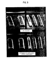
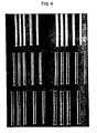
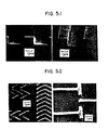
- Poly(4-chlorostyrene), (high fraction), prepared in accordance with Example 1, is dissolved in cyclohexanone to produce an 11% solution.
- a silicon wafer (treated with a drop of hexamethyldichlorosilane) is spin coated (at about 5000 RPM) with the 11% polymer solution to obtain about 7000A thick film after bake.
- the coated silicon support is prebaked at 160°C ⁇ 5°C for 15 minutes and exposed to an electron beam at a base dose of 5ucoul/cm 2 .
- the resist is developed by dipping the irradiated coated support in a solution of 4 parts methylisobutyl ketone (MIBK) to 3 parts 2-ethoxyethanol for at least 3 minutes, then dipping in 2-ethoxyethanol, without allowing to dry for 30 seconds and then spraying with 2-ethoxyethanol for 5 seconds.
- MIBK methylisobutyl ketone
- the so treated wafer is then blow dried with nitrogen gas, and the resist pattern is ready for further processing. If hardening is desired, the wafer is exposed to a deep UV source (low pressure mercury lamp), prior to the next processing step, for 3-5 minutes and is postbaked at 160-200°C.
- MIBK methylisobutyl ketone
Landscapes
- Chemical & Material Sciences (AREA)
- Physics & Mathematics (AREA)
- Health & Medical Sciences (AREA)
- Chemical Kinetics & Catalysis (AREA)
- Medicinal Chemistry (AREA)
- Polymers & Plastics (AREA)
- Organic Chemistry (AREA)
- Spectroscopy & Molecular Physics (AREA)
- General Physics & Mathematics (AREA)
- Photosensitive Polymer And Photoresist Processing (AREA)
- Exposure And Positioning Against Photoresist Photosensitive Materials (AREA)
- Addition Polymer Or Copolymer, Post-Treatments, Or Chemical Modifications (AREA)
Applications Claiming Priority (2)
| Application Number | Priority Date | Filing Date | Title |
|---|---|---|---|
| US37383982A | 1982-05-03 | 1982-05-03 | |
| US373839 | 1995-01-17 |
Publications (2)
| Publication Number | Publication Date |
|---|---|
| EP0093202A1 true EP0093202A1 (fr) | 1983-11-09 |
| EP0093202B1 EP0093202B1 (fr) | 1986-06-04 |
Family
ID=23474101
Family Applications (1)
| Application Number | Title | Priority Date | Filing Date |
|---|---|---|---|
| EP82111811A Expired EP0093202B1 (fr) | 1982-05-03 | 1982-12-20 | Poly-(halostyrène) pour compositions de réserve négatives |
Country Status (3)
| Country | Link |
|---|---|
| EP (1) | EP0093202B1 (fr) |
| JP (1) | JPS58192035A (fr) |
| DE (1) | DE3271595D1 (fr) |
Cited By (3)
| Publication number | Priority date | Publication date | Assignee | Title |
|---|---|---|---|---|
| WO1987002998A1 (fr) * | 1985-11-15 | 1987-05-21 | General Electric Company | Polymerisation cationique de composes aromatiques de bromoalkenyle avec un agent de transfert de chaine aromatique, et produits |
| EP0236914A2 (fr) * | 1986-03-06 | 1987-09-16 | AT&T Corp. | Fabrication d'un dispositif éléctronique par technique lithographique |
| WO2003079112A1 (fr) * | 2002-03-15 | 2003-09-25 | Quantiscript Inc. | Procede de production de structure polymere resistant a la gravure utilisant la lithographie par faisceau d'electrons |
Families Citing this family (5)
| Publication number | Priority date | Publication date | Assignee | Title |
|---|---|---|---|---|
| JPS60116132A (ja) * | 1983-11-29 | 1985-06-22 | Fujitsu Ltd | ネガ型レジストパタ−ンの形成方法 |
| JPS61149947A (ja) * | 1984-12-24 | 1986-07-08 | Nec Corp | レジスト材料 |
| JPS61156253A (ja) * | 1984-12-28 | 1986-07-15 | Nec Corp | レジスト材料 |
| JPS61156254A (ja) * | 1984-12-28 | 1986-07-15 | Nec Corp | レジスト材料 |
| JPS6247049A (ja) * | 1985-08-26 | 1987-02-28 | Hoya Corp | パタ−ン形成方法 |
Citations (2)
| Publication number | Priority date | Publication date | Assignee | Title |
|---|---|---|---|---|
| US3440229A (en) * | 1965-04-05 | 1969-04-22 | Dow Chemical Co | Process for making chlorostyrene copolymers |
| US4201570A (en) * | 1976-12-10 | 1980-05-06 | Scm Corporation | Process for quenching of fine particulates |
-
1982
- 1982-12-20 DE DE8282111811T patent/DE3271595D1/de not_active Expired
- 1982-12-20 EP EP82111811A patent/EP0093202B1/fr not_active Expired
-
1983
- 1983-03-18 JP JP58044619A patent/JPS58192035A/ja active Granted
Patent Citations (2)
| Publication number | Priority date | Publication date | Assignee | Title |
|---|---|---|---|---|
| US3440229A (en) * | 1965-04-05 | 1969-04-22 | Dow Chemical Co | Process for making chlorostyrene copolymers |
| US4201570A (en) * | 1976-12-10 | 1980-05-06 | Scm Corporation | Process for quenching of fine particulates |
Cited By (5)
| Publication number | Priority date | Publication date | Assignee | Title |
|---|---|---|---|---|
| WO1987002998A1 (fr) * | 1985-11-15 | 1987-05-21 | General Electric Company | Polymerisation cationique de composes aromatiques de bromoalkenyle avec un agent de transfert de chaine aromatique, et produits |
| US4755573A (en) * | 1985-11-15 | 1988-07-05 | General Electric Company | Cationic polymerization of bromoalkenyl aromatic compounds with aromatic chain transfer agent, and products |
| EP0236914A2 (fr) * | 1986-03-06 | 1987-09-16 | AT&T Corp. | Fabrication d'un dispositif éléctronique par technique lithographique |
| EP0236914A3 (en) * | 1986-03-06 | 1987-12-02 | American Telephone And Telegraph Company | Fabrication of electronic devices utilizing lithographic techniques |
| WO2003079112A1 (fr) * | 2002-03-15 | 2003-09-25 | Quantiscript Inc. | Procede de production de structure polymere resistant a la gravure utilisant la lithographie par faisceau d'electrons |
Also Published As
| Publication number | Publication date |
|---|---|
| JPS58192035A (ja) | 1983-11-09 |
| DE3271595D1 (de) | 1986-07-10 |
| EP0093202B1 (fr) | 1986-06-04 |
| JPH0234380B2 (fr) | 1990-08-02 |
Similar Documents
| Publication | Publication Date | Title |
|---|---|---|
| US6262181B1 (en) | Preparation of partially cross-linked polymers and their use in pattern formation | |
| EP0017032B1 (fr) | Procédé de fabrication d'un dispositif à l'état solide par décapage différentiel par plasma des couches résistantes | |
| US4433044A (en) | Dry developable positive photoresists | |
| KR100557609B1 (ko) | 신규의 포토레지스트 가교제 및 이를 이용한 포토레지스트 조성물 | |
| JP2001072716A (ja) | 有機金属重合体およびその使用 | |
| US4764247A (en) | Silicon containing resists | |
| US4096290A (en) | Resist mask formation process with haloalkyl methacrylate copolymers | |
| KR100272115B1 (ko) | 평판인쇄법을반도체디바이스를제조하는방법 | |
| EP0093202B1 (fr) | Poly-(halostyrène) pour compositions de réserve négatives | |
| JP2812927B2 (ja) | アセタール基を含有するアルコキシ−スチレン重合体とその製造方法及びアルコキシ−スチレン重合体を主要成分とする化学増幅型フォトレジスト材料 | |
| KR100647379B1 (ko) | 신규의 포토레지스트용 단량체, 그의 공중합체 및 이를 이용한포토레지스트 조성물 | |
| Pawlowski et al. | Modified polyhydroxystyrenes as matrix resins for dissolution inhibition type photoresists | |
| US4678850A (en) | Halogenated polystyrenes for electron beam, X-ray and photo resists | |
| JPS63156812A (ja) | o−ニトロカルビノールエステル基を有する共重合体及びその製造方法 | |
| US4623609A (en) | Process for forming patterns using ionizing radiation sensitive resist | |
| EP0110576B1 (fr) | Matériel sensible aux radiations ionisantes et emploi pour la réalisation de patrons | |
| KR20000034148A (ko) | 신규의 포토레지스트 가교제 및 이를 이용한 포토레지스트 조성물 | |
| JPH0616176B2 (ja) | 製品の製造方法 | |
| JP3031421B2 (ja) | 化学増幅ポジ型レジスト材 | |
| JPS62240953A (ja) | レジスト | |
| US4243742A (en) | Radiation-sensitive positively acting materials | |
| KR100200313B1 (ko) | 신규한 포토레지스트용 공중합체 | |
| JPS58216243A (ja) | 電離放射線感応性材料 | |
| JPH0149928B2 (fr) | ||
| JPS6122340A (ja) | レジスト材料 |
Legal Events
| Date | Code | Title | Description |
|---|---|---|---|
| PUAI | Public reference made under article 153(3) epc to a published international application that has entered the european phase |
Free format text: ORIGINAL CODE: 0009012 |
|
| AK | Designated contracting states |
Designated state(s): DE FR GB |
|
| 17P | Request for examination filed |
Effective date: 19840320 |
|
| GRAA | (expected) grant |
Free format text: ORIGINAL CODE: 0009210 |
|
| AK | Designated contracting states |
Kind code of ref document: B1 Designated state(s): DE FR GB |
|
| REF | Corresponds to: |
Ref document number: 3271595 Country of ref document: DE Date of ref document: 19860710 |
|
| ET | Fr: translation filed | ||
| PLBE | No opposition filed within time limit |
Free format text: ORIGINAL CODE: 0009261 |
|
| STAA | Information on the status of an ep patent application or granted ep patent |
Free format text: STATUS: NO OPPOSITION FILED WITHIN TIME LIMIT |
|
| 26N | No opposition filed | ||
| PGFP | Annual fee paid to national office [announced via postgrant information from national office to epo] |
Ref country code: GB Payment date: 19921126 Year of fee payment: 11 |
|
| PGFP | Annual fee paid to national office [announced via postgrant information from national office to epo] |
Ref country code: DE Payment date: 19921214 Year of fee payment: 11 |
|
| PGFP | Annual fee paid to national office [announced via postgrant information from national office to epo] |
Ref country code: FR Payment date: 19931129 Year of fee payment: 12 |
|
| PG25 | Lapsed in a contracting state [announced via postgrant information from national office to epo] |
Ref country code: GB Effective date: 19931220 |
|
| GBPC | Gb: european patent ceased through non-payment of renewal fee |
Effective date: 19931220 |
|
| PG25 | Lapsed in a contracting state [announced via postgrant information from national office to epo] |
Ref country code: DE Effective date: 19940901 |
|
| PG25 | Lapsed in a contracting state [announced via postgrant information from national office to epo] |
Ref country code: FR Effective date: 19950831 |
|
| REG | Reference to a national code |
Ref country code: FR Ref legal event code: ST |