CN1185698C - 半导体装置及其制造方法、电路板以及电子设备 - Google Patents
半导体装置及其制造方法、电路板以及电子设备 Download PDFInfo
- Publication number
- CN1185698C CN1185698C CNB011432926A CN01143292A CN1185698C CN 1185698 C CN1185698 C CN 1185698C CN B011432926 A CNB011432926 A CN B011432926A CN 01143292 A CN01143292 A CN 01143292A CN 1185698 C CN1185698 C CN 1185698C
- Authority
- CN
- China
- Prior art keywords
- semiconductor device
- wiring
- substrate
- basic substrate
- semiconductor chip
- Prior art date
- Legal status (The legal status is an assumption and is not a legal conclusion. Google has not performed a legal analysis and makes no representation as to the accuracy of the status listed.)
- Expired - Fee Related
Links
- 239000004065 semiconductor Substances 0.000 title claims abstract description 195
- 238000000034 method Methods 0.000 title claims abstract description 32
- 238000004519 manufacturing process Methods 0.000 title claims abstract description 31
- 239000000758 substrate Substances 0.000 claims abstract description 163
- 230000015572 biosynthetic process Effects 0.000 claims description 13
- 239000000463 material Substances 0.000 claims description 13
- 238000007789 sealing Methods 0.000 claims description 8
- 229920005992 thermoplastic resin Polymers 0.000 claims description 6
- 238000010438 heat treatment Methods 0.000 claims description 5
- 238000003825 pressing Methods 0.000 claims description 3
- 238000002844 melting Methods 0.000 abstract description 4
- 230000008018 melting Effects 0.000 abstract description 4
- 229910000679 solder Inorganic materials 0.000 description 21
- 238000010586 diagram Methods 0.000 description 19
- 229920005989 resin Polymers 0.000 description 12
- 239000011347 resin Substances 0.000 description 12
- RYGMFSIKBFXOCR-UHFFFAOYSA-N Copper Chemical compound [Cu] RYGMFSIKBFXOCR-UHFFFAOYSA-N 0.000 description 9
- PXHVJJICTQNCMI-UHFFFAOYSA-N Nickel Chemical compound [Ni] PXHVJJICTQNCMI-UHFFFAOYSA-N 0.000 description 7
- 239000010949 copper Substances 0.000 description 7
- 229910052802 copper Inorganic materials 0.000 description 6
- 230000004907 flux Effects 0.000 description 6
- 239000002245 particle Substances 0.000 description 5
- 229920000106 Liquid crystal polymer Polymers 0.000 description 4
- 239000004977 Liquid-crystal polymers (LCPs) Substances 0.000 description 4
- 239000012768 molten material Substances 0.000 description 4
- ATJFFYVFTNAWJD-UHFFFAOYSA-N Tin Chemical compound [Sn] ATJFFYVFTNAWJD-UHFFFAOYSA-N 0.000 description 3
- 239000011889 copper foil Substances 0.000 description 3
- PCHJSUWPFVWCPO-UHFFFAOYSA-N gold Chemical compound [Au] PCHJSUWPFVWCPO-UHFFFAOYSA-N 0.000 description 3
- 229910052737 gold Inorganic materials 0.000 description 3
- 239000010931 gold Substances 0.000 description 3
- 238000009434 installation Methods 0.000 description 3
- 239000004973 liquid crystal related substance Substances 0.000 description 3
- 229910052759 nickel Inorganic materials 0.000 description 3
- 239000011135 tin Substances 0.000 description 3
- 229910052718 tin Inorganic materials 0.000 description 3
- VYPSYNLAJGMNEJ-UHFFFAOYSA-N Silicium dioxide Chemical compound O=[Si]=O VYPSYNLAJGMNEJ-UHFFFAOYSA-N 0.000 description 2
- 238000005452 bending Methods 0.000 description 2
- 239000007767 bonding agent Substances 0.000 description 2
- 239000011651 chromium Substances 0.000 description 2
- 230000005611 electricity Effects 0.000 description 2
- 239000000155 melt Substances 0.000 description 2
- 238000007747 plating Methods 0.000 description 2
- 229920001187 thermosetting polymer Polymers 0.000 description 2
- 239000010936 titanium Substances 0.000 description 2
- MAKDTFFYCIMFQP-UHFFFAOYSA-N titanium tungsten Chemical compound [Ti].[W] MAKDTFFYCIMFQP-UHFFFAOYSA-N 0.000 description 2
- VYZAMTAEIAYCRO-UHFFFAOYSA-N Chromium Chemical compound [Cr] VYZAMTAEIAYCRO-UHFFFAOYSA-N 0.000 description 1
- BQCADISMDOOEFD-UHFFFAOYSA-N Silver Chemical compound [Ag] BQCADISMDOOEFD-UHFFFAOYSA-N 0.000 description 1
- RTAQQCXQSZGOHL-UHFFFAOYSA-N Titanium Chemical compound [Ti] RTAQQCXQSZGOHL-UHFFFAOYSA-N 0.000 description 1
- 238000010521 absorption reaction Methods 0.000 description 1
- 239000004411 aluminium Substances 0.000 description 1
- 229910052782 aluminium Inorganic materials 0.000 description 1
- XAGFODPZIPBFFR-UHFFFAOYSA-N aluminium Chemical compound [Al] XAGFODPZIPBFFR-UHFFFAOYSA-N 0.000 description 1
- 229910052804 chromium Inorganic materials 0.000 description 1
- 239000011248 coating agent Substances 0.000 description 1
- 238000000576 coating method Methods 0.000 description 1
- 229910052681 coesite Inorganic materials 0.000 description 1
- 239000012141 concentrate Substances 0.000 description 1
- 239000004020 conductor Substances 0.000 description 1
- 229910052906 cristobalite Inorganic materials 0.000 description 1
- 238000007772 electroless plating Methods 0.000 description 1
- 238000010894 electron beam technology Methods 0.000 description 1
- 238000009713 electroplating Methods 0.000 description 1
- 238000005530 etching Methods 0.000 description 1
- 239000000945 filler Substances 0.000 description 1
- 239000011368 organic material Substances 0.000 description 1
- 230000001151 other effect Effects 0.000 description 1
- 238000012856 packing Methods 0.000 description 1
- 229920001721 polyimide Polymers 0.000 description 1
- 239000009719 polyimide resin Substances 0.000 description 1
- 229920000642 polymer Polymers 0.000 description 1
- 238000002360 preparation method Methods 0.000 description 1
- 230000002285 radioactive effect Effects 0.000 description 1
- 239000000377 silicon dioxide Substances 0.000 description 1
- 235000012239 silicon dioxide Nutrition 0.000 description 1
- 229910052709 silver Inorganic materials 0.000 description 1
- 239000004332 silver Substances 0.000 description 1
- 238000005507 spraying Methods 0.000 description 1
- 229910052682 stishovite Inorganic materials 0.000 description 1
- 229910052719 titanium Inorganic materials 0.000 description 1
- 229910052905 tridymite Inorganic materials 0.000 description 1
- XLYOFNOQVPJJNP-UHFFFAOYSA-N water Substances O XLYOFNOQVPJJNP-UHFFFAOYSA-N 0.000 description 1
Images


Classifications
-
- H—ELECTRICITY
- H01—ELECTRIC ELEMENTS
- H01L—SEMICONDUCTOR DEVICES NOT COVERED BY CLASS H10
- H01L23/00—Details of semiconductor or other solid state devices
- H01L23/52—Arrangements for conducting electric current within the device in operation from one component to another, i.e. interconnections, e.g. wires, lead frames
- H01L23/538—Arrangements for conducting electric current within the device in operation from one component to another, i.e. interconnections, e.g. wires, lead frames the interconnection structure between a plurality of semiconductor chips being formed on, or in, insulating substrates
- H01L23/5387—Flexible insulating substrates
-
- H—ELECTRICITY
- H01—ELECTRIC ELEMENTS
- H01L—SEMICONDUCTOR DEVICES NOT COVERED BY CLASS H10
- H01L2224/00—Indexing scheme for arrangements for connecting or disconnecting semiconductor or solid-state bodies and methods related thereto as covered by H01L24/00
- H01L2224/01—Means for bonding being attached to, or being formed on, the surface to be connected, e.g. chip-to-package, die-attach, "first-level" interconnects; Manufacturing methods related thereto
- H01L2224/02—Bonding areas; Manufacturing methods related thereto
- H01L2224/04—Structure, shape, material or disposition of the bonding areas prior to the connecting process
- H01L2224/05—Structure, shape, material or disposition of the bonding areas prior to the connecting process of an individual bonding area
- H01L2224/0554—External layer
- H01L2224/05599—Material
- H01L2224/056—Material with a principal constituent of the material being a metal or a metalloid, e.g. boron [B], silicon [Si], germanium [Ge], arsenic [As], antimony [Sb], tellurium [Te] and polonium [Po], and alloys thereof
- H01L2224/05617—Material with a principal constituent of the material being a metal or a metalloid, e.g. boron [B], silicon [Si], germanium [Ge], arsenic [As], antimony [Sb], tellurium [Te] and polonium [Po], and alloys thereof the principal constituent melting at a temperature of greater than or equal to 400°C and less than 950°C
- H01L2224/05624—Aluminium [Al] as principal constituent
-
- H—ELECTRICITY
- H01—ELECTRIC ELEMENTS
- H01L—SEMICONDUCTOR DEVICES NOT COVERED BY CLASS H10
- H01L2224/00—Indexing scheme for arrangements for connecting or disconnecting semiconductor or solid-state bodies and methods related thereto as covered by H01L24/00
- H01L2224/01—Means for bonding being attached to, or being formed on, the surface to be connected, e.g. chip-to-package, die-attach, "first-level" interconnects; Manufacturing methods related thereto
- H01L2224/02—Bonding areas; Manufacturing methods related thereto
- H01L2224/04—Structure, shape, material or disposition of the bonding areas prior to the connecting process
- H01L2224/05—Structure, shape, material or disposition of the bonding areas prior to the connecting process of an individual bonding area
- H01L2224/0554—External layer
- H01L2224/05599—Material
- H01L2224/056—Material with a principal constituent of the material being a metal or a metalloid, e.g. boron [B], silicon [Si], germanium [Ge], arsenic [As], antimony [Sb], tellurium [Te] and polonium [Po], and alloys thereof
- H01L2224/05638—Material with a principal constituent of the material being a metal or a metalloid, e.g. boron [B], silicon [Si], germanium [Ge], arsenic [As], antimony [Sb], tellurium [Te] and polonium [Po], and alloys thereof the principal constituent melting at a temperature of greater than or equal to 950°C and less than 1550°C
- H01L2224/05647—Copper [Cu] as principal constituent
-
- H—ELECTRICITY
- H01—ELECTRIC ELEMENTS
- H01L—SEMICONDUCTOR DEVICES NOT COVERED BY CLASS H10
- H01L2224/00—Indexing scheme for arrangements for connecting or disconnecting semiconductor or solid-state bodies and methods related thereto as covered by H01L24/00
- H01L2224/01—Means for bonding being attached to, or being formed on, the surface to be connected, e.g. chip-to-package, die-attach, "first-level" interconnects; Manufacturing methods related thereto
- H01L2224/10—Bump connectors; Manufacturing methods related thereto
- H01L2224/12—Structure, shape, material or disposition of the bump connectors prior to the connecting process
- H01L2224/13—Structure, shape, material or disposition of the bump connectors prior to the connecting process of an individual bump connector
- H01L2224/13001—Core members of the bump connector
- H01L2224/13099—Material
- H01L2224/131—Material with a principal constituent of the material being a metal or a metalloid, e.g. boron [B], silicon [Si], germanium [Ge], arsenic [As], antimony [Sb], tellurium [Te] and polonium [Po], and alloys thereof
- H01L2224/13138—Material with a principal constituent of the material being a metal or a metalloid, e.g. boron [B], silicon [Si], germanium [Ge], arsenic [As], antimony [Sb], tellurium [Te] and polonium [Po], and alloys thereof the principal constituent melting at a temperature of greater than or equal to 950°C and less than 1550°C
- H01L2224/13139—Silver [Ag] as principal constituent
-
- H—ELECTRICITY
- H01—ELECTRIC ELEMENTS
- H01L—SEMICONDUCTOR DEVICES NOT COVERED BY CLASS H10
- H01L2224/00—Indexing scheme for arrangements for connecting or disconnecting semiconductor or solid-state bodies and methods related thereto as covered by H01L24/00
- H01L2224/01—Means for bonding being attached to, or being formed on, the surface to be connected, e.g. chip-to-package, die-attach, "first-level" interconnects; Manufacturing methods related thereto
- H01L2224/10—Bump connectors; Manufacturing methods related thereto
- H01L2224/12—Structure, shape, material or disposition of the bump connectors prior to the connecting process
- H01L2224/13—Structure, shape, material or disposition of the bump connectors prior to the connecting process of an individual bump connector
- H01L2224/13001—Core members of the bump connector
- H01L2224/13099—Material
- H01L2224/131—Material with a principal constituent of the material being a metal or a metalloid, e.g. boron [B], silicon [Si], germanium [Ge], arsenic [As], antimony [Sb], tellurium [Te] and polonium [Po], and alloys thereof
- H01L2224/13138—Material with a principal constituent of the material being a metal or a metalloid, e.g. boron [B], silicon [Si], germanium [Ge], arsenic [As], antimony [Sb], tellurium [Te] and polonium [Po], and alloys thereof the principal constituent melting at a temperature of greater than or equal to 950°C and less than 1550°C
- H01L2224/13144—Gold [Au] as principal constituent
-
- H—ELECTRICITY
- H01—ELECTRIC ELEMENTS
- H01L—SEMICONDUCTOR DEVICES NOT COVERED BY CLASS H10
- H01L2224/00—Indexing scheme for arrangements for connecting or disconnecting semiconductor or solid-state bodies and methods related thereto as covered by H01L24/00
- H01L2224/01—Means for bonding being attached to, or being formed on, the surface to be connected, e.g. chip-to-package, die-attach, "first-level" interconnects; Manufacturing methods related thereto
- H01L2224/10—Bump connectors; Manufacturing methods related thereto
- H01L2224/12—Structure, shape, material or disposition of the bump connectors prior to the connecting process
- H01L2224/13—Structure, shape, material or disposition of the bump connectors prior to the connecting process of an individual bump connector
- H01L2224/13001—Core members of the bump connector
- H01L2224/13099—Material
- H01L2224/131—Material with a principal constituent of the material being a metal or a metalloid, e.g. boron [B], silicon [Si], germanium [Ge], arsenic [As], antimony [Sb], tellurium [Te] and polonium [Po], and alloys thereof
- H01L2224/13138—Material with a principal constituent of the material being a metal or a metalloid, e.g. boron [B], silicon [Si], germanium [Ge], arsenic [As], antimony [Sb], tellurium [Te] and polonium [Po], and alloys thereof the principal constituent melting at a temperature of greater than or equal to 950°C and less than 1550°C
- H01L2224/13147—Copper [Cu] as principal constituent
-
- H—ELECTRICITY
- H01—ELECTRIC ELEMENTS
- H01L—SEMICONDUCTOR DEVICES NOT COVERED BY CLASS H10
- H01L2224/00—Indexing scheme for arrangements for connecting or disconnecting semiconductor or solid-state bodies and methods related thereto as covered by H01L24/00
- H01L2224/01—Means for bonding being attached to, or being formed on, the surface to be connected, e.g. chip-to-package, die-attach, "first-level" interconnects; Manufacturing methods related thereto
- H01L2224/10—Bump connectors; Manufacturing methods related thereto
- H01L2224/12—Structure, shape, material or disposition of the bump connectors prior to the connecting process
- H01L2224/13—Structure, shape, material or disposition of the bump connectors prior to the connecting process of an individual bump connector
- H01L2224/13001—Core members of the bump connector
- H01L2224/13099—Material
- H01L2224/131—Material with a principal constituent of the material being a metal or a metalloid, e.g. boron [B], silicon [Si], germanium [Ge], arsenic [As], antimony [Sb], tellurium [Te] and polonium [Po], and alloys thereof
- H01L2224/13138—Material with a principal constituent of the material being a metal or a metalloid, e.g. boron [B], silicon [Si], germanium [Ge], arsenic [As], antimony [Sb], tellurium [Te] and polonium [Po], and alloys thereof the principal constituent melting at a temperature of greater than or equal to 950°C and less than 1550°C
- H01L2224/13155—Nickel [Ni] as principal constituent
-
- H—ELECTRICITY
- H01—ELECTRIC ELEMENTS
- H01L—SEMICONDUCTOR DEVICES NOT COVERED BY CLASS H10
- H01L2224/00—Indexing scheme for arrangements for connecting or disconnecting semiconductor or solid-state bodies and methods related thereto as covered by H01L24/00
- H01L2224/01—Means for bonding being attached to, or being formed on, the surface to be connected, e.g. chip-to-package, die-attach, "first-level" interconnects; Manufacturing methods related thereto
- H01L2224/10—Bump connectors; Manufacturing methods related thereto
- H01L2224/15—Structure, shape, material or disposition of the bump connectors after the connecting process
- H01L2224/16—Structure, shape, material or disposition of the bump connectors after the connecting process of an individual bump connector
- H01L2224/161—Disposition
- H01L2224/16151—Disposition the bump connector connecting between a semiconductor or solid-state body and an item not being a semiconductor or solid-state body, e.g. chip-to-substrate, chip-to-passive
- H01L2224/16221—Disposition the bump connector connecting between a semiconductor or solid-state body and an item not being a semiconductor or solid-state body, e.g. chip-to-substrate, chip-to-passive the body and the item being stacked
- H01L2224/16225—Disposition the bump connector connecting between a semiconductor or solid-state body and an item not being a semiconductor or solid-state body, e.g. chip-to-substrate, chip-to-passive the body and the item being stacked the item being non-metallic, e.g. insulating substrate with or without metallisation
-
- H—ELECTRICITY
- H01—ELECTRIC ELEMENTS
- H01L—SEMICONDUCTOR DEVICES NOT COVERED BY CLASS H10
- H01L2224/00—Indexing scheme for arrangements for connecting or disconnecting semiconductor or solid-state bodies and methods related thereto as covered by H01L24/00
- H01L2224/01—Means for bonding being attached to, or being formed on, the surface to be connected, e.g. chip-to-package, die-attach, "first-level" interconnects; Manufacturing methods related thereto
- H01L2224/26—Layer connectors, e.g. plate connectors, solder or adhesive layers; Manufacturing methods related thereto
- H01L2224/31—Structure, shape, material or disposition of the layer connectors after the connecting process
- H01L2224/32—Structure, shape, material or disposition of the layer connectors after the connecting process of an individual layer connector
- H01L2224/321—Disposition
- H01L2224/32151—Disposition the layer connector connecting between a semiconductor or solid-state body and an item not being a semiconductor or solid-state body, e.g. chip-to-substrate, chip-to-passive
- H01L2224/32221—Disposition the layer connector connecting between a semiconductor or solid-state body and an item not being a semiconductor or solid-state body, e.g. chip-to-substrate, chip-to-passive the body and the item being stacked
- H01L2224/32225—Disposition the layer connector connecting between a semiconductor or solid-state body and an item not being a semiconductor or solid-state body, e.g. chip-to-substrate, chip-to-passive the body and the item being stacked the item being non-metallic, e.g. insulating substrate with or without metallisation
-
- H—ELECTRICITY
- H01—ELECTRIC ELEMENTS
- H01L—SEMICONDUCTOR DEVICES NOT COVERED BY CLASS H10
- H01L2224/00—Indexing scheme for arrangements for connecting or disconnecting semiconductor or solid-state bodies and methods related thereto as covered by H01L24/00
- H01L2224/01—Means for bonding being attached to, or being formed on, the surface to be connected, e.g. chip-to-package, die-attach, "first-level" interconnects; Manufacturing methods related thereto
- H01L2224/42—Wire connectors; Manufacturing methods related thereto
- H01L2224/44—Structure, shape, material or disposition of the wire connectors prior to the connecting process
- H01L2224/45—Structure, shape, material or disposition of the wire connectors prior to the connecting process of an individual wire connector
- H01L2224/45001—Core members of the connector
- H01L2224/45099—Material
-
- H—ELECTRICITY
- H01—ELECTRIC ELEMENTS
- H01L—SEMICONDUCTOR DEVICES NOT COVERED BY CLASS H10
- H01L2224/00—Indexing scheme for arrangements for connecting or disconnecting semiconductor or solid-state bodies and methods related thereto as covered by H01L24/00
- H01L2224/01—Means for bonding being attached to, or being formed on, the surface to be connected, e.g. chip-to-package, die-attach, "first-level" interconnects; Manufacturing methods related thereto
- H01L2224/42—Wire connectors; Manufacturing methods related thereto
- H01L2224/47—Structure, shape, material or disposition of the wire connectors after the connecting process
- H01L2224/48—Structure, shape, material or disposition of the wire connectors after the connecting process of an individual wire connector
- H01L2224/4805—Shape
- H01L2224/4809—Loop shape
- H01L2224/48091—Arched
-
- H—ELECTRICITY
- H01—ELECTRIC ELEMENTS
- H01L—SEMICONDUCTOR DEVICES NOT COVERED BY CLASS H10
- H01L2224/00—Indexing scheme for arrangements for connecting or disconnecting semiconductor or solid-state bodies and methods related thereto as covered by H01L24/00
- H01L2224/01—Means for bonding being attached to, or being formed on, the surface to be connected, e.g. chip-to-package, die-attach, "first-level" interconnects; Manufacturing methods related thereto
- H01L2224/42—Wire connectors; Manufacturing methods related thereto
- H01L2224/47—Structure, shape, material or disposition of the wire connectors after the connecting process
- H01L2224/48—Structure, shape, material or disposition of the wire connectors after the connecting process of an individual wire connector
- H01L2224/481—Disposition
- H01L2224/48151—Connecting between a semiconductor or solid-state body and an item not being a semiconductor or solid-state body, e.g. chip-to-substrate, chip-to-passive
- H01L2224/48221—Connecting between a semiconductor or solid-state body and an item not being a semiconductor or solid-state body, e.g. chip-to-substrate, chip-to-passive the body and the item being stacked
- H01L2224/48225—Connecting between a semiconductor or solid-state body and an item not being a semiconductor or solid-state body, e.g. chip-to-substrate, chip-to-passive the body and the item being stacked the item being non-metallic, e.g. insulating substrate with or without metallisation
- H01L2224/48227—Connecting between a semiconductor or solid-state body and an item not being a semiconductor or solid-state body, e.g. chip-to-substrate, chip-to-passive the body and the item being stacked the item being non-metallic, e.g. insulating substrate with or without metallisation connecting the wire to a bond pad of the item
-
- H—ELECTRICITY
- H01—ELECTRIC ELEMENTS
- H01L—SEMICONDUCTOR DEVICES NOT COVERED BY CLASS H10
- H01L2224/00—Indexing scheme for arrangements for connecting or disconnecting semiconductor or solid-state bodies and methods related thereto as covered by H01L24/00
- H01L2224/01—Means for bonding being attached to, or being formed on, the surface to be connected, e.g. chip-to-package, die-attach, "first-level" interconnects; Manufacturing methods related thereto
- H01L2224/42—Wire connectors; Manufacturing methods related thereto
- H01L2224/47—Structure, shape, material or disposition of the wire connectors after the connecting process
- H01L2224/48—Structure, shape, material or disposition of the wire connectors after the connecting process of an individual wire connector
- H01L2224/484—Connecting portions
- H01L2224/48463—Connecting portions the connecting portion on the bonding area of the semiconductor or solid-state body being a ball bond
- H01L2224/48465—Connecting portions the connecting portion on the bonding area of the semiconductor or solid-state body being a ball bond the other connecting portion not on the bonding area being a wedge bond, i.e. ball-to-wedge, regular stitch
-
- H—ELECTRICITY
- H01—ELECTRIC ELEMENTS
- H01L—SEMICONDUCTOR DEVICES NOT COVERED BY CLASS H10
- H01L2224/00—Indexing scheme for arrangements for connecting or disconnecting semiconductor or solid-state bodies and methods related thereto as covered by H01L24/00
- H01L2224/73—Means for bonding being of different types provided for in two or more of groups H01L2224/10, H01L2224/18, H01L2224/26, H01L2224/34, H01L2224/42, H01L2224/50, H01L2224/63, H01L2224/71
- H01L2224/732—Location after the connecting process
- H01L2224/73201—Location after the connecting process on the same surface
- H01L2224/73203—Bump and layer connectors
- H01L2224/73204—Bump and layer connectors the bump connector being embedded into the layer connector
-
- H—ELECTRICITY
- H01—ELECTRIC ELEMENTS
- H01L—SEMICONDUCTOR DEVICES NOT COVERED BY CLASS H10
- H01L2224/00—Indexing scheme for arrangements for connecting or disconnecting semiconductor or solid-state bodies and methods related thereto as covered by H01L24/00
- H01L2224/73—Means for bonding being of different types provided for in two or more of groups H01L2224/10, H01L2224/18, H01L2224/26, H01L2224/34, H01L2224/42, H01L2224/50, H01L2224/63, H01L2224/71
- H01L2224/732—Location after the connecting process
- H01L2224/73251—Location after the connecting process on different surfaces
- H01L2224/73265—Layer and wire connectors
-
- H—ELECTRICITY
- H01—ELECTRIC ELEMENTS
- H01L—SEMICONDUCTOR DEVICES NOT COVERED BY CLASS H10
- H01L2224/00—Indexing scheme for arrangements for connecting or disconnecting semiconductor or solid-state bodies and methods related thereto as covered by H01L24/00
- H01L2224/74—Apparatus for manufacturing arrangements for connecting or disconnecting semiconductor or solid-state bodies and for methods related thereto
- H01L2224/75—Apparatus for connecting with bump connectors or layer connectors
- H01L2224/7525—Means for applying energy, e.g. heating means
- H01L2224/75251—Means for applying energy, e.g. heating means in the lower part of the bonding apparatus, e.g. in the apparatus chuck
-
- H—ELECTRICITY
- H01—ELECTRIC ELEMENTS
- H01L—SEMICONDUCTOR DEVICES NOT COVERED BY CLASS H10
- H01L2224/00—Indexing scheme for arrangements for connecting or disconnecting semiconductor or solid-state bodies and methods related thereto as covered by H01L24/00
- H01L2224/74—Apparatus for manufacturing arrangements for connecting or disconnecting semiconductor or solid-state bodies and for methods related thereto
- H01L2224/75—Apparatus for connecting with bump connectors or layer connectors
- H01L2224/7525—Means for applying energy, e.g. heating means
- H01L2224/75252—Means for applying energy, e.g. heating means in the upper part of the bonding apparatus, e.g. in the bonding head
-
- H—ELECTRICITY
- H01—ELECTRIC ELEMENTS
- H01L—SEMICONDUCTOR DEVICES NOT COVERED BY CLASS H10
- H01L2224/00—Indexing scheme for arrangements for connecting or disconnecting semiconductor or solid-state bodies and methods related thereto as covered by H01L24/00
- H01L2224/80—Methods for connecting semiconductor or other solid state bodies using means for bonding being attached to, or being formed on, the surface to be connected
- H01L2224/83—Methods for connecting semiconductor or other solid state bodies using means for bonding being attached to, or being formed on, the surface to be connected using a layer connector
- H01L2224/8319—Arrangement of the layer connectors prior to mounting
- H01L2224/83192—Arrangement of the layer connectors prior to mounting wherein the layer connectors are disposed only on another item or body to be connected to the semiconductor or solid-state body
-
- H—ELECTRICITY
- H01—ELECTRIC ELEMENTS
- H01L—SEMICONDUCTOR DEVICES NOT COVERED BY CLASS H10
- H01L2224/00—Indexing scheme for arrangements for connecting or disconnecting semiconductor or solid-state bodies and methods related thereto as covered by H01L24/00
- H01L2224/80—Methods for connecting semiconductor or other solid state bodies using means for bonding being attached to, or being formed on, the surface to be connected
- H01L2224/83—Methods for connecting semiconductor or other solid state bodies using means for bonding being attached to, or being formed on, the surface to be connected using a layer connector
- H01L2224/838—Bonding techniques
- H01L2224/8385—Bonding techniques using a polymer adhesive, e.g. an adhesive based on silicone, epoxy, polyimide, polyester
- H01L2224/83855—Hardening the adhesive by curing, i.e. thermosetting
- H01L2224/83856—Pre-cured adhesive, i.e. B-stage adhesive
-
- H—ELECTRICITY
- H01—ELECTRIC ELEMENTS
- H01L—SEMICONDUCTOR DEVICES NOT COVERED BY CLASS H10
- H01L24/00—Arrangements for connecting or disconnecting semiconductor or solid-state bodies; Methods or apparatus related thereto
- H01L24/01—Means for bonding being attached to, or being formed on, the surface to be connected, e.g. chip-to-package, die-attach, "first-level" interconnects; Manufacturing methods related thereto
- H01L24/42—Wire connectors; Manufacturing methods related thereto
- H01L24/47—Structure, shape, material or disposition of the wire connectors after the connecting process
- H01L24/48—Structure, shape, material or disposition of the wire connectors after the connecting process of an individual wire connector
-
- H—ELECTRICITY
- H01—ELECTRIC ELEMENTS
- H01L—SEMICONDUCTOR DEVICES NOT COVERED BY CLASS H10
- H01L2924/00—Indexing scheme for arrangements or methods for connecting or disconnecting semiconductor or solid-state bodies as covered by H01L24/00
- H01L2924/0001—Technical content checked by a classifier
- H01L2924/00014—Technical content checked by a classifier the subject-matter covered by the group, the symbol of which is combined with the symbol of this group, being disclosed without further technical details
-
- H—ELECTRICITY
- H01—ELECTRIC ELEMENTS
- H01L—SEMICONDUCTOR DEVICES NOT COVERED BY CLASS H10
- H01L2924/00—Indexing scheme for arrangements or methods for connecting or disconnecting semiconductor or solid-state bodies as covered by H01L24/00
- H01L2924/01—Chemical elements
- H01L2924/01078—Platinum [Pt]
-
- H—ELECTRICITY
- H01—ELECTRIC ELEMENTS
- H01L—SEMICONDUCTOR DEVICES NOT COVERED BY CLASS H10
- H01L2924/00—Indexing scheme for arrangements or methods for connecting or disconnecting semiconductor or solid-state bodies as covered by H01L24/00
- H01L2924/01—Chemical elements
- H01L2924/01079—Gold [Au]
-
- H—ELECTRICITY
- H01—ELECTRIC ELEMENTS
- H01L—SEMICONDUCTOR DEVICES NOT COVERED BY CLASS H10
- H01L2924/00—Indexing scheme for arrangements or methods for connecting or disconnecting semiconductor or solid-state bodies as covered by H01L24/00
- H01L2924/15—Details of package parts other than the semiconductor or other solid state devices to be connected
- H01L2924/181—Encapsulation
Landscapes
- Physics & Mathematics (AREA)
- Condensed Matter Physics & Semiconductors (AREA)
- General Physics & Mathematics (AREA)
- Engineering & Computer Science (AREA)
- Computer Hardware Design (AREA)
- Microelectronics & Electronic Packaging (AREA)
- Power Engineering (AREA)
- Wire Bonding (AREA)
- Electric Connection Of Electric Components To Printed Circuits (AREA)
Abstract
提供可以用少数工序安装半导体芯片的半导体装置及其制造方法,电路板以及电子设备。一种半导体装置的制造方法,包括在布线24形成于基本衬底22所构成的布线衬底20上搭载半导体芯片10的工序,在熔化基本衬底22的同时压入半导体芯片10上设有的凸缘14,并使凸缘14与布线24形成电连接。
Description
技术领域
本发明涉及半导体装置及其制造方法、电路板及电子设备。
现有技术
作为CSP(Chip Scale/Size Package)型半导体装置的一种形态,公知的有在衬底上面朝下安装(倒装片连接)了的构造。
此种情况下,在半导体芯片和衬底之间作为底层充填材料多是预备树脂。树脂或是注入到安装后的半导体芯片与衬底之间,或是安装前预先涂布于衬底上。可是,单是准备树脂的过程就要浪费一个工序,所以会增加半导体装置的制造工序。
另外,随着近年来多片组件的开发,在布线衬底的两面安装半导体芯片的形式被开发出来。可是,为此需要在衬底的两面形成布线,进而还需要导电通两面的布线用的导孔,所以在成本的增加和制造工序方面处于劣势。
本发明就是为了解决这一问题点而提出的,其目的在于提供由少的工序就可实装半导体芯片的半导体装置及其制造方法、电路板以及电子设备。
发明内容
(1)本发明所涉及的半导体装置的制造方法,包括在布线衬底上搭载半导体芯片的工序,此布线衬底是在基本衬底上形成布线而构成的,其中边熔化所述基本衬底边压入设置在所述半导体芯片上的凸缘,并使所述凸缘与所述布线电连接。
根据本发明,可在熔化基本衬底的同时压入半导体芯片上设置的凸缘,并使凸缘与布线电连接。因此,例如在具有在基本衬底的一面形成了的布线的布线衬底上,可以简单地在其两面搭载半导体芯片。而且,例如,由于用熔化了的基本衬底材料可以对凸缘等形成密封,所以可以用少量的工序制造出可靠性高的半导体装置。
(2)在此半导体装置的制造方法中,所述布线具有与所述凸缘的电连接部,在所述电连接工序中,可以熔化所述基本衬底而用其材料密封所述凸缘和所述连接部。
据此,可以在一个工序中进行凸缘和布线的连接部的电连接,并对其进行密封。
(3)在此半导体装置的制造方法中,可以在所述电连接工序中,熔化所述基本衬底而使其材料与所述半导体芯片的表面紧密结合。
据此,由于熔化了的基本衬底材料紧密结合在半导体芯片的表面上,所以可以吸收基本衬底对半导体芯片附加的应力。
(4)在此半导体装置的制造方法中,可以在所述电连接工序中,对所述基本衬底加热使其熔化。
据此,例如可以用使凸缘与布线电连接用的热量熔化基本衬底,所以可以简单地熔化基本衬底。
(5)在此半导体装置的制造方法中,作为所述基本衬底可以使用热塑性树脂。
据此,通过加热就容易进行再加工。
(6)在此半导体装置的制造方法中,可以在所述电连接工序中,用夹具固定所述半导体芯片,并对所述夹具进行加热而使所述半导体芯片的至少是所述凸缘部位被加热,并通过向所述基本衬底压靠所述夹具将所述凸缘埋入所述基本衬底中。
(7)在此半导体装置的制造方法中,还可以包括在所述布线衬底上搭载其他半导体芯片的工序。
(8)本发明所涉及的半导体装置可以通过所述制造方法来制造。
(9)本发明所涉及的半导体装置,含有
半导体芯片,具有电极,并在所述电极上形成凸缘;
布线衬底,搭载所述半导体芯片,并在基本衬底上形成具有与所述凸缘的电连接部的布线,
所述凸缘埋入所述基本衬底并与所述布线电连接,
所述凸缘和所述连接部被所述基本衬底密封。
根据本发明,由基本衬底对凸缘和连接部形成密封,所以与布线衬底不同,不一定需要填充密封用树脂,因而可以减少装置的零件数量。另外,由于凸缘埋入在基本衬底中从而可以使半导体装置变得更薄。
(10)在此半导体装置中,可以使所述基本衬底与所述半导体芯片的面紧密结合。
据此,可以吸收基本衬底对所述半导体芯片产生的应力。
(11)在此半导体装置中,所述基本衬底可以是热塑性树脂。
(12)在此半导体装置中,还可以含有搭载于所述布线衬底上的其他半导体芯片。
(13)本发明所涉及的电路板搭载有所述半导体装置。
(14)本发明所涉及的电子设备具有所述半导体装置。
附图说明
图1A~图1C为应用了本发明的第1实施方式所涉及的半导体装置及其制造方法的示意图。
图2为应用了本发明的第2实施方式所涉及的半导体装置的示意图。
图3为应用了本发明的第2实施方式所涉及的半导体装置的制造方法示意图。
图4为应用了本发明的第3实施方式所涉及的半导体装置第1例的示意图。
图5为应用了本发明的第3实施方式所涉及的半导体装置第2例的示意图。
图7为应用了本发明的第3实施方式所涉及的半导体装置第3例的示意图。
图8为应用了本发明的第3实施方式所涉及的半导体装置第4例的示意图。
图9为搭载应用了本发明的实施方式所涉及的半导体装置的电路板的示意图。
图10为具有应用了本发明的实施方式所涉及的半导体装置的电子设备的示意图。
图11为具有应用了本发明的实施方式所涉及的半导体装置的电子设备的示意图。
符号说明
10 半导体芯片
12 电极
14 凸缘
20 布线衬底
22 基本衬底
24 布线
26 连接部
30 夹具
实施方式
下面就本发明的最佳实施方式参照附图加以说明。但是,本发明并不局限于以下的实施方式。
(第一实施方式)
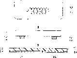
图1A~图1C为应用了本发明的第1实施方式所涉及的半导体装置的制造方法示意图。本实施方式使用半导体芯片10和布线衬底20。
半导体芯片10的形状可以是长方体(包含立方体),也可以是球状。半导体芯片10具有多个电极12。电极12是在半导体芯片10上所形成的电路元件的外部电极,是用铝或铜等形成的既平又薄的嵌片。电极12多形成在半导体芯片10的任意一面上。电极12,可以形成在半导体芯片10的面上形成电路元件的工作区的内侧,也可以形成于其外侧。
电极12可以形成在半导体芯片10的面的端部。电极12也可以形成于半导体芯片10的平行的两边或四边。避开电极12的至少一部分而在半导本芯片10上形成着钝化膜(图中未示)。钝化膜可以由例如SiO2、SiN、聚酰亚胺树脂等形成。
各电极12上设置有凸缘14。凸缘14可以由金、镍、铜、银、锡等至少其中一种材料形成。凸缘14的表面可以电镀。凸缘14可以焊剂电镀。凸缘14的形状不特别限定,可以压成扁平状,可以形成突起,或者是球状也行。凸缘14的高度不特别限定。凸缘14可以通过电电镀或者化学电镀形成,也可以用焊丝熔化成球状而形成。附图示例中凸缘14是1段结构,也可以不同于此而是多段结构。
布线衬底20包括基本衬底和形成于基本衬底22上的复数布线24。复数布线24固定在基本衬底22上,例如可以形成于基本衬底22的某一面。布线衬底20可以是布线24依靠粘接剂(图中未示)形成在基本衬底22上构成三层衬底,也可以是布线24不用粘接剂直接形成在基本衬底22上构成二层衬底。
布线24是指至少实现两处的电连接的部分,独立形成的复数布线24可以称为布线图形。布线24可以是铜(Cu)、铬(Cr)、钛(Ti)、镍(Ni)、钛钨合金(Ti-W)的其中一种材料迭层或者单层形成。这时,布线24最好用焊剂、锡、金、镍等进行电镀。布线24可以通过蚀刻、电镀处理或者喷镀等形成。例如,可以通过加热和加压使铜箔贴在基本衬底22上,再通过光学蚀刻法形成铜图形,然后用锡或金等电镀而形成布线24。
布线24具有复数的连接部26。连接部26是用于与半导体芯片10进行电连接的布线24的一部分。连接部26与凸缘14形成电连接。连接部26可以是焊接区。连接部26可以用焊剂等电镀以形成良好的连接。
基本衬底22最好是以有机材料形成。基本衬底22最好以含有树脂的材料形成。基本衬底22也可以是热塑性树脂。依靠热塑性树脂,一旦加工成布线衬底20之后可以容易地进行再次加工。或者,基本衬底22也可以是热硬化性树脂。热硬化性树脂可以在半硬化状态时固定布线24,进行再次加工。
基本衬底22也可以在树脂中含有导电粒子(图中未示)。基本衬底22还可以是各向异性导电薄膜(ACF)。凸缘14通过导电粒子与连接部26形成电连接。使用各向异性导电薄膜,导电粒子只在受挤压的方向上导通电流,其他方向上则不导通。因此,即使在各向异性导电薄膜上固定复数布线24,各布线24之间也不会形成电流导通。
基本衬底22也可以使用液晶聚合物(LCP)。液晶聚合物在熔化时呈现液晶状态。与其他聚合物相比,其具有尺寸变化不易受温度和湿度影响的特征。
例如,布线衬底20可以采用在液晶聚合物薄膜BIAC(注册商标)上形成铜箔(布线24)的软铜箔迭层板。这样,其吸水率很低,即使在高湿度的环境下也可以保持其尺寸的高度稳定性。另外,其热膨胀系数被设定为与铜箔(布线24)大致相同的数值,所以不会由于温度变化而发生翘曲。
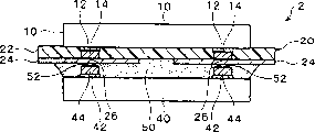
如图1A所示,半导体芯片10与基本衬底20相对。如图所示,在使用一侧表面具有布线24的布线衬底20时,使布线衬底20的另一侧表面与半导体芯片10相对。半导体芯片10上形成电极12的面朝向布线衬底20。半导体芯片10采用所谓的面朝下安装。
半导体芯片10的各凸缘14与布线24的各连接部26对准位置。例如可使布线衬底20置于图中未示的平台上,用夹具30固定半导体芯片10对准位置。夹具30也可以吸附于半导体芯片10的形成了电极12的一侧相对的面上加以固定。本图示例中夹具30内部具有通过热源进行供热的加热器32。
接下来,如图1B所示,在使基本衬底22熔化的同时将半导体芯片10的凸缘14压入到基本衬底22中。换言之,就是在将半导体芯片10的凸缘14压入基本衬底22的同时熔化基本衬底22。
熔化基本衬底22所施加的能量可以与基本衬底22发生熔化的机械特性相对应。该能量可以是放射线(包括可见光、紫外线、电子束、X射线等)和热能等。图中示例是依靠热能使基本衬底20熔化的,这时可以通过夹具30的加热器32加热基本衬底22使其熔化。加热器32至少要加热半导体芯片10的凸缘14。
为了压入半导体芯片10的凸缘14,至少要使半导体芯片10或基本衬底22的其中一方向另一方进行挤压。例如,可以使夹具30压靠于半导体芯片10并向基本衬底22进行挤压。如使用夹具30,可以同时进行熔化基本衬底22和压入半导体芯片10的凸缘14。
这样,如图1C所示,凸缘14被埋入到熔化的基本衬底22中并与布线24形成电连接。据此,与不熔化基本衬底22而机械性地将凸缘14压入到基本衬底22中相比,仅用较小的压力就可使凸缘14与布线24形成电连接。另外,由于熔化了基本衬底22,凸缘14可以推挤基本衬底22的熔化材料而更确实地抵达连接部26。
凸缘14和连接部26可以被基本衬底密封。具体说就是基本衬底22的熔化材料紧密结合于凸缘14和连接部26的周围。基本衬底22的熔化材料在凸缘1 4与连接部26形成电连接时,在其周围的缝隙间流动以填满其缝隙。据此,可以防止电短路,也可提高装置的防潮性能。
另外,半导体芯片10的面可以与基本衬底22紧密结合。也就是说,半导体芯片10可以被压入基本衬底22,基本衬底22的熔化材料与半导体芯片10的面紧密结合。本图示例中,基本衬底22紧密结合于半导体芯片10形成电极12的面。另外,半导体芯片10的一部分可以被埋入于基本衬底22中,也可以不埋入。
据此,半导体芯片10和布线26之间能够形成被树指等的基本衬底22的材料紧密充填的状态。因此,集中于各凸缘14(或者是布线24的各连接部26)的应力能够通过基本衬底22被分散于半导体芯片10的整个面上。就是说半导体芯片10受到的应力可以被基本衬底22所吸收。
另外,基本衬底22的厚度可以大于凸缘14从半导体芯片10具有电极12的面上所突出的厚度。据此,便于使半导体芯片10的一部分埋入基本衬底22中而使半导体芯片10与基本衬底22紧密结合。
下面就本实施方式所涉及的半导体装置进行说明。不过,在以下说明中省略与制造方法中所作的说明内容相重复的记载。
如图1C所示,半导体装置中1包括具有复数电极12并在各电极12上形成凸缘14的半导体芯片10以及在基本衬底22上形成具有与凸缘14的电连接部26的复数布线24所构成的布线衬底20。本图示例中,基本衬底22的一面形成布线24。换言之,布线衬底20具有基本衬底22侧的面和布线24侧的面。
本图示例中,半导体芯片10被搭载于布线衬底20的基本衬底22侧的面上。而且,凸缘14埋入于基本衬底22中与布线24形成电连接。凸缘14在位于与基本衬底22上具有半导体芯片10的面相反一侧面的位置与连接部26形成连接。也就是说,凸缘14贯穿基本衬底22。半导体芯片10以所谓的面朝下方式被安装于布线24上。
凸缘14和连接部26被基本衬底22所密封。也就是说,基本衬底22的固化材料与二者紧密结合。另外,基本衬底22可以紧密结合于半导体芯片10具有电极12的面上。本图示例中,基本衬底22的面在半导体芯片10的外侧成为平面,但也可以不同于此使其覆盖半导体芯片10的端部的至少一部分而形成隆起。
据此,凸缘14和连接部26被基本衬底22密封,所以与布线衬底20不同,不一定需要填充密封用的树脂,因而可以减少装置的零件数量。另外,由于凸缘14埋入在基本衬底22中,因而可以使半导体装置变得更薄。
本实施方式所涉及的半导体装置的封装形式可以称之为BGA(BallGrid Array)或CSP(Chip Size/Scale Package)。并且,布线衬底20可以采用COF(Chip On Flex/Film)用板和COB(Chip On Board)用板。
(第2实施方式)
图2和图3是应用了本发明的第2实施方式所涉及的半导体装置的示意图。在本实施方式中对把所述半导体芯片的安装方式应用于多片组件形成所得到的半导体装置及其制造方法的一例进行说明。并且,在以下说明中可以尽可能地应用第一实施方式的说明内容。
半导体装置2包括第1个和第2个半导体芯片10、40以及布线衬底20。第1个半导体芯片10与已经说明过的内容相同,第2个半导体芯片40具有复数的电极42,各电极12上形成凸缘44。另外,本图示例中布线衬底20是在基本衬底22的一面形成布线24。
第2个半导体芯片40被面朝下安装于布线衬底20的布线24侧的面上。如图2所示,第2个半导体芯片40可以通过含有导电粒子52的各向异性导电材料50结合于布线衬底20上。这时,凸缘44通过导电粒子52与布线24形成电连接。
第2个半导体芯片40可以是与第1个半导体芯片相对应的镜像芯片。而且,各凸缘44可以连接于与第一个半导体芯片10的各凸缘14形成电连接的连接部26的位置。
据此,例如当第1个和第2个半导体芯片10、40为存储器的时候,可以通过同一排列的外部端子(图中未示)在各自存储器的相同地址的存储单元上进行信息的读出和写入。另外,仅通过芯片选择端子的连接就可以分开第1个和第2个半导体芯片10、40,据此能够利用同一外部端子的排列分别控制至少两个(可以是多数)半导体芯片。
本实施方式所涉及的半导体装置中,第2个半导体芯片40可以搭载于布线24所形成的面,所以可以简单地在两面安装半导体芯片10,40。而且,由于第1个半导体芯片10的凸缘14埋入到基本衬底22中,所以可以使半导体装置2变得更薄。因此可以提供低成本的且是小型的多片组件。
图3是本实施方式所涉及的半导体装置制造方法的示意图。第1个和第2个半导体芯片10,40可以分别搭载于布线衬底20上,也可以大致同时搭载。
当第1个和第2个半导体芯片10,40在大致同是搭载时,可以从布线24的连接部26的两侧施加压力,所以不必对布线24施加格外的压力。而且,同时搭载可以减少搭载时间,因而可以提高生产效率。
当第1个和第2个半导体芯片10,40分别搭载时,可以先搭载第1个半导体芯片10。这样可以在确认凸缘14与连接部26连接良好之后,搭载第2个半导体芯片40,从而可以减少连接不良的发生。
(第3实施方式)
图4-图8为应用了本发明的第3实施方式所涉及的半导体装置的示意图。本实施方式中将说明把第1实施方式所阐述的半导体芯片的安装方式应用于多片组件形式所得到的半导体装置。并且,在以下说明中可以尽可能应用所述实施方式中的说明内容。
(第1例)
图4为本实施方式所涉及的半导体装置的第1例的示意图。半导体装置3包括第1个和第2个半导体芯片10,60以及布线衬底20。本第1例与第2实施方式的示例的区别在于第1个和第2个半导体芯片10,6(的外形互不相同。
第2个半导体芯片60可以比第1个半导体芯片10的外形大也可以比其小。各电极62上的凸缘64在与第1个半导体芯片10的凸缘14所连接的连接部26不同的位置的连接部28与布线24形成电连接。
本图示例中省略了布线衬底20的外部端子。外部端子连接于图中未示的电路部件(例如液晶面板和主插件板)。例如可以延伸布线衬底的一部分设法进行外部连接。也就是说,可以把固定在基本衬底22上的布线24的一部份作为插接件的引线。
(第2例)
图5为本实施方式所涉及的半导体装置第2例的示意图。半导体装置4包括第1个和第2个半导体芯片10,70,第2个半导体芯片70以树脂76密封。
第2个半导体芯片70面朝上安装于布线衬底20上。电极72通过导线74与连接部28相连接。树脂76可以采用使用模具制造的模压树脂。另外,本图示例中也省略了布线衬底20的外部端子。
(第3例)
图6和图7为本实施方式所涉及的半导体装置第3例的示意图。半导体装置5包括第1个和第2个半导体芯片10,40以及布线衬底20。作为外部端子,在布线衬底20上设有复数的焊剂球80。
布线衬底20具有搭载第1个和第2个半导体芯片10,40的区域和设置复数的焊剂球80的区域。因为各区域分别设置,所以在制造工序中可以控制对半导体芯片等施压的压力。各半导体芯片的搭载区域的大小可以与焊剂球80的搭载区域大致相同。这样可以使两区域重叠。
另外,相对于设置焊剂球80的一个区域,搭载半导体芯片的区域可以设为两个以上。搭载了半导体芯片的各区域可以从复数方向褶积,因而可以制造出平面面积与设置焊剂球80的区域面积大致相同的半导体装置。
焊剂球80可以如图所示突出于布线衬底20的基本衬底22侧,也可以突出于布线衬底20的布线22侧。突出于基本衬底22侧时,焊剂球80通过基本衬底22的贯穿孔23突出。贯穿孔23形成于与布线24相重的部分。焊剂球80可以将预先形成的焊剂置于布线24的一部分即焊接区25上通过回流工序形成。
或者不积极地设置焊剂球,可以通过在电路部件上涂布焊剂而结果性地形成焊剂球80。另外,在焊剂球80的设置区域也可以搭载半导体芯片(图中未示)。
图7所示的半导体装置6是由半导体装置5弯曲而成的。具体说是将各半导体芯片10,40所搭载的区域与焊剂球80的设置区域重叠并使该焊剂球80向外侧突出。据此,可以提供小型且高密度的半导体装置。
(第4例)
图8为本实施方式所涉及的半导体装置第4例的示意图。半导体装置7的布线24的一部分形成弯曲部90而构成复数的外部端子。
弯曲部90从基本衬底22的面突出。具体说是布线24在从基本衬底22突出方向的前端部位形成弯曲。基本衬底22上弯曲部90所在的位置可以形成贯穿孔92。这样,可以使具有凸状部位的夹具穿过贯穿孔92在布线24上形成凸状的弯曲部90。
图8中,弯曲部90向布线衬底20的布线24侧突出,但也可以通过贯穿孔92向基本衬底22侧突出。由于利用布线24的一部分构成外部端子,所以可以减少半导体装置的零件数量。
弯曲部90可以在布线24的一部分(例如焊接区)使中央部位突起而形成。此时弯曲部90的内侧可以充填导电膏等。由于外部端子是利用比焊剂硬的布线24(例如铜)形成的,从而可以提高装置的温度周期可靠性能。
另外,本例可以应用到所述具有焊剂球80的所有的实施方式中以替换焊剂球80。
根据所述多片组件的形式,由于第1个半导体芯片10搭载于布线衬底20的基本衬底22侧,所以在形成布线24侧可以以各种方式简单地安装其他半导体芯片(第2个半导体芯片60,70)。而且,由于半导体芯片10的凸缘14埋入在基本衬底22中而可以使半导体装置更趋小型化。其他效果如同在所述实施方式中所阐述的一样。
图9为应用了本发明的实施方式所涉及的电路板的示意图。如图9所示,所述的半导体装置与电路板形成电连接。电路板可以是液晶面板100。半导体装置1制成将带状半导体装置的基本衬底22按围绕复数布线24的轮廓切割成的形状。
作为具有应用了本发明的半导体装置的电子设备,图10示出笔记本式个人电脑200。图11示出移动电话300。该移动电话300也具有应用了本发明的电路板(液晶面板100)。
Claims (16)
1.一种半导体装置的制造方法,包括在布线衬底上搭载半导体芯片的工序,此布线衬底是在由含树脂的材料构成的基本衬底上形成布线而构成的,其中,
把所述半导体芯片搭载在所述基本衬底中所述布线的形成面的相反面上,边熔化所述基本衬底边压入设置在所述半导体芯片上的凸缘,并使所述凸缘与所述布线电连接。
2.权利要求1记载的半导体装置的制造方法,其中,
所述布线具有与所述凸缘的电连接部,
在所述电连接工序中,熔化所述基本衬底,用其材料对所述凸缘和所述连接部进行密封。
3.权利要求1记载的半导体装置的制造方法,其中,
在所述电连接工序中,熔化所述基本衬底,并使其材料与所述半导体芯片的面紧密结合。
4.权利要求1记载的半导体装置的制造方法,其中,
在所述电连接工序中,通过加热熔化所述基本衬底。
5.权利要求1记载的半导体装置的制造方法,其中,
作为所述基本衬底使用热塑性树脂。
6.权利要求1记载的半导体装置的制造方法,其中,
在所述电连接工序中,用夹具固定所述半导体芯片,通过加热所述夹具至少加热所述半导体芯片的所述凸缘,并通过向所述基本衬底压靠所述夹具将所述凸缘埋入所述基本衬底中。
7.权利要求1至权利要求6之一记载的半导体装置的制造方法,其中,
还包括在所述布线衬底上搭载其他半导体芯片的工序。
8.一种半导体装置,其根据权利要求1至权利要求6之一记载的制造方法制成。
9.一种半导体装置,包括
半导体芯片,具有电极,并在所述电极上形成凸缘;
布线衬底,在由含树脂的材料构成的基本衬底上形成具有与所述凸缘的电连接部的布线,
所述半导体芯片搭载在所述基本衬底中所述布线的形成面的相反面上,
所述凸缘埋入所述基本衬底并与所述布线电连接,
所述凸缘和所述连接部被所述基本衬底密封。
10.权利要求9记载的半导体装置,其中,
所述基本衬底与所述半导体芯片的面紧密结合。
11.权利要求9记载的半导体装置,其中,
所述基本衬底是热塑性树脂。
12.权利要求9记载的半导体装置,其中,
还包括搭载于所述布线衬底上的其他半导体芯片。
13.一种电路板,其搭载了权利要求8记载的半导体装置。
14.一种电路板,其搭载了权利要求9至权利要求12的任意一项记载的半导体装置。
15.一种电子设备,其具有权利要求8记载的半导体装置。
16.一种电子设备,其具有权利要求9至权利要求12的任意一项记载的半导体装置。
Applications Claiming Priority (3)
| Application Number | Priority Date | Filing Date | Title |
|---|---|---|---|
| JP2000395111A JP2002198395A (ja) | 2000-12-26 | 2000-12-26 | 半導体装置及びその製造方法、回路基板並びに電子機器 |
| JP395111/2000 | 2000-12-26 | ||
| JP395111/00 | 2000-12-26 |
Publications (2)
| Publication Number | Publication Date |
|---|---|
| CN1362733A CN1362733A (zh) | 2002-08-07 |
| CN1185698C true CN1185698C (zh) | 2005-01-19 |
Family
ID=18860628
Family Applications (1)
| Application Number | Title | Priority Date | Filing Date |
|---|---|---|---|
| CNB011432926A Expired - Fee Related CN1185698C (zh) | 2000-12-26 | 2001-12-26 | 半导体装置及其制造方法、电路板以及电子设备 |
Country Status (3)
| Country | Link |
|---|---|
| US (1) | US6846699B2 (zh) |
| JP (1) | JP2002198395A (zh) |
| CN (1) | CN1185698C (zh) |
Families Citing this family (24)
| Publication number | Priority date | Publication date | Assignee | Title |
|---|---|---|---|---|
| SG122743A1 (en) * | 2001-08-21 | 2006-06-29 | Micron Technology Inc | Microelectronic devices and methods of manufacture |
| JP3914431B2 (ja) * | 2001-12-26 | 2007-05-16 | 松下電器産業株式会社 | 半導体装置の製造方法 |
| US20030132528A1 (en) * | 2001-12-28 | 2003-07-17 | Jimmy Liang | Method and apparatus for flip chip device assembly by radiant heating |
| SG104293A1 (en) * | 2002-01-09 | 2004-06-21 | Micron Technology Inc | Elimination of rdl using tape base flip chip on flex for die stacking |
| US6975035B2 (en) * | 2002-03-04 | 2005-12-13 | Micron Technology, Inc. | Method and apparatus for dielectric filling of flip chip on interposer assembly |
| SG115456A1 (en) * | 2002-03-04 | 2005-10-28 | Micron Technology Inc | Semiconductor die packages with recessed interconnecting structures and methods for assembling the same |
| SG121707A1 (en) * | 2002-03-04 | 2006-05-26 | Micron Technology Inc | Method and apparatus for flip-chip packaging providing testing capability |
| SG115455A1 (en) * | 2002-03-04 | 2005-10-28 | Micron Technology Inc | Methods for assembly and packaging of flip chip configured dice with interposer |
| SG115459A1 (en) * | 2002-03-04 | 2005-10-28 | Micron Technology Inc | Flip chip packaging using recessed interposer terminals |
| SG111935A1 (en) | 2002-03-04 | 2005-06-29 | Micron Technology Inc | Interposer configured to reduce the profiles of semiconductor device assemblies and packages including the same and methods |
| US6791168B1 (en) * | 2002-07-10 | 2004-09-14 | Micron Technology, Inc. | Semiconductor package with circuit side polymer layer and wafer level fabrication method |
| US20040036170A1 (en) * | 2002-08-20 | 2004-02-26 | Lee Teck Kheng | Double bumping of flexible substrate for first and second level interconnects |
| TW591780B (en) * | 2003-03-21 | 2004-06-11 | Univ Nat Central | Flip chip Au bump structure and method of manufacturing the same |
| DE10339609A1 (de) * | 2003-08-28 | 2005-03-24 | Forschungszentrum Karlsruhe Gmbh | Oligonukleotid, Verfahren und System zur Detektion von Antibiotikaresistenz-vermittelnden Genen in Mikroorganismen mittels der Echtzeit-PCR |
| JP4593951B2 (ja) * | 2004-03-29 | 2010-12-08 | ルネサスエレクトロニクス株式会社 | マルチチップパッケージの製造方法 |
| FR2875995B1 (fr) * | 2004-09-24 | 2014-10-24 | Oberthur Card Syst Sa | Procede de montage d'un composant electronique sur un support, de preference mou, et entite electronique ainsi obtenue, telle q'un passeport |
| JP2006210566A (ja) * | 2005-01-27 | 2006-08-10 | Akita Denshi Systems:Kk | 半導体装置 |
| JP4654865B2 (ja) | 2005-09-30 | 2011-03-23 | パナソニック株式会社 | 電子部品実装方法 |
| GB0705287D0 (en) * | 2007-03-20 | 2007-04-25 | Conductive Inkjet Tech Ltd | Electrical connection of components |
| JP4952353B2 (ja) * | 2007-04-18 | 2012-06-13 | パナソニック株式会社 | チップモジュールおよびメモリカード |
| JP2011109046A (ja) * | 2009-11-20 | 2011-06-02 | Sony Chemical & Information Device Corp | 実装装置および電子モジュールの製造方法 |
| US9252130B2 (en) * | 2013-03-29 | 2016-02-02 | Stats Chippac, Ltd. | Methods of manufacturing flip chip semiconductor packages using double-sided thermal compression bonding |
| US10147702B2 (en) * | 2016-10-24 | 2018-12-04 | Palo Alto Research Center Incorporated | Method for simultaneously bonding multiple chips of different heights on flexible substrates using anisotropic conductive film or paste |
| US20220230986A1 (en) * | 2021-01-18 | 2022-07-21 | Yibu Semiconductor Co., Ltd. | Semiconductor Assembly Packaging Method, Semiconductor Assembly and Electronic Device |
Family Cites Families (3)
| Publication number | Priority date | Publication date | Assignee | Title |
|---|---|---|---|---|
| JP3610999B2 (ja) * | 1996-06-07 | 2005-01-19 | 松下電器産業株式会社 | 半導体素子の実装方法 |
| JPH10270496A (ja) * | 1997-03-27 | 1998-10-09 | Hitachi Ltd | 電子装置、情報処理装置、半導体装置並びに半導体チップの実装方法 |
| JP3654116B2 (ja) * | 2000-03-10 | 2005-06-02 | セイコーエプソン株式会社 | 半導体装置及びその製造方法、回路基板並びに電子機器 |
-
2000
- 2000-12-26 JP JP2000395111A patent/JP2002198395A/ja not_active Withdrawn
-
2001
- 2001-11-14 US US09/987,409 patent/US6846699B2/en not_active Expired - Fee Related
- 2001-12-26 CN CNB011432926A patent/CN1185698C/zh not_active Expired - Fee Related
Also Published As
| Publication number | Publication date |
|---|---|
| CN1362733A (zh) | 2002-08-07 |
| US20020079594A1 (en) | 2002-06-27 |
| JP2002198395A (ja) | 2002-07-12 |
| US6846699B2 (en) | 2005-01-25 |
Similar Documents
| Publication | Publication Date | Title |
|---|---|---|
| CN1185698C (zh) | 半导体装置及其制造方法、电路板以及电子设备 | |
| CN1266766C (zh) | 半导体器件及其制造方法 | |
| CN1143374C (zh) | 半导体装置及其制造方法、电路基板和电子装置 | |
| CN1229863C (zh) | 半导体装置及其制造方法、电路基板和电子装置 | |
| CN1159956C (zh) | 装有芯片封装的电路基板的端电极及其制造方法 | |
| CN1183485C (zh) | 芯片卡或类似电子装置的制造方法 | |
| CN1154178C (zh) | 半导体装置及其制造方法、电路基板和电子装置 | |
| CN1291467C (zh) | 电子器件的制造方法 | |
| CN1591861A (zh) | 电路元件内置模块及其制造方法 | |
| CN1532932A (zh) | 半导体装置及其制造方法、电子设备、电子仪器 | |
| CN1575096A (zh) | 电子电路装置及其制造方法 | |
| CN1452245A (zh) | 半导体器件及其制造方法 | |
| CN1195422A (zh) | 半导体元件的安装方法 | |
| CN1828880A (zh) | 用于指纹识别的半导体装置 | |
| CN1913144A (zh) | 印刷电路板和包括印刷电路板的电子设备 | |
| CN1702857A (zh) | 半导体器件及其制造方法 | |
| CN1672473A (zh) | 制造有内置器件的基板的方法、有内置器件的基板、制造印刷电路板的方法和印刷电路板 | |
| CN1383197A (zh) | 半导体装置的制造方法及半导体装置 | |
| CN1601713A (zh) | 半导体装置的制造方法 | |
| CN1471178A (zh) | 光电元件部件 | |
| CN1254856C (zh) | 电路装置的制造方法 | |
| CN1956177A (zh) | 芯片结构、芯片封装结构及其工艺 | |
| CN1294652C (zh) | 半导体器件及其制造方法 | |
| CN1542963A (zh) | 半导体装置及其制造方法、电子设备、电子仪器 | |
| WO2005027604A1 (ja) | 電子部品の実装方法 |
Legal Events
| Date | Code | Title | Description |
|---|---|---|---|
| C10 | Entry into substantive examination | ||
| SE01 | Entry into force of request for substantive examination | ||
| C06 | Publication | ||
| PB01 | Publication | ||
| C14 | Grant of patent or utility model | ||
| GR01 | Patent grant | ||
| C17 | Cessation of patent right | ||
| CF01 | Termination of patent right due to non-payment of annual fee |
Granted publication date: 20050119 Termination date: 20100126 |