CN1185698C - Semiconductor device and manufacture method thereof, circuit board and electronic apparatus - Google Patents
Semiconductor device and manufacture method thereof, circuit board and electronic apparatus Download PDFInfo
- Publication number
- CN1185698C CN1185698C CNB011432926A CN01143292A CN1185698C CN 1185698 C CN1185698 C CN 1185698C CN B011432926 A CNB011432926 A CN B011432926A CN 01143292 A CN01143292 A CN 01143292A CN 1185698 C CN1185698 C CN 1185698C
- Authority
- CN
- China
- Prior art keywords
- semiconductor device
- wiring
- substrate
- basic substrate
- semiconductor chip
- Prior art date
- Legal status (The legal status is an assumption and is not a legal conclusion. Google has not performed a legal analysis and makes no representation as to the accuracy of the status listed.)
- Expired - Fee Related
Links
- 239000004065 semiconductor Substances 0.000 title claims abstract description 195
- 238000000034 method Methods 0.000 title claims abstract description 32
- 238000004519 manufacturing process Methods 0.000 title claims abstract description 31
- 239000000758 substrate Substances 0.000 claims abstract description 163
- 230000015572 biosynthetic process Effects 0.000 claims description 13
- 239000000463 material Substances 0.000 claims description 13
- 238000007789 sealing Methods 0.000 claims description 8
- 229920005992 thermoplastic resin Polymers 0.000 claims description 6
- 238000010438 heat treatment Methods 0.000 claims description 5
- 238000003825 pressing Methods 0.000 claims description 3
- 238000002844 melting Methods 0.000 abstract description 4
- 230000008018 melting Effects 0.000 abstract description 4
- 229910000679 solder Inorganic materials 0.000 description 21
- 238000010586 diagram Methods 0.000 description 19
- 229920005989 resin Polymers 0.000 description 12
- 239000011347 resin Substances 0.000 description 12
- RYGMFSIKBFXOCR-UHFFFAOYSA-N Copper Chemical compound [Cu] RYGMFSIKBFXOCR-UHFFFAOYSA-N 0.000 description 9
- PXHVJJICTQNCMI-UHFFFAOYSA-N Nickel Chemical compound [Ni] PXHVJJICTQNCMI-UHFFFAOYSA-N 0.000 description 7
- 239000010949 copper Substances 0.000 description 7
- 229910052802 copper Inorganic materials 0.000 description 6
- 230000004907 flux Effects 0.000 description 6
- 239000002245 particle Substances 0.000 description 5
- 229920000106 Liquid crystal polymer Polymers 0.000 description 4
- 239000004977 Liquid-crystal polymers (LCPs) Substances 0.000 description 4
- 239000012768 molten material Substances 0.000 description 4
- ATJFFYVFTNAWJD-UHFFFAOYSA-N Tin Chemical compound [Sn] ATJFFYVFTNAWJD-UHFFFAOYSA-N 0.000 description 3
- 239000011889 copper foil Substances 0.000 description 3
- PCHJSUWPFVWCPO-UHFFFAOYSA-N gold Chemical compound [Au] PCHJSUWPFVWCPO-UHFFFAOYSA-N 0.000 description 3
- 229910052737 gold Inorganic materials 0.000 description 3
- 239000010931 gold Substances 0.000 description 3
- 238000009434 installation Methods 0.000 description 3
- 239000004973 liquid crystal related substance Substances 0.000 description 3
- 229910052759 nickel Inorganic materials 0.000 description 3
- 239000011135 tin Substances 0.000 description 3
- 229910052718 tin Inorganic materials 0.000 description 3
- VYPSYNLAJGMNEJ-UHFFFAOYSA-N Silicium dioxide Chemical compound O=[Si]=O VYPSYNLAJGMNEJ-UHFFFAOYSA-N 0.000 description 2
- 238000005452 bending Methods 0.000 description 2
- 239000007767 bonding agent Substances 0.000 description 2
- 239000011651 chromium Substances 0.000 description 2
- 230000005611 electricity Effects 0.000 description 2
- 239000000155 melt Substances 0.000 description 2
- 238000007747 plating Methods 0.000 description 2
- 229920001187 thermosetting polymer Polymers 0.000 description 2
- 239000010936 titanium Substances 0.000 description 2
- MAKDTFFYCIMFQP-UHFFFAOYSA-N titanium tungsten Chemical compound [Ti].[W] MAKDTFFYCIMFQP-UHFFFAOYSA-N 0.000 description 2
- VYZAMTAEIAYCRO-UHFFFAOYSA-N Chromium Chemical compound [Cr] VYZAMTAEIAYCRO-UHFFFAOYSA-N 0.000 description 1
- BQCADISMDOOEFD-UHFFFAOYSA-N Silver Chemical compound [Ag] BQCADISMDOOEFD-UHFFFAOYSA-N 0.000 description 1
- RTAQQCXQSZGOHL-UHFFFAOYSA-N Titanium Chemical compound [Ti] RTAQQCXQSZGOHL-UHFFFAOYSA-N 0.000 description 1
- 238000010521 absorption reaction Methods 0.000 description 1
- 239000004411 aluminium Substances 0.000 description 1
- 229910052782 aluminium Inorganic materials 0.000 description 1
- XAGFODPZIPBFFR-UHFFFAOYSA-N aluminium Chemical compound [Al] XAGFODPZIPBFFR-UHFFFAOYSA-N 0.000 description 1
- 229910052804 chromium Inorganic materials 0.000 description 1
- 239000011248 coating agent Substances 0.000 description 1
- 238000000576 coating method Methods 0.000 description 1
- 229910052681 coesite Inorganic materials 0.000 description 1
- 239000012141 concentrate Substances 0.000 description 1
- 239000004020 conductor Substances 0.000 description 1
- 229910052906 cristobalite Inorganic materials 0.000 description 1
- 238000007772 electroless plating Methods 0.000 description 1
- 238000010894 electron beam technology Methods 0.000 description 1
- 238000009713 electroplating Methods 0.000 description 1
- 238000005530 etching Methods 0.000 description 1
- 239000000945 filler Substances 0.000 description 1
- 239000011368 organic material Substances 0.000 description 1
- 230000001151 other effect Effects 0.000 description 1
- 238000012856 packing Methods 0.000 description 1
- 229920001721 polyimide Polymers 0.000 description 1
- 239000009719 polyimide resin Substances 0.000 description 1
- 229920000642 polymer Polymers 0.000 description 1
- 238000002360 preparation method Methods 0.000 description 1
- 230000002285 radioactive effect Effects 0.000 description 1
- 239000000377 silicon dioxide Substances 0.000 description 1
- 235000012239 silicon dioxide Nutrition 0.000 description 1
- 229910052709 silver Inorganic materials 0.000 description 1
- 239000004332 silver Substances 0.000 description 1
- 238000005507 spraying Methods 0.000 description 1
- 229910052682 stishovite Inorganic materials 0.000 description 1
- 229910052719 titanium Inorganic materials 0.000 description 1
- 229910052905 tridymite Inorganic materials 0.000 description 1
- XLYOFNOQVPJJNP-UHFFFAOYSA-N water Substances O XLYOFNOQVPJJNP-UHFFFAOYSA-N 0.000 description 1
Images


Classifications
-
- H—ELECTRICITY
- H01—ELECTRIC ELEMENTS
- H01L—SEMICONDUCTOR DEVICES NOT COVERED BY CLASS H10
- H01L23/00—Details of semiconductor or other solid state devices
- H01L23/52—Arrangements for conducting electric current within the device in operation from one component to another, i.e. interconnections, e.g. wires, lead frames
- H01L23/538—Arrangements for conducting electric current within the device in operation from one component to another, i.e. interconnections, e.g. wires, lead frames the interconnection structure between a plurality of semiconductor chips being formed on, or in, insulating substrates
- H01L23/5387—Flexible insulating substrates
-
- H—ELECTRICITY
- H01—ELECTRIC ELEMENTS
- H01L—SEMICONDUCTOR DEVICES NOT COVERED BY CLASS H10
- H01L2224/00—Indexing scheme for arrangements for connecting or disconnecting semiconductor or solid-state bodies and methods related thereto as covered by H01L24/00
- H01L2224/01—Means for bonding being attached to, or being formed on, the surface to be connected, e.g. chip-to-package, die-attach, "first-level" interconnects; Manufacturing methods related thereto
- H01L2224/02—Bonding areas; Manufacturing methods related thereto
- H01L2224/04—Structure, shape, material or disposition of the bonding areas prior to the connecting process
- H01L2224/05—Structure, shape, material or disposition of the bonding areas prior to the connecting process of an individual bonding area
- H01L2224/0554—External layer
- H01L2224/05599—Material
- H01L2224/056—Material with a principal constituent of the material being a metal or a metalloid, e.g. boron [B], silicon [Si], germanium [Ge], arsenic [As], antimony [Sb], tellurium [Te] and polonium [Po], and alloys thereof
- H01L2224/05617—Material with a principal constituent of the material being a metal or a metalloid, e.g. boron [B], silicon [Si], germanium [Ge], arsenic [As], antimony [Sb], tellurium [Te] and polonium [Po], and alloys thereof the principal constituent melting at a temperature of greater than or equal to 400°C and less than 950°C
- H01L2224/05624—Aluminium [Al] as principal constituent
-
- H—ELECTRICITY
- H01—ELECTRIC ELEMENTS
- H01L—SEMICONDUCTOR DEVICES NOT COVERED BY CLASS H10
- H01L2224/00—Indexing scheme for arrangements for connecting or disconnecting semiconductor or solid-state bodies and methods related thereto as covered by H01L24/00
- H01L2224/01—Means for bonding being attached to, or being formed on, the surface to be connected, e.g. chip-to-package, die-attach, "first-level" interconnects; Manufacturing methods related thereto
- H01L2224/02—Bonding areas; Manufacturing methods related thereto
- H01L2224/04—Structure, shape, material or disposition of the bonding areas prior to the connecting process
- H01L2224/05—Structure, shape, material or disposition of the bonding areas prior to the connecting process of an individual bonding area
- H01L2224/0554—External layer
- H01L2224/05599—Material
- H01L2224/056—Material with a principal constituent of the material being a metal or a metalloid, e.g. boron [B], silicon [Si], germanium [Ge], arsenic [As], antimony [Sb], tellurium [Te] and polonium [Po], and alloys thereof
- H01L2224/05638—Material with a principal constituent of the material being a metal or a metalloid, e.g. boron [B], silicon [Si], germanium [Ge], arsenic [As], antimony [Sb], tellurium [Te] and polonium [Po], and alloys thereof the principal constituent melting at a temperature of greater than or equal to 950°C and less than 1550°C
- H01L2224/05647—Copper [Cu] as principal constituent
-
- H—ELECTRICITY
- H01—ELECTRIC ELEMENTS
- H01L—SEMICONDUCTOR DEVICES NOT COVERED BY CLASS H10
- H01L2224/00—Indexing scheme for arrangements for connecting or disconnecting semiconductor or solid-state bodies and methods related thereto as covered by H01L24/00
- H01L2224/01—Means for bonding being attached to, or being formed on, the surface to be connected, e.g. chip-to-package, die-attach, "first-level" interconnects; Manufacturing methods related thereto
- H01L2224/10—Bump connectors; Manufacturing methods related thereto
- H01L2224/12—Structure, shape, material or disposition of the bump connectors prior to the connecting process
- H01L2224/13—Structure, shape, material or disposition of the bump connectors prior to the connecting process of an individual bump connector
- H01L2224/13001—Core members of the bump connector
- H01L2224/13099—Material
- H01L2224/131—Material with a principal constituent of the material being a metal or a metalloid, e.g. boron [B], silicon [Si], germanium [Ge], arsenic [As], antimony [Sb], tellurium [Te] and polonium [Po], and alloys thereof
- H01L2224/13138—Material with a principal constituent of the material being a metal or a metalloid, e.g. boron [B], silicon [Si], germanium [Ge], arsenic [As], antimony [Sb], tellurium [Te] and polonium [Po], and alloys thereof the principal constituent melting at a temperature of greater than or equal to 950°C and less than 1550°C
- H01L2224/13139—Silver [Ag] as principal constituent
-
- H—ELECTRICITY
- H01—ELECTRIC ELEMENTS
- H01L—SEMICONDUCTOR DEVICES NOT COVERED BY CLASS H10
- H01L2224/00—Indexing scheme for arrangements for connecting or disconnecting semiconductor or solid-state bodies and methods related thereto as covered by H01L24/00
- H01L2224/01—Means for bonding being attached to, or being formed on, the surface to be connected, e.g. chip-to-package, die-attach, "first-level" interconnects; Manufacturing methods related thereto
- H01L2224/10—Bump connectors; Manufacturing methods related thereto
- H01L2224/12—Structure, shape, material or disposition of the bump connectors prior to the connecting process
- H01L2224/13—Structure, shape, material or disposition of the bump connectors prior to the connecting process of an individual bump connector
- H01L2224/13001—Core members of the bump connector
- H01L2224/13099—Material
- H01L2224/131—Material with a principal constituent of the material being a metal or a metalloid, e.g. boron [B], silicon [Si], germanium [Ge], arsenic [As], antimony [Sb], tellurium [Te] and polonium [Po], and alloys thereof
- H01L2224/13138—Material with a principal constituent of the material being a metal or a metalloid, e.g. boron [B], silicon [Si], germanium [Ge], arsenic [As], antimony [Sb], tellurium [Te] and polonium [Po], and alloys thereof the principal constituent melting at a temperature of greater than or equal to 950°C and less than 1550°C
- H01L2224/13144—Gold [Au] as principal constituent
-
- H—ELECTRICITY
- H01—ELECTRIC ELEMENTS
- H01L—SEMICONDUCTOR DEVICES NOT COVERED BY CLASS H10
- H01L2224/00—Indexing scheme for arrangements for connecting or disconnecting semiconductor or solid-state bodies and methods related thereto as covered by H01L24/00
- H01L2224/01—Means for bonding being attached to, or being formed on, the surface to be connected, e.g. chip-to-package, die-attach, "first-level" interconnects; Manufacturing methods related thereto
- H01L2224/10—Bump connectors; Manufacturing methods related thereto
- H01L2224/12—Structure, shape, material or disposition of the bump connectors prior to the connecting process
- H01L2224/13—Structure, shape, material or disposition of the bump connectors prior to the connecting process of an individual bump connector
- H01L2224/13001—Core members of the bump connector
- H01L2224/13099—Material
- H01L2224/131—Material with a principal constituent of the material being a metal or a metalloid, e.g. boron [B], silicon [Si], germanium [Ge], arsenic [As], antimony [Sb], tellurium [Te] and polonium [Po], and alloys thereof
- H01L2224/13138—Material with a principal constituent of the material being a metal or a metalloid, e.g. boron [B], silicon [Si], germanium [Ge], arsenic [As], antimony [Sb], tellurium [Te] and polonium [Po], and alloys thereof the principal constituent melting at a temperature of greater than or equal to 950°C and less than 1550°C
- H01L2224/13147—Copper [Cu] as principal constituent
-
- H—ELECTRICITY
- H01—ELECTRIC ELEMENTS
- H01L—SEMICONDUCTOR DEVICES NOT COVERED BY CLASS H10
- H01L2224/00—Indexing scheme for arrangements for connecting or disconnecting semiconductor or solid-state bodies and methods related thereto as covered by H01L24/00
- H01L2224/01—Means for bonding being attached to, or being formed on, the surface to be connected, e.g. chip-to-package, die-attach, "first-level" interconnects; Manufacturing methods related thereto
- H01L2224/10—Bump connectors; Manufacturing methods related thereto
- H01L2224/12—Structure, shape, material or disposition of the bump connectors prior to the connecting process
- H01L2224/13—Structure, shape, material or disposition of the bump connectors prior to the connecting process of an individual bump connector
- H01L2224/13001—Core members of the bump connector
- H01L2224/13099—Material
- H01L2224/131—Material with a principal constituent of the material being a metal or a metalloid, e.g. boron [B], silicon [Si], germanium [Ge], arsenic [As], antimony [Sb], tellurium [Te] and polonium [Po], and alloys thereof
- H01L2224/13138—Material with a principal constituent of the material being a metal or a metalloid, e.g. boron [B], silicon [Si], germanium [Ge], arsenic [As], antimony [Sb], tellurium [Te] and polonium [Po], and alloys thereof the principal constituent melting at a temperature of greater than or equal to 950°C and less than 1550°C
- H01L2224/13155—Nickel [Ni] as principal constituent
-
- H—ELECTRICITY
- H01—ELECTRIC ELEMENTS
- H01L—SEMICONDUCTOR DEVICES NOT COVERED BY CLASS H10
- H01L2224/00—Indexing scheme for arrangements for connecting or disconnecting semiconductor or solid-state bodies and methods related thereto as covered by H01L24/00
- H01L2224/01—Means for bonding being attached to, or being formed on, the surface to be connected, e.g. chip-to-package, die-attach, "first-level" interconnects; Manufacturing methods related thereto
- H01L2224/10—Bump connectors; Manufacturing methods related thereto
- H01L2224/15—Structure, shape, material or disposition of the bump connectors after the connecting process
- H01L2224/16—Structure, shape, material or disposition of the bump connectors after the connecting process of an individual bump connector
- H01L2224/161—Disposition
- H01L2224/16151—Disposition the bump connector connecting between a semiconductor or solid-state body and an item not being a semiconductor or solid-state body, e.g. chip-to-substrate, chip-to-passive
- H01L2224/16221—Disposition the bump connector connecting between a semiconductor or solid-state body and an item not being a semiconductor or solid-state body, e.g. chip-to-substrate, chip-to-passive the body and the item being stacked
- H01L2224/16225—Disposition the bump connector connecting between a semiconductor or solid-state body and an item not being a semiconductor or solid-state body, e.g. chip-to-substrate, chip-to-passive the body and the item being stacked the item being non-metallic, e.g. insulating substrate with or without metallisation
-
- H—ELECTRICITY
- H01—ELECTRIC ELEMENTS
- H01L—SEMICONDUCTOR DEVICES NOT COVERED BY CLASS H10
- H01L2224/00—Indexing scheme for arrangements for connecting or disconnecting semiconductor or solid-state bodies and methods related thereto as covered by H01L24/00
- H01L2224/01—Means for bonding being attached to, or being formed on, the surface to be connected, e.g. chip-to-package, die-attach, "first-level" interconnects; Manufacturing methods related thereto
- H01L2224/26—Layer connectors, e.g. plate connectors, solder or adhesive layers; Manufacturing methods related thereto
- H01L2224/31—Structure, shape, material or disposition of the layer connectors after the connecting process
- H01L2224/32—Structure, shape, material or disposition of the layer connectors after the connecting process of an individual layer connector
- H01L2224/321—Disposition
- H01L2224/32151—Disposition the layer connector connecting between a semiconductor or solid-state body and an item not being a semiconductor or solid-state body, e.g. chip-to-substrate, chip-to-passive
- H01L2224/32221—Disposition the layer connector connecting between a semiconductor or solid-state body and an item not being a semiconductor or solid-state body, e.g. chip-to-substrate, chip-to-passive the body and the item being stacked
- H01L2224/32225—Disposition the layer connector connecting between a semiconductor or solid-state body and an item not being a semiconductor or solid-state body, e.g. chip-to-substrate, chip-to-passive the body and the item being stacked the item being non-metallic, e.g. insulating substrate with or without metallisation
-
- H—ELECTRICITY
- H01—ELECTRIC ELEMENTS
- H01L—SEMICONDUCTOR DEVICES NOT COVERED BY CLASS H10
- H01L2224/00—Indexing scheme for arrangements for connecting or disconnecting semiconductor or solid-state bodies and methods related thereto as covered by H01L24/00
- H01L2224/01—Means for bonding being attached to, or being formed on, the surface to be connected, e.g. chip-to-package, die-attach, "first-level" interconnects; Manufacturing methods related thereto
- H01L2224/42—Wire connectors; Manufacturing methods related thereto
- H01L2224/44—Structure, shape, material or disposition of the wire connectors prior to the connecting process
- H01L2224/45—Structure, shape, material or disposition of the wire connectors prior to the connecting process of an individual wire connector
- H01L2224/45001—Core members of the connector
- H01L2224/45099—Material
-
- H—ELECTRICITY
- H01—ELECTRIC ELEMENTS
- H01L—SEMICONDUCTOR DEVICES NOT COVERED BY CLASS H10
- H01L2224/00—Indexing scheme for arrangements for connecting or disconnecting semiconductor or solid-state bodies and methods related thereto as covered by H01L24/00
- H01L2224/01—Means for bonding being attached to, or being formed on, the surface to be connected, e.g. chip-to-package, die-attach, "first-level" interconnects; Manufacturing methods related thereto
- H01L2224/42—Wire connectors; Manufacturing methods related thereto
- H01L2224/47—Structure, shape, material or disposition of the wire connectors after the connecting process
- H01L2224/48—Structure, shape, material or disposition of the wire connectors after the connecting process of an individual wire connector
- H01L2224/4805—Shape
- H01L2224/4809—Loop shape
- H01L2224/48091—Arched
-
- H—ELECTRICITY
- H01—ELECTRIC ELEMENTS
- H01L—SEMICONDUCTOR DEVICES NOT COVERED BY CLASS H10
- H01L2224/00—Indexing scheme for arrangements for connecting or disconnecting semiconductor or solid-state bodies and methods related thereto as covered by H01L24/00
- H01L2224/01—Means for bonding being attached to, or being formed on, the surface to be connected, e.g. chip-to-package, die-attach, "first-level" interconnects; Manufacturing methods related thereto
- H01L2224/42—Wire connectors; Manufacturing methods related thereto
- H01L2224/47—Structure, shape, material or disposition of the wire connectors after the connecting process
- H01L2224/48—Structure, shape, material or disposition of the wire connectors after the connecting process of an individual wire connector
- H01L2224/481—Disposition
- H01L2224/48151—Connecting between a semiconductor or solid-state body and an item not being a semiconductor or solid-state body, e.g. chip-to-substrate, chip-to-passive
- H01L2224/48221—Connecting between a semiconductor or solid-state body and an item not being a semiconductor or solid-state body, e.g. chip-to-substrate, chip-to-passive the body and the item being stacked
- H01L2224/48225—Connecting between a semiconductor or solid-state body and an item not being a semiconductor or solid-state body, e.g. chip-to-substrate, chip-to-passive the body and the item being stacked the item being non-metallic, e.g. insulating substrate with or without metallisation
- H01L2224/48227—Connecting between a semiconductor or solid-state body and an item not being a semiconductor or solid-state body, e.g. chip-to-substrate, chip-to-passive the body and the item being stacked the item being non-metallic, e.g. insulating substrate with or without metallisation connecting the wire to a bond pad of the item
-
- H—ELECTRICITY
- H01—ELECTRIC ELEMENTS
- H01L—SEMICONDUCTOR DEVICES NOT COVERED BY CLASS H10
- H01L2224/00—Indexing scheme for arrangements for connecting or disconnecting semiconductor or solid-state bodies and methods related thereto as covered by H01L24/00
- H01L2224/01—Means for bonding being attached to, or being formed on, the surface to be connected, e.g. chip-to-package, die-attach, "first-level" interconnects; Manufacturing methods related thereto
- H01L2224/42—Wire connectors; Manufacturing methods related thereto
- H01L2224/47—Structure, shape, material or disposition of the wire connectors after the connecting process
- H01L2224/48—Structure, shape, material or disposition of the wire connectors after the connecting process of an individual wire connector
- H01L2224/484—Connecting portions
- H01L2224/48463—Connecting portions the connecting portion on the bonding area of the semiconductor or solid-state body being a ball bond
- H01L2224/48465—Connecting portions the connecting portion on the bonding area of the semiconductor or solid-state body being a ball bond the other connecting portion not on the bonding area being a wedge bond, i.e. ball-to-wedge, regular stitch
-
- H—ELECTRICITY
- H01—ELECTRIC ELEMENTS
- H01L—SEMICONDUCTOR DEVICES NOT COVERED BY CLASS H10
- H01L2224/00—Indexing scheme for arrangements for connecting or disconnecting semiconductor or solid-state bodies and methods related thereto as covered by H01L24/00
- H01L2224/73—Means for bonding being of different types provided for in two or more of groups H01L2224/10, H01L2224/18, H01L2224/26, H01L2224/34, H01L2224/42, H01L2224/50, H01L2224/63, H01L2224/71
- H01L2224/732—Location after the connecting process
- H01L2224/73201—Location after the connecting process on the same surface
- H01L2224/73203—Bump and layer connectors
- H01L2224/73204—Bump and layer connectors the bump connector being embedded into the layer connector
-
- H—ELECTRICITY
- H01—ELECTRIC ELEMENTS
- H01L—SEMICONDUCTOR DEVICES NOT COVERED BY CLASS H10
- H01L2224/00—Indexing scheme for arrangements for connecting or disconnecting semiconductor or solid-state bodies and methods related thereto as covered by H01L24/00
- H01L2224/73—Means for bonding being of different types provided for in two or more of groups H01L2224/10, H01L2224/18, H01L2224/26, H01L2224/34, H01L2224/42, H01L2224/50, H01L2224/63, H01L2224/71
- H01L2224/732—Location after the connecting process
- H01L2224/73251—Location after the connecting process on different surfaces
- H01L2224/73265—Layer and wire connectors
-
- H—ELECTRICITY
- H01—ELECTRIC ELEMENTS
- H01L—SEMICONDUCTOR DEVICES NOT COVERED BY CLASS H10
- H01L2224/00—Indexing scheme for arrangements for connecting or disconnecting semiconductor or solid-state bodies and methods related thereto as covered by H01L24/00
- H01L2224/74—Apparatus for manufacturing arrangements for connecting or disconnecting semiconductor or solid-state bodies and for methods related thereto
- H01L2224/75—Apparatus for connecting with bump connectors or layer connectors
- H01L2224/7525—Means for applying energy, e.g. heating means
- H01L2224/75251—Means for applying energy, e.g. heating means in the lower part of the bonding apparatus, e.g. in the apparatus chuck
-
- H—ELECTRICITY
- H01—ELECTRIC ELEMENTS
- H01L—SEMICONDUCTOR DEVICES NOT COVERED BY CLASS H10
- H01L2224/00—Indexing scheme for arrangements for connecting or disconnecting semiconductor or solid-state bodies and methods related thereto as covered by H01L24/00
- H01L2224/74—Apparatus for manufacturing arrangements for connecting or disconnecting semiconductor or solid-state bodies and for methods related thereto
- H01L2224/75—Apparatus for connecting with bump connectors or layer connectors
- H01L2224/7525—Means for applying energy, e.g. heating means
- H01L2224/75252—Means for applying energy, e.g. heating means in the upper part of the bonding apparatus, e.g. in the bonding head
-
- H—ELECTRICITY
- H01—ELECTRIC ELEMENTS
- H01L—SEMICONDUCTOR DEVICES NOT COVERED BY CLASS H10
- H01L2224/00—Indexing scheme for arrangements for connecting or disconnecting semiconductor or solid-state bodies and methods related thereto as covered by H01L24/00
- H01L2224/80—Methods for connecting semiconductor or other solid state bodies using means for bonding being attached to, or being formed on, the surface to be connected
- H01L2224/83—Methods for connecting semiconductor or other solid state bodies using means for bonding being attached to, or being formed on, the surface to be connected using a layer connector
- H01L2224/8319—Arrangement of the layer connectors prior to mounting
- H01L2224/83192—Arrangement of the layer connectors prior to mounting wherein the layer connectors are disposed only on another item or body to be connected to the semiconductor or solid-state body
-
- H—ELECTRICITY
- H01—ELECTRIC ELEMENTS
- H01L—SEMICONDUCTOR DEVICES NOT COVERED BY CLASS H10
- H01L2224/00—Indexing scheme for arrangements for connecting or disconnecting semiconductor or solid-state bodies and methods related thereto as covered by H01L24/00
- H01L2224/80—Methods for connecting semiconductor or other solid state bodies using means for bonding being attached to, or being formed on, the surface to be connected
- H01L2224/83—Methods for connecting semiconductor or other solid state bodies using means for bonding being attached to, or being formed on, the surface to be connected using a layer connector
- H01L2224/838—Bonding techniques
- H01L2224/8385—Bonding techniques using a polymer adhesive, e.g. an adhesive based on silicone, epoxy, polyimide, polyester
- H01L2224/83855—Hardening the adhesive by curing, i.e. thermosetting
- H01L2224/83856—Pre-cured adhesive, i.e. B-stage adhesive
-
- H—ELECTRICITY
- H01—ELECTRIC ELEMENTS
- H01L—SEMICONDUCTOR DEVICES NOT COVERED BY CLASS H10
- H01L24/00—Arrangements for connecting or disconnecting semiconductor or solid-state bodies; Methods or apparatus related thereto
- H01L24/01—Means for bonding being attached to, or being formed on, the surface to be connected, e.g. chip-to-package, die-attach, "first-level" interconnects; Manufacturing methods related thereto
- H01L24/42—Wire connectors; Manufacturing methods related thereto
- H01L24/47—Structure, shape, material or disposition of the wire connectors after the connecting process
- H01L24/48—Structure, shape, material or disposition of the wire connectors after the connecting process of an individual wire connector
-
- H—ELECTRICITY
- H01—ELECTRIC ELEMENTS
- H01L—SEMICONDUCTOR DEVICES NOT COVERED BY CLASS H10
- H01L2924/00—Indexing scheme for arrangements or methods for connecting or disconnecting semiconductor or solid-state bodies as covered by H01L24/00
- H01L2924/0001—Technical content checked by a classifier
- H01L2924/00014—Technical content checked by a classifier the subject-matter covered by the group, the symbol of which is combined with the symbol of this group, being disclosed without further technical details
-
- H—ELECTRICITY
- H01—ELECTRIC ELEMENTS
- H01L—SEMICONDUCTOR DEVICES NOT COVERED BY CLASS H10
- H01L2924/00—Indexing scheme for arrangements or methods for connecting or disconnecting semiconductor or solid-state bodies as covered by H01L24/00
- H01L2924/01—Chemical elements
- H01L2924/01078—Platinum [Pt]
-
- H—ELECTRICITY
- H01—ELECTRIC ELEMENTS
- H01L—SEMICONDUCTOR DEVICES NOT COVERED BY CLASS H10
- H01L2924/00—Indexing scheme for arrangements or methods for connecting or disconnecting semiconductor or solid-state bodies as covered by H01L24/00
- H01L2924/01—Chemical elements
- H01L2924/01079—Gold [Au]
-
- H—ELECTRICITY
- H01—ELECTRIC ELEMENTS
- H01L—SEMICONDUCTOR DEVICES NOT COVERED BY CLASS H10
- H01L2924/00—Indexing scheme for arrangements or methods for connecting or disconnecting semiconductor or solid-state bodies as covered by H01L24/00
- H01L2924/15—Details of package parts other than the semiconductor or other solid state devices to be connected
- H01L2924/181—Encapsulation
Landscapes
- Physics & Mathematics (AREA)
- Condensed Matter Physics & Semiconductors (AREA)
- General Physics & Mathematics (AREA)
- Engineering & Computer Science (AREA)
- Computer Hardware Design (AREA)
- Microelectronics & Electronic Packaging (AREA)
- Power Engineering (AREA)
- Wire Bonding (AREA)
- Electric Connection Of Electric Components To Printed Circuits (AREA)
Abstract
The invention provides a semi-conductor apparatus which is able to assemble the semi-conductor chips with less procedures and also manufacturing method thereof. A method of manufacturing a semiconductor device comprises a step of mounting a semiconductor chip on a wiring substrate having a base substrate on which are formed interconnecting lines; while melting the base substrate, bumps provided to the semiconductor chip are pressed in, and the bumps are electrically connected to the interconnecting lines.
Description
Technical field
The present invention relates to semiconductor device and manufacture method thereof, circuit board and electronic equipment.
Prior art
As a kind of form of CSP (Chip Scale/Size Package) N-type semiconductor N device, known installation of facing down on substrate (flip-chip connection) is arranged structure.
In such cases, between semiconductor chip and substrate, be mostly the preparation resin as the bottom filler.Resin or be injected into installation after semiconductor chip and substrate between, or coat on the substrate in advance before installing., singly be that the process of preparing resin will be wasted an operation, so can increase the manufacturing process of semiconductor device.
In addition, along with the exploitation of multichip module in recent years, the form that semiconductor chip is installed on the two sides of wiring substrate is developed., need form wiring on the two sides of substrate for this reason, and then also need to conduct electricity the guide hole of wiring usefulness on logical two sides, so be in a disadvantageous position aspect the increase of cost and the manufacturing process.
The present invention proposes in order to address this problem a little, and its purpose is to provide semiconductor device and manufacture method, circuit board and the electronic equipment that just can be adorned semiconductor chip by few operation in fact.
Summary of the invention
(1) manufacture method of semiconductor device involved in the present invention, be included in the operation of carrying semiconductor chip on the wiring substrate, this wiring substrate forms wiring and constitutes on basic substrate, wherein the described basic substrate edge of fusing of marginization is pressed into the flange that is arranged on the described semiconductor chip, and described flange is electrically connected with described wiring.
According to the present invention, can in the basic substrate of fusing, be pressed into the flange that is provided with on the semiconductor chip, and flange is electrically connected with wiring.Therefore, for example on wiring substrate, can carry semiconductor chip on its two sides simply with wiring that one side at basic substrate formed.And, for example, owing to can form sealing to flange etc. with the basic backing material that has melted, so can produce the high semiconductor device of reliability with a spot of operation.
(2) in the manufacture method of this semiconductor device, described wiring has the electrical connection section with described flange, in described electrical connection operation, can melt described basic substrate and with described flange of its material seal and described connecting portion.
In view of the above, can in an operation, carry out the electrical connection of the connecting portion of flange and wiring, and it is sealed.
(3) in the manufacture method of this semiconductor device, can be in described electrical connection operation, melt described basic substrate and combined closely in the surface of its material and described semiconductor chip.
In view of the above, because the basic backing material that has melted combines closely on the surface of semiconductor chip, so can absorb the basic substrate stress additional to semiconductor chip.
(4) in the manufacture method of this semiconductor device, can in described electrical connection operation, make its fusing to described basic substrate heating.
In view of the above, for example can be with making flange be electrically connected the basic substrate of heat melts of usefulness, so can melt basic substrate simply with wiring.
(5) in the manufacture method of this semiconductor device, can use thermoplastic resin as described basic substrate.
In view of the above, just reprocess easily by heating.
(6) in the manufacture method of this semiconductor device, can be in described electrical connection operation, with the fixing described semiconductor chip of anchor clamps, and described anchor clamps are heated and what make described semiconductor chip is that described flange position is heated at least, and described flange is imbedded in the described basic substrate by pressing described anchor clamps to described basic substrate.
(7) in the manufacture method of this semiconductor device, can also be included in the operation of carrying other semiconductor chips on the described wiring substrate.
(8) semiconductor device involved in the present invention can be made by described manufacture method.
(9) semiconductor device involved in the present invention contains
Semiconductor chip has electrode, and forms flange on described electrode;
The wiring substrate carries described semiconductor chip, and forms the wiring that has with the electrical connection section of described flange on basic substrate,
Described flange is imbedded described basic substrate and is electrically connected with described wiring,
Described flange and described connecting portion are by described basic substrate sealing.
According to the present invention, by basic substrate flange and connecting portion are formed sealing, thus different with the wiring substrate, not necessarily need to fill sealing resin, thereby can reduce the number of spare parts of device.In addition, thus since flange be embedded in and can make semiconductor device become thinner in the basic substrate.
(10) in this semiconductor device, the face of described basic substrate and described semiconductor chip is combined closely.
In view of the above, can absorb the stress that basic substrate produces described semiconductor chip.
(11) in this semiconductor device, described basic substrate can be a thermoplastic resin.
(12) in this semiconductor device, can also contain other semiconductor chips that are equipped on the described wiring substrate.
(13) circuit board involved in the present invention is equipped with described semiconductor device.
(14) electronic equipment involved in the present invention has described semiconductor device.
Description of drawings
Figure 1A~Fig. 1 C has used the related semiconductor device of the 1st execution mode of the present invention and the schematic diagram of manufacture method thereof.
Fig. 2 is a schematic diagram of having used the related semiconductor device of the 2nd execution mode of the present invention.
Fig. 3 is a manufacture method schematic diagram of having used the related semiconductor device of the 2nd execution mode of the present invention.
Fig. 4 is a schematic diagram of having used related semiconductor device the 1st example of the 3rd execution mode of the present invention.
Fig. 5 is a schematic diagram of having used related semiconductor device the 2nd example of the 3rd execution mode of the present invention.
Fig. 7 is a schematic diagram of having used related semiconductor device the 3rd example of the 3rd execution mode of the present invention.
Fig. 8 is a schematic diagram of having used related semiconductor device the 4th example of the 3rd execution mode of the present invention.
Fig. 9 is for carrying the schematic diagram of the circuit board used the related semiconductor device of embodiments of the present invention.
Figure 10 is the schematic diagram with electronic equipment of having used the related semiconductor device of embodiments of the present invention.
Figure 11 is the schematic diagram with electronic equipment of having used the related semiconductor device of embodiments of the present invention.
Symbol description
10 semiconductor chips
12 electrodes
14 flanges
20 wiring substrates
22 basic substrates
24 wirings
26 connecting portions
30 anchor clamps
Execution mode
Be illustrated with reference to accompanying drawing with regard to preferred forms of the present invention below.But the present invention is not limited to following execution mode.
(first execution mode)
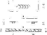
Figure 1A~Fig. 1 C is a manufacture method schematic diagram of having used the related semiconductor device of the 1st execution mode of the present invention.Present embodiment is used semiconductor chip 10 and wiring substrate 20.
The shape of semiconductor chip 10 can be cuboid (comprising cube), also can be spherical.Semiconductor chip 10 has a plurality of electrodes 12.Electrode 12 is outer electrodes of formed circuit element on semiconductor chip 10, is the not only flat but also thin dummy slider that forms with aluminium or copper etc.Electrode more than 12 is formed on any one side of semiconductor chip 10.Electrode 12 can be formed on the inboard that forms the service area of circuit element on the face of semiconductor chip 10, also can be formed at its outside.
Each electrode 12 is provided with flange 14.Flange 14 can be formed by one of them kind material such as gold, nickel, copper, silver, tin.The surface of flange 14 can be electroplated.Flange 14 can be electroplated by solder flux.The shape of flange 14 does not limit especially, can be pressed into flat, can form projection, or spherical good.The height of flange 14 does not limit especially.Flange 14 can be electroplated or electroless plating formation by electricity, also can form with the wire melting glomeration.Accompanying drawing example flange 14 is 1 segment structures, also can be different from this but multi-segment structure.
For example, wiring substrate 20 can adopt at liquid crystal polymer film BIAC (registered trade mark) and go up the soft copper paper tinsel overlapping board that forms Copper Foil (wiring 24).Like this, its water absorption rate is very low, even also can keep the high stability of its size under the environment of high humility.In addition, its thermal coefficient of expansion is set to and the roughly the same numerical value of Copper Foil (wiring 24), so can be owing to warpage takes place variations in temperature.
Shown in Figure 1A, semiconductor chip 10 is relative with basic substrate 20.As shown in the figure, when using a side surface to have the wiring substrate 20 of wiring 24, make the opposite side surface of wiring substrate 20 relative with semiconductor chip 10.The face that forms electrode 12 on the semiconductor chip 10 is towards wiring substrate 20.Semiconductor chip 10 adopts the so-called installation that faces down.
Each flange 14 of semiconductor chip 10 and each connecting portion 26 aligned position of wiring 24.Wiring substrate 20 is placed on the platform not shown in the figures, use fixedly semiconductor chip 10 aligned positions of anchor clamps 30.Anchor clamps 30 also can be adsorbed in semiconductor chip 10 formation fixed on the relative face of one side of electrode 12.Anchor clamps 30 inside have the heater 32 that carries out heat supply by thermal source in this illustrated example.
Next, shown in Figure 1B, the flange 14 with semiconductor chip 10 when making basic substrate 22 fusings is pressed in the basic substrate 22.In other words, when being pressed into basic substrate 22, the flange 14 with semiconductor chip 10 melts basic substrate 22 exactly.
Melting the energy that basic substrate 22 applied can be corresponding with the mechanical property that fusing takes place basic substrate 22.This energy can be radioactive ray (comprising visible light, ultraviolet ray, electron beam, X ray etc.) and heat energy etc.Example is to rely on heat energy to make basic substrate 20 fusings among the figure, at this moment can make its fusing by the basic substrate 22 of heater 32 heating of anchor clamps 30.Heater 32 will heat the flange 14 of semiconductor chip 10 at least.
For the flange 14 that is pressed into semiconductor chip 10, wherein direction the opposing party of semiconductor chip 10 or basic substrate 22 is pushed.For example, can make anchor clamps 30 be pressed against semiconductor chip 10 and push to basic substrate 22.As use anchor clamps 30, can melt basic substrate 22 and the flange 14 that is pressed into semiconductor chip 10 simultaneously.
Like this, shown in Fig. 1 C, flange 14 is embedded in the basic substrate 22 of fusing and forms with wiring 24 and is electrically connected.In view of the above, mechanically flange 14 is pressed into not melting basic substrate 22 and compares in the basic substrate 22, only flange 14 is formed with wiring 24 and be electrically connected with less pressure.In addition, owing to melted basic substrate 22, flange 14 can be pushed the molten material of basic substrate 22 and more positively arrive at connecting portion 26.
In addition, the face of semiconductor chip 10 can be combined closely with basic substrate 22.That is to say that semiconductor chip 10 can be pressed into basic substrate 22, the molten material of basic substrate 22 and the face of semiconductor chip 10 are combined closely.In this illustrated example, basic substrate 22 is combined closely and is formed the face of electrode 12 in semiconductor chip 10.In addition, the part of semiconductor chip 10 can be embedded in the basic substrate 22, also can not imbed.
In view of the above, semiconductor chip 10 and connecting up can form the state of the tight filling of material of the basic substrate 22 that is referred to etc. by tree between 26.Therefore, the stress that concentrates on each flange 14 (or connect up 24 each connecting portion 26) can be scattered on whole of semiconductor chip 10 by basic substrate 22.The stress that is subjected to of semiconductor chip 10 can be absorbed by basic substrate 22 in other words.
In addition, the thickness of basic substrate 22 can have the thickness of being given prominence on the face of electrode 12 greater than flange 14 from semiconductor chip 10.In view of the above, be convenient to make the part of semiconductor chip 10 to imbed in the basic substrate 22 and semiconductor chip 10 and basic substrate 22 are combined closely.
Describe with regard to the related semiconductor device of present embodiment below.But, omit in the following description with manufacture method in the record that repeats mutually of the description done.
Shown in Fig. 1 C, 1 comprises having plural electrode 12 and form the plural number wiring 24 wiring substrates 20 that constituted that have with the electrical connection section 26 of flange 14 at the semiconductor chip 10 that forms flange 14 on each electrode 12 and on basic substrate 22 in the semiconductor device.In this illustrated example, the one side of basic substrate 22 forms wiring 24.In other words, wiring substrate 20 has the face of basic substrate 22 sides and the face of wiring 24 sides.
In this illustrated example, semiconductor chip 10 is equipped on the face of basic substrate 22 sides of wiring substrate 20.And flange 14 is embedded in the basic substrate 22 and is electrically connected with wiring 24 formation.Flange 14 be positioned at basic substrate 22 on have an opposite side of face of semiconductor chip 10 the position be connected with connecting portion 26 formation.That is to say that flange 14 runs through basic substrate 22.Semiconductor chip 10 is installed in the wiring 24 in the so-called mode of facing down.
In view of the above, flange 14 and connecting portion 26 are sealed by basic substrate 22, thus different with wiring substrate 20, not necessarily need to fill the resin of sealing usefulness, thereby can reduce the number of spare parts of device.In addition, owing to flange 14 is embedded in the basic substrate 22, thereby can make semiconductor device become thinner.
The packing forms of the semiconductor device that present embodiment is related can be referred to as BGA (BallGrid Array) or CSP (Chip Size/Scale Package).And wiring substrate 20 can adopt COF (Chip On Flex/Film) to use plate with plate and COB (Chip On Board).
(the 2nd execution mode)
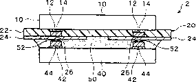
Fig. 2 and Fig. 3 are the schematic diagrames of having used the related semiconductor device of the 2nd execution mode of the present invention.Describe the mounting means of described semiconductor chip being applied to the example that multichip module forms resulting semiconductor device and manufacture method thereof in the present embodiment.And, can use the description of first execution mode in the following description as much as possible.
The 2nd semiconductor chip 40 is installed on by facing down on the face of wiring 24 sides of wiring substrate 20.As shown in Figure 2, the 2nd semiconductor chip 40 can be incorporated into by the anisotropic conductive material 50 that contains conducting particles 52 on the wiring substrate 20.At this moment, flange 44 forms with wiring 24 by conducting particles 52 and is electrically connected.
The 2nd semiconductor chip 40 can be and the 1st the corresponding mirror image chip of semiconductor chip.And each flange 44 can be connected in the position that forms the connecting portion 26 that is electrically connected with each flange 14 of first semiconductor chip 10.
In view of the above, for example when the 1st and the 2nd semiconductor chip 10,40 are memory, outside terminal (not shown) that can be by same arrangement carries out reading and writing of information on the memory cell of the identical address of memory separately.In addition, only select the connection of terminal just can separate the 1st and the 2nd semiconductor chip 10,40, can utilize the arrangement of same outside terminal to control at least two (can be most) semiconductor chips respectively in view of the above by chip.
In the related semiconductor device of present embodiment, the 2nd semiconductor chip 40 can be equipped on 24 formed of wirings, so semiconductor chip 10,40 can be installed on the two sides simply.And, because the flange 14 of the 1st semiconductor chip 10 is embedded in the basic substrate 22, so can make semiconductor device 2 become thinner.Therefore can provide cheaply and be small-sized multichip module.
Fig. 3 is the schematic diagram of the related manufacturing method for semiconductor device of present embodiment.The 1st and the 2nd semiconductor chip 10,40 can be equipped on respectively on the wiring substrate 20, also can roughly carry simultaneously.
When the 1st and the 2nd semiconductor chip 10,40 roughly are being both when carrying, can exert pressure from the both sides of 24 the connecting portion 26 of connecting up, so needn't be to 24 pressure that apply especially that connect up.And, carry simultaneously and can reduce the lift-launch time, thereby can enhance productivity.
When the 1st and the 2nd semiconductor chip 10,40 carry respectively, can carry the 1st semiconductor chip 10 earlier.Can after confirm that flange 14 is connected well with connecting portion 26, carry the 2nd semiconductor chip 40, thereby can reduce the generation of bad connection like this.
(the 3rd execution mode)
Fig. 4-Fig. 8 is a schematic diagram of having used the related semiconductor device of the 3rd execution mode of the present invention.The mounting means that the semiconductor chip that the 1st execution mode is set forth will be described in the present embodiment is applied to the resulting semiconductor device of multichip module form.And, can use the description in the described execution mode in the following description as far as possible.
(the 1st example)
Fig. 4 is the schematic diagram of the 1st example of the related semiconductor device of present embodiment.Semiconductor device 3 comprises the 1st and the 2nd semiconductor chip 10,60 and the substrate 20 that connects up.The difference of this 1st example and the example of the 2nd execution mode be the 1st and the 2nd semiconductor chip 10,6 (profile different.
The 2nd semiconductor chip 60 can greatly also can be littler than it than the profile of the 1st semiconductor chip 10.The connecting portion 28 of the position that connecting portion that the flange 64 on each electrode 62 is connected at the flange 14 with the 1st semiconductor chip 10 26 is different forms with wiring 24 and is electrically connected.
Omitted the outside terminal of wiring substrate 20 in this illustrated example.Outside terminal is connected in circuit block not shown in the figures (for example liquid crystal panel and master board).For example can extend the part of wiring substrate and manage to carry out the outside connection.That is to say, can be the lead-in wire of the some that is fixed on the wiring 24 on the basic substrate 22 as plug connector.
(the 2nd example)
Fig. 5 is the schematic diagram of the related semiconductor device of present embodiment the 2nd example.Semiconductor device 4 comprises that the 1st and the 10,70,2nd semiconductor chip 70 of the 2nd semiconductor chip are with resin 76 sealings.
The 2nd semiconductor chip 70 faces up and is installed on the wiring substrate 20.Electrode 72 is connected with connecting portion 28 by lead 74.Resin 76 can adopt the mold pressing resin that uses mould to make.In addition, also omitted the outside terminal of wiring substrate 20 in this illustrated example.
(the 3rd example)
Fig. 6 and Fig. 7 are the schematic diagram of the related semiconductor device of present embodiment the 3rd example.Semiconductor device 5 comprises the 1st and the 2nd semiconductor chip 10,40 and the substrate 20 that connects up.As outside terminal, on wiring substrate 20, be provided with the solder balls 80 of plural number.
In addition, with respect to the zone that solder balls 80 is set, the zone of carrying semiconductor chip can be made as more than two.Each zone of having carried semiconductor chip can be from plural direction convolution, thereby can produce the area of plane and the roughly the same semiconductor device of region area that solder balls 80 is set.
Solder balls 80 can protrude in basic substrate 22 sides of wiring substrate 20 as shown in the figure, also can protrude in wiring 22 sides of wiring substrate 20.When protruding in basic substrate 22 sides, solder balls 80 is outstanding by the through hole 23 of basic substrate 22.Through hole 23 is formed at and the 24 heavy mutually parts that connect up.It is to form by reflow process on the weld zone 25 that solder balls 80 can place preformed solder flux the part of wiring 24.
Solder balls perhaps is not set energetically, can forms to property solder balls 80 as a result by coating solder flux on circuit block.In addition, also can carry the semiconductor chip (not shown) in the setting area of solder balls 80.
Semiconductor device 6 shown in Figure 7 is formed by semiconductor device 5 bendings.Be that the setting area of zone that each semiconductor chip 10,40 is carried and solder balls 80 is overlapping and make this solder balls 80 outstanding laterally specifically.In view of the above, can provide small-sized and highdensity semiconductor device.
(the 4th example)
Fig. 8 is the schematic diagram of the related semiconductor device of present embodiment the 4th example.The part of the wiring 24 of semiconductor device 7 forms bend 90 and constitutes plural outside terminal.
Bend 90 is outstanding from the face of basic substrate 22.Be that wiring 24 forms bending at the front end position from basic substrate 22 projected directions specifically.The position at bend 90 places can form through hole 92 on the basic substrate 22.Like this, can make anchor clamps pass through hole 92 forms convex in wiring 24 bend 90 with convex position.
Among Fig. 8, bend 90 is side-prominent to the wiring 24 of wiring substrate 20, but also can be side-prominent to basic substrate 22 by through hole 92.Owing to utilize the part of wiring 24 to constitute outside terminal, so can reduce the number of spare parts of semiconductor device.
Bend 90 can make the central part projection in the part (for example weld zone) of wiring 24 and form.This moment, the inboard of bend 90 can the filling conductive paste etc.Because outside terminal is to utilize the wiring 24 (for example copper) harder than solder flux to form, thereby can improve the temperature cycle unfailing performance of device.
In addition, this example can be applied in described all execution modes with solder balls 80 to replace solder balls 80.
According to the form of described multichip module, because the 1st semiconductor chip 10 is equipped on basic substrate 22 sides of wiring substrate 20, so other semiconductor chips (the 2nd semiconductor chip 60,70) can be installed in every way simply in formation wiring 24 sides.And,, the flange 14 of semiconductor chip 10 can make the semiconductor device miniaturization that more becomes because being embedded in the basic substrate 22.Other effects are as being set forth in said embodiment.
Fig. 9 is a schematic diagram of having used the related circuit board of embodiments of the present invention.As shown in Figure 9, described semiconductor device forms with circuit board and is electrically connected.Circuit board can be a liquid crystal panel 100.Semiconductor device 1 is made shape that the basic substrate 22 of banded semiconductor device is become by the profile cut around plural number wiring 24.
As having the electronic equipment of having used semiconductor device of the present invention, Figure 10 illustrates notebook PC 200.Figure 11 illustrates mobile phone 300.This mobile phone 300 also has has used circuit board of the present invention (liquid crystal panel 100).
Claims (16)
1. the manufacture method of a semiconductor device is included in the operation of carrying semiconductor chip on the wiring substrate, and this wiring substrate forms wiring and constitutes on the basic substrate that is made of resiniferous material, wherein,
On the opposing face of the formation face that connects up described in the described basic substrate, the described basic substrate edge of fusing of marginization is pressed into the flange that is arranged on the described semiconductor chip described semiconductor-chip-mounting, and described flange is electrically connected with described wiring.
2. the manufacture method of the semiconductor device of claim 1 record, wherein,
Described wiring has the electrical connection section with described flange,
In described electrical connection operation, melt described basic substrate, with its material described flange and described connecting portion are sealed.
3. the manufacture method of the semiconductor device of claim 1 record, wherein,
In described electrical connection operation, melt described basic substrate, and the face of its material and described semiconductor chip is combined closely.
4. the manufacture method of the semiconductor device of claim 1 record, wherein,
In described electrical connection operation, by the described basic substrate of heat fused.
5. the manufacture method of the semiconductor device of claim 1 record, wherein,
Use thermoplastic resin as described basic substrate.
6. the manufacture method of the semiconductor device of claim 1 record, wherein,
In described electrical connection operation,, by heating the described flange that described anchor clamps heat described semiconductor chip at least, and described flange is imbedded in the described basic substrate by pressing described anchor clamps to described basic substrate with the fixing described semiconductor chip of anchor clamps.
7. claim 1 is to the manufacture method of the semiconductor device of one of claim 6 record, wherein,
Also be included in the operation of carrying other semiconductor chips on the described wiring substrate.
8. semiconductor device, it is made according to claim 1 to manufacture method of one of claim 6 record.
9. a semiconductor device comprises
Semiconductor chip has electrode, and forms flange on described electrode;
The wiring substrate forms the wiring that has with the electrical connection section of described flange on the basic substrate that is made of resiniferous material,
Described semiconductor-chip-mounting on the opposing face of the formation face that connects up described in the described basic substrate,
Described flange is imbedded described basic substrate and is electrically connected with described wiring,
Described flange and described connecting portion are by described basic substrate sealing.
10. the semiconductor device of claim 9 record, wherein,
The face of described basic substrate and described semiconductor chip is combined closely.
11. the semiconductor device of claim 9 record, wherein,
Described basic substrate is a thermoplastic resin.
12. the semiconductor device of claim 9 record, wherein,
Also comprise other semiconductor chips that are equipped on the described wiring substrate.
13. a circuit board, it has carried the semiconductor device of claim 8 record.
14. a circuit board, it has carried the semiconductor device of claim 9 to any record of claim 12.
15. an electronic equipment, it has the semiconductor device of claim 8 record.
16. an electronic equipment, it has the semiconductor device of claim 9 to any record of claim 12.
Applications Claiming Priority (3)
| Application Number | Priority Date | Filing Date | Title |
|---|---|---|---|
| JP2000395111A JP2002198395A (en) | 2000-12-26 | 2000-12-26 | Semiconductor device, its manufacturing method, circuit board, and electronic appliance |
| JP395111/2000 | 2000-12-26 | ||
| JP395111/00 | 2000-12-26 |
Publications (2)
| Publication Number | Publication Date |
|---|---|
| CN1362733A CN1362733A (en) | 2002-08-07 |
| CN1185698C true CN1185698C (en) | 2005-01-19 |
Family
ID=18860628
Family Applications (1)
| Application Number | Title | Priority Date | Filing Date |
|---|---|---|---|
| CNB011432926A Expired - Fee Related CN1185698C (en) | 2000-12-26 | 2001-12-26 | Semiconductor device and manufacture method thereof, circuit board and electronic apparatus |
Country Status (3)
| Country | Link |
|---|---|
| US (1) | US6846699B2 (en) |
| JP (1) | JP2002198395A (en) |
| CN (1) | CN1185698C (en) |
Families Citing this family (24)
| Publication number | Priority date | Publication date | Assignee | Title |
|---|---|---|---|---|
| SG122743A1 (en) * | 2001-08-21 | 2006-06-29 | Micron Technology Inc | Microelectronic devices and methods of manufacture |
| JP3914431B2 (en) * | 2001-12-26 | 2007-05-16 | 松下電器産業株式会社 | Manufacturing method of semiconductor device |
| US20030132528A1 (en) * | 2001-12-28 | 2003-07-17 | Jimmy Liang | Method and apparatus for flip chip device assembly by radiant heating |
| SG104293A1 (en) | 2002-01-09 | 2004-06-21 | Micron Technology Inc | Elimination of rdl using tape base flip chip on flex for die stacking |
| SG115455A1 (en) * | 2002-03-04 | 2005-10-28 | Micron Technology Inc | Methods for assembly and packaging of flip chip configured dice with interposer |
| SG115459A1 (en) * | 2002-03-04 | 2005-10-28 | Micron Technology Inc | Flip chip packaging using recessed interposer terminals |
| US6975035B2 (en) * | 2002-03-04 | 2005-12-13 | Micron Technology, Inc. | Method and apparatus for dielectric filling of flip chip on interposer assembly |
| SG121707A1 (en) * | 2002-03-04 | 2006-05-26 | Micron Technology Inc | Method and apparatus for flip-chip packaging providing testing capability |
| SG115456A1 (en) * | 2002-03-04 | 2005-10-28 | Micron Technology Inc | Semiconductor die packages with recessed interconnecting structures and methods for assembling the same |
| SG111935A1 (en) | 2002-03-04 | 2005-06-29 | Micron Technology Inc | Interposer configured to reduce the profiles of semiconductor device assemblies and packages including the same and methods |
| US6791168B1 (en) * | 2002-07-10 | 2004-09-14 | Micron Technology, Inc. | Semiconductor package with circuit side polymer layer and wafer level fabrication method |
| US20040036170A1 (en) * | 2002-08-20 | 2004-02-26 | Lee Teck Kheng | Double bumping of flexible substrate for first and second level interconnects |
| TW591780B (en) * | 2003-03-21 | 2004-06-11 | Univ Nat Central | Flip chip Au bump structure and method of manufacturing the same |
| DE10339609A1 (en) * | 2003-08-28 | 2005-03-24 | Forschungszentrum Karlsruhe Gmbh | Oligonucleotide, method and system for the detection of antibiotic resistance-mediating genes in microorganisms by means of real-time PCR |
| JP4593951B2 (en) * | 2004-03-29 | 2010-12-08 | ルネサスエレクトロニクス株式会社 | Multi-chip package manufacturing method |
| FR2875995B1 (en) * | 2004-09-24 | 2014-10-24 | Oberthur Card Syst Sa | METHOD FOR MOUNTING AN ELECTRONIC COMPONENT ON A SUPPORT, PREFERABLY MOU, AND ELECTRONIC ENTITY THUS OBTAINED, SUCH AS A PASSPORT |
| JP2006210566A (en) * | 2005-01-27 | 2006-08-10 | Akita Denshi Systems:Kk | Semiconductor device |
| JP4654865B2 (en) | 2005-09-30 | 2011-03-23 | パナソニック株式会社 | Electronic component mounting method |
| GB0705287D0 (en) * | 2007-03-20 | 2007-04-25 | Conductive Inkjet Tech Ltd | Electrical connection of components |
| JP4952353B2 (en) * | 2007-04-18 | 2012-06-13 | パナソニック株式会社 | Chip module and memory card |
| JP2011109046A (en) * | 2009-11-20 | 2011-06-02 | Sony Chemical & Information Device Corp | Mounting apparatus and method for manufacturing electronic module |
| US9252130B2 (en) * | 2013-03-29 | 2016-02-02 | Stats Chippac, Ltd. | Methods of manufacturing flip chip semiconductor packages using double-sided thermal compression bonding |
| US10147702B2 (en) * | 2016-10-24 | 2018-12-04 | Palo Alto Research Center Incorporated | Method for simultaneously bonding multiple chips of different heights on flexible substrates using anisotropic conductive film or paste |
| US20220230986A1 (en) * | 2021-01-18 | 2022-07-21 | Yibu Semiconductor Co., Ltd. | Semiconductor Assembly Packaging Method, Semiconductor Assembly and Electronic Device |
Family Cites Families (3)
| Publication number | Priority date | Publication date | Assignee | Title |
|---|---|---|---|---|
| JP3610999B2 (en) * | 1996-06-07 | 2005-01-19 | 松下電器産業株式会社 | Mounting method of semiconductor element |
| JPH10270496A (en) * | 1997-03-27 | 1998-10-09 | Hitachi Ltd | Electronic device, information processor, semiconductor device, semiconductor chip, and mounting method thereof |
| JP3654116B2 (en) * | 2000-03-10 | 2005-06-02 | セイコーエプソン株式会社 | Semiconductor device and manufacturing method thereof, circuit board, and electronic apparatus |
-
2000
- 2000-12-26 JP JP2000395111A patent/JP2002198395A/en not_active Withdrawn
-
2001
- 2001-11-14 US US09/987,409 patent/US6846699B2/en not_active Expired - Fee Related
- 2001-12-26 CN CNB011432926A patent/CN1185698C/en not_active Expired - Fee Related
Also Published As
| Publication number | Publication date |
|---|---|
| US6846699B2 (en) | 2005-01-25 |
| CN1362733A (en) | 2002-08-07 |
| JP2002198395A (en) | 2002-07-12 |
| US20020079594A1 (en) | 2002-06-27 |
Similar Documents
| Publication | Publication Date | Title |
|---|---|---|
| CN1185698C (en) | Semiconductor device and manufacture method thereof, circuit board and electronic apparatus | |
| CN1266766C (en) | Semiconductor device | |
| CN1143374C (en) | Semiconductor device, method of manufacture thereof, circuit board and electronic device | |
| CN1229863C (en) | Semiconductor device, method of manufacture thereof, circuit board, and electronic device | |
| CN1159956C (en) | Terminal electrode for circuit substrate on which chip pachage mounted and method for manufacturing the same | |
| CN1183485C (en) | Method for making chip card and the like | |
| CN1154178C (en) | Semiconductor device and method for manufacturing same, circuit substrate, and electronic device | |
| CN1291467C (en) | Electronic device and its manufacture method | |
| CN1110078C (en) | Method for mounting semiconductor chip | |
| CN1591861A (en) | Circuit component built-in module and method for manufacturing the same | |
| CN1532932A (en) | Semiconductor device and its producing method, electronic device and electronic instrument | |
| CN1575096A (en) | Electronic circuit device and its manufacturing method | |
| CN1452245A (en) | Semiconductor device and method for manufacturing the same | |
| CN1828880A (en) | Semiconductor device for fingerprint recognition | |
| CN1913144A (en) | Printed circuit board and electronic apparatus including printed circuit board | |
| CN1702857A (en) | Semiconductor device and method for manufacturing the same | |
| CN1672473A (en) | Method for manufacturing board with built-in device and board with built-in device, and method for manufacturing printed wiring board and printed wiring board | |
| CN1383197A (en) | Mfg. method of semiconductor device and semiconductor device | |
| CN1601713A (en) | Method of manufacturing semiconductor device | |
| CN1471178A (en) | Photoelectric element assembly | |
| CN1254856C (en) | Manufacturing method of circuit device | |
| CN1956177A (en) | Chip structure, chip package structure and its process | |
| CN1294652C (en) | Semiconductor device and its manufacturing method | |
| CN1542963A (en) | Semiconductor device and method of manufacturing the same, electronic device, electronic instrument | |
| WO2005027604A1 (en) | Method for mounting electronic component |
Legal Events
| Date | Code | Title | Description |
|---|---|---|---|
| C10 | Entry into substantive examination | ||
| SE01 | Entry into force of request for substantive examination | ||
| C06 | Publication | ||
| PB01 | Publication | ||
| C14 | Grant of patent or utility model | ||
| GR01 | Patent grant | ||
| C17 | Cessation of patent right | ||
| CF01 | Termination of patent right due to non-payment of annual fee |
Granted publication date: 20050119 Termination date: 20100126 |