CN1291467C - Electronic device and its manufacture method - Google Patents
Electronic device and its manufacture method Download PDFInfo
- Publication number
- CN1291467C CN1291467C CNB011252278A CN01125227A CN1291467C CN 1291467 C CN1291467 C CN 1291467C CN B011252278 A CNB011252278 A CN B011252278A CN 01125227 A CN01125227 A CN 01125227A CN 1291467 C CN1291467 C CN 1291467C
- Authority
- CN
- China
- Prior art keywords
- electronic component
- chip
- wiring plate
- solder paste
- paste material
- Prior art date
- Legal status (The legal status is an assumption and is not a legal conclusion. Google has not performed a legal analysis and makes no representation as to the accuracy of the status listed.)
- Expired - Fee Related
Links
Images


Classifications
-
- H—ELECTRICITY
- H05—ELECTRIC TECHNIQUES NOT OTHERWISE PROVIDED FOR
- H05K—PRINTED CIRCUITS; CASINGS OR CONSTRUCTIONAL DETAILS OF ELECTRIC APPARATUS; MANUFACTURE OF ASSEMBLAGES OF ELECTRICAL COMPONENTS
- H05K3/00—Apparatus or processes for manufacturing printed circuits
- H05K3/30—Assembling printed circuits with electric components, e.g. with resistor
- H05K3/32—Assembling printed circuits with electric components, e.g. with resistor electrically connecting electric components or wires to printed circuits
- H05K3/34—Assembling printed circuits with electric components, e.g. with resistor electrically connecting electric components or wires to printed circuits by soldering
- H05K3/341—Surface mounted components
-
- H—ELECTRICITY
- H01—ELECTRIC ELEMENTS
- H01L—SEMICONDUCTOR DEVICES NOT COVERED BY CLASS H10
- H01L21/00—Processes or apparatus adapted for the manufacture or treatment of semiconductor or solid state devices or of parts thereof
- H01L21/02—Manufacture or treatment of semiconductor devices or of parts thereof
- H01L21/04—Manufacture or treatment of semiconductor devices or of parts thereof the devices having at least one potential-jump barrier or surface barrier, e.g. PN junction, depletion layer or carrier concentration layer
- H01L21/50—Assembly of semiconductor devices using processes or apparatus not provided for in a single one of the subgroups H01L21/06 - H01L21/326, e.g. sealing of a cap to a base of a container
- H01L21/60—Attaching or detaching leads or other conductive members, to be used for carrying current to or from the device in operation
-
- H—ELECTRICITY
- H01—ELECTRIC ELEMENTS
- H01L—SEMICONDUCTOR DEVICES NOT COVERED BY CLASS H10
- H01L24/00—Arrangements for connecting or disconnecting semiconductor or solid-state bodies; Methods or apparatus related thereto
- H01L24/01—Means for bonding being attached to, or being formed on, the surface to be connected, e.g. chip-to-package, die-attach, "first-level" interconnects; Manufacturing methods related thereto
- H01L24/26—Layer connectors, e.g. plate connectors, solder or adhesive layers; Manufacturing methods related thereto
- H01L24/27—Manufacturing methods
-
- H—ELECTRICITY
- H01—ELECTRIC ELEMENTS
- H01L—SEMICONDUCTOR DEVICES NOT COVERED BY CLASS H10
- H01L2224/00—Indexing scheme for arrangements for connecting or disconnecting semiconductor or solid-state bodies and methods related thereto as covered by H01L24/00
- H01L2224/01—Means for bonding being attached to, or being formed on, the surface to be connected, e.g. chip-to-package, die-attach, "first-level" interconnects; Manufacturing methods related thereto
- H01L2224/26—Layer connectors, e.g. plate connectors, solder or adhesive layers; Manufacturing methods related thereto
- H01L2224/27—Manufacturing methods
- H01L2224/27001—Involving a temporary auxiliary member not forming part of the manufacturing apparatus, e.g. removable or sacrificial coating, film or substrate
-
- H—ELECTRICITY
- H01—ELECTRIC ELEMENTS
- H01L—SEMICONDUCTOR DEVICES NOT COVERED BY CLASS H10
- H01L2224/00—Indexing scheme for arrangements for connecting or disconnecting semiconductor or solid-state bodies and methods related thereto as covered by H01L24/00
- H01L2224/01—Means for bonding being attached to, or being formed on, the surface to be connected, e.g. chip-to-package, die-attach, "first-level" interconnects; Manufacturing methods related thereto
- H01L2224/42—Wire connectors; Manufacturing methods related thereto
- H01L2224/44—Structure, shape, material or disposition of the wire connectors prior to the connecting process
- H01L2224/45—Structure, shape, material or disposition of the wire connectors prior to the connecting process of an individual wire connector
- H01L2224/45001—Core members of the connector
- H01L2224/45099—Material
- H01L2224/451—Material with a principal constituent of the material being a metal or a metalloid, e.g. boron (B), silicon (Si), germanium (Ge), arsenic (As), antimony (Sb), tellurium (Te) and polonium (Po), and alloys thereof
- H01L2224/45138—Material with a principal constituent of the material being a metal or a metalloid, e.g. boron (B), silicon (Si), germanium (Ge), arsenic (As), antimony (Sb), tellurium (Te) and polonium (Po), and alloys thereof the principal constituent melting at a temperature of greater than or equal to 950°C and less than 1550°C
- H01L2224/45144—Gold (Au) as principal constituent
-
- H—ELECTRICITY
- H01—ELECTRIC ELEMENTS
- H01L—SEMICONDUCTOR DEVICES NOT COVERED BY CLASS H10
- H01L2224/00—Indexing scheme for arrangements for connecting or disconnecting semiconductor or solid-state bodies and methods related thereto as covered by H01L24/00
- H01L2224/73—Means for bonding being of different types provided for in two or more of groups H01L2224/10, H01L2224/18, H01L2224/26, H01L2224/34, H01L2224/42, H01L2224/50, H01L2224/63, H01L2224/71
- H01L2224/732—Location after the connecting process
- H01L2224/73201—Location after the connecting process on the same surface
- H01L2224/73203—Bump and layer connectors
- H01L2224/73204—Bump and layer connectors the bump connector being embedded into the layer connector
-
- H—ELECTRICITY
- H01—ELECTRIC ELEMENTS
- H01L—SEMICONDUCTOR DEVICES NOT COVERED BY CLASS H10
- H01L2224/00—Indexing scheme for arrangements for connecting or disconnecting semiconductor or solid-state bodies and methods related thereto as covered by H01L24/00
- H01L2224/80—Methods for connecting semiconductor or other solid state bodies using means for bonding being attached to, or being formed on, the surface to be connected
- H01L2224/83—Methods for connecting semiconductor or other solid state bodies using means for bonding being attached to, or being formed on, the surface to be connected using a layer connector
- H01L2224/8319—Arrangement of the layer connectors prior to mounting
- H01L2224/83192—Arrangement of the layer connectors prior to mounting wherein the layer connectors are disposed only on another item or body to be connected to the semiconductor or solid-state body
-
- H—ELECTRICITY
- H01—ELECTRIC ELEMENTS
- H01L—SEMICONDUCTOR DEVICES NOT COVERED BY CLASS H10
- H01L2924/00—Indexing scheme for arrangements or methods for connecting or disconnecting semiconductor or solid-state bodies as covered by H01L24/00
- H01L2924/10—Details of semiconductor or other solid state devices to be connected
- H01L2924/11—Device type
- H01L2924/14—Integrated circuits
-
- H—ELECTRICITY
- H01—ELECTRIC ELEMENTS
- H01L—SEMICONDUCTOR DEVICES NOT COVERED BY CLASS H10
- H01L2924/00—Indexing scheme for arrangements or methods for connecting or disconnecting semiconductor or solid-state bodies as covered by H01L24/00
- H01L2924/19—Details of hybrid assemblies other than the semiconductor or other solid state devices to be connected
- H01L2924/191—Disposition
- H01L2924/19101—Disposition of discrete passive components
- H01L2924/19105—Disposition of discrete passive components in a side-by-side arrangement on a common die mounting substrate
-
- H—ELECTRICITY
- H05—ELECTRIC TECHNIQUES NOT OTHERWISE PROVIDED FOR
- H05K—PRINTED CIRCUITS; CASINGS OR CONSTRUCTIONAL DETAILS OF ELECTRIC APPARATUS; MANUFACTURE OF ASSEMBLAGES OF ELECTRICAL COMPONENTS
- H05K2201/00—Indexing scheme relating to printed circuits covered by H05K1/00
- H05K2201/10—Details of components or other objects attached to or integrated in a printed circuit board
- H05K2201/10613—Details of electrical connections of non-printed components, e.g. special leads
- H05K2201/10621—Components characterised by their electrical contacts
- H05K2201/10636—Leadless chip, e.g. chip capacitor or resistor
-
- H—ELECTRICITY
- H05—ELECTRIC TECHNIQUES NOT OTHERWISE PROVIDED FOR
- H05K—PRINTED CIRCUITS; CASINGS OR CONSTRUCTIONAL DETAILS OF ELECTRIC APPARATUS; MANUFACTURE OF ASSEMBLAGES OF ELECTRICAL COMPONENTS
- H05K2201/00—Indexing scheme relating to printed circuits covered by H05K1/00
- H05K2201/10—Details of components or other objects attached to or integrated in a printed circuit board
- H05K2201/10613—Details of electrical connections of non-printed components, e.g. special leads
- H05K2201/10621—Components characterised by their electrical contacts
- H05K2201/10674—Flip chip
-
- H—ELECTRICITY
- H05—ELECTRIC TECHNIQUES NOT OTHERWISE PROVIDED FOR
- H05K—PRINTED CIRCUITS; CASINGS OR CONSTRUCTIONAL DETAILS OF ELECTRIC APPARATUS; MANUFACTURE OF ASSEMBLAGES OF ELECTRICAL COMPONENTS
- H05K2203/00—Indexing scheme relating to apparatus or processes for manufacturing printed circuits covered by H05K3/00
- H05K2203/02—Details related to mechanical or acoustic processing, e.g. drilling, punching, cutting, using ultrasound
- H05K2203/0278—Flat pressure, e.g. for connecting terminals with anisotropic conductive adhesive
-
- H—ELECTRICITY
- H05—ELECTRIC TECHNIQUES NOT OTHERWISE PROVIDED FOR
- H05K—PRINTED CIRCUITS; CASINGS OR CONSTRUCTIONAL DETAILS OF ELECTRIC APPARATUS; MANUFACTURE OF ASSEMBLAGES OF ELECTRICAL COMPONENTS
- H05K3/00—Apparatus or processes for manufacturing printed circuits
- H05K3/30—Assembling printed circuits with electric components, e.g. with resistor
- H05K3/32—Assembling printed circuits with electric components, e.g. with resistor electrically connecting electric components or wires to printed circuits
- H05K3/328—Assembling printed circuits with electric components, e.g. with resistor electrically connecting electric components or wires to printed circuits by welding
-
- Y—GENERAL TAGGING OF NEW TECHNOLOGICAL DEVELOPMENTS; GENERAL TAGGING OF CROSS-SECTIONAL TECHNOLOGIES SPANNING OVER SEVERAL SECTIONS OF THE IPC; TECHNICAL SUBJECTS COVERED BY FORMER USPC CROSS-REFERENCE ART COLLECTIONS [XRACs] AND DIGESTS
- Y02—TECHNOLOGIES OR APPLICATIONS FOR MITIGATION OR ADAPTATION AGAINST CLIMATE CHANGE
- Y02P—CLIMATE CHANGE MITIGATION TECHNOLOGIES IN THE PRODUCTION OR PROCESSING OF GOODS
- Y02P70/00—Climate change mitigation technologies in the production process for final industrial or consumer products
- Y02P70/50—Manufacturing or production processes characterised by the final manufactured product
-
- Y—GENERAL TAGGING OF NEW TECHNOLOGICAL DEVELOPMENTS; GENERAL TAGGING OF CROSS-SECTIONAL TECHNOLOGIES SPANNING OVER SEVERAL SECTIONS OF THE IPC; TECHNICAL SUBJECTS COVERED BY FORMER USPC CROSS-REFERENCE ART COLLECTIONS [XRACs] AND DIGESTS
- Y10—TECHNICAL SUBJECTS COVERED BY FORMER USPC
- Y10T—TECHNICAL SUBJECTS COVERED BY FORMER US CLASSIFICATION
- Y10T29/00—Metal working
- Y10T29/49—Method of mechanical manufacture
- Y10T29/49002—Electrical device making
- Y10T29/49117—Conductor or circuit manufacturing
- Y10T29/49124—On flat or curved insulated base, e.g., printed circuit, etc.
- Y10T29/49126—Assembling bases
-
- Y—GENERAL TAGGING OF NEW TECHNOLOGICAL DEVELOPMENTS; GENERAL TAGGING OF CROSS-SECTIONAL TECHNOLOGIES SPANNING OVER SEVERAL SECTIONS OF THE IPC; TECHNICAL SUBJECTS COVERED BY FORMER USPC CROSS-REFERENCE ART COLLECTIONS [XRACs] AND DIGESTS
- Y10—TECHNICAL SUBJECTS COVERED BY FORMER USPC
- Y10T—TECHNICAL SUBJECTS COVERED BY FORMER US CLASSIFICATION
- Y10T29/00—Metal working
- Y10T29/49—Method of mechanical manufacture
- Y10T29/49002—Electrical device making
- Y10T29/49117—Conductor or circuit manufacturing
- Y10T29/49124—On flat or curved insulated base, e.g., printed circuit, etc.
- Y10T29/4913—Assembling to base an electrical component, e.g., capacitor, etc.
- Y10T29/49131—Assembling to base an electrical component, e.g., capacitor, etc. by utilizing optical sighting device
-
- Y—GENERAL TAGGING OF NEW TECHNOLOGICAL DEVELOPMENTS; GENERAL TAGGING OF CROSS-SECTIONAL TECHNOLOGIES SPANNING OVER SEVERAL SECTIONS OF THE IPC; TECHNICAL SUBJECTS COVERED BY FORMER USPC CROSS-REFERENCE ART COLLECTIONS [XRACs] AND DIGESTS
- Y10—TECHNICAL SUBJECTS COVERED BY FORMER USPC
- Y10T—TECHNICAL SUBJECTS COVERED BY FORMER US CLASSIFICATION
- Y10T29/00—Metal working
- Y10T29/49—Method of mechanical manufacture
- Y10T29/49002—Electrical device making
- Y10T29/49117—Conductor or circuit manufacturing
- Y10T29/49124—On flat or curved insulated base, e.g., printed circuit, etc.
- Y10T29/4913—Assembling to base an electrical component, e.g., capacitor, etc.
- Y10T29/49133—Assembling to base an electrical component, e.g., capacitor, etc. with component orienting
- Y10T29/49137—Different components
-
- Y—GENERAL TAGGING OF NEW TECHNOLOGICAL DEVELOPMENTS; GENERAL TAGGING OF CROSS-SECTIONAL TECHNOLOGIES SPANNING OVER SEVERAL SECTIONS OF THE IPC; TECHNICAL SUBJECTS COVERED BY FORMER USPC CROSS-REFERENCE ART COLLECTIONS [XRACs] AND DIGESTS
- Y10—TECHNICAL SUBJECTS COVERED BY FORMER USPC
- Y10T—TECHNICAL SUBJECTS COVERED BY FORMER US CLASSIFICATION
- Y10T29/00—Metal working
- Y10T29/49—Method of mechanical manufacture
- Y10T29/49002—Electrical device making
- Y10T29/49117—Conductor or circuit manufacturing
- Y10T29/49124—On flat or curved insulated base, e.g., printed circuit, etc.
- Y10T29/4913—Assembling to base an electrical component, e.g., capacitor, etc.
- Y10T29/49139—Assembling to base an electrical component, e.g., capacitor, etc. by inserting component lead or terminal into base aperture
-
- Y—GENERAL TAGGING OF NEW TECHNOLOGICAL DEVELOPMENTS; GENERAL TAGGING OF CROSS-SECTIONAL TECHNOLOGIES SPANNING OVER SEVERAL SECTIONS OF THE IPC; TECHNICAL SUBJECTS COVERED BY FORMER USPC CROSS-REFERENCE ART COLLECTIONS [XRACs] AND DIGESTS
- Y10—TECHNICAL SUBJECTS COVERED BY FORMER USPC
- Y10T—TECHNICAL SUBJECTS COVERED BY FORMER US CLASSIFICATION
- Y10T29/00—Metal working
- Y10T29/49—Method of mechanical manufacture
- Y10T29/49002—Electrical device making
- Y10T29/49117—Conductor or circuit manufacturing
- Y10T29/49124—On flat or curved insulated base, e.g., printed circuit, etc.
- Y10T29/4913—Assembling to base an electrical component, e.g., capacitor, etc.
- Y10T29/49144—Assembling to base an electrical component, e.g., capacitor, etc. by metal fusion
-
- Y—GENERAL TAGGING OF NEW TECHNOLOGICAL DEVELOPMENTS; GENERAL TAGGING OF CROSS-SECTIONAL TECHNOLOGIES SPANNING OVER SEVERAL SECTIONS OF THE IPC; TECHNICAL SUBJECTS COVERED BY FORMER USPC CROSS-REFERENCE ART COLLECTIONS [XRACs] AND DIGESTS
- Y10—TECHNICAL SUBJECTS COVERED BY FORMER USPC
- Y10T—TECHNICAL SUBJECTS COVERED BY FORMER US CLASSIFICATION
- Y10T29/00—Metal working
- Y10T29/49—Method of mechanical manufacture
- Y10T29/49002—Electrical device making
- Y10T29/49117—Conductor or circuit manufacturing
- Y10T29/49124—On flat or curved insulated base, e.g., printed circuit, etc.
- Y10T29/49147—Assembling terminal to base
- Y10T29/49149—Assembling terminal to base by metal fusion bonding
Abstract
A method of manufacturing an electronic device including a first electronic component mounted on one main surface of a wiring board by being thermo-compression bonded by means of a thermo-compression bonding tool with an adhesive resin interposed between a first area of the one main surface of the wiring board and the first electronic component, and a second electronic component mounted on a second area different from the first area of the one main surface of the wiring board by melting a soldering paste material and higher than the first electronic component in post-mounting height, and wherein the first electronic component is mounted before the mounting of the second electronic component.
Description
Technical field
The present invention relates to a kind of electronic device and manufacture method thereof, particularly a kind of technology that can effectively be applied on wiring plate, to be equipped with the electronic device of electronic component, this technology is applicable to different execution modes.
Background technology
Everybody is used as electronic device with the electronic device of so-called " MCM (multi-chip module) " now.MCM is the device that a kind of integrated functionality of formation on the wiring plate was installed or be implemented in to a kind of a plurality of semiconductor chip, all is formed with integrated circuit in said each semiconductor chip.In order to accelerate the message transmission rate of MCM, and reduce its size, effectively the flip-chip mounting technique is used for MCM, according to this technology, form on the lip-deep electrode pad being arranged at circuit respectively, form projected electrode, and it is installed on the wiring plate.
In the flip-chip mounting technique, proposed various installations or method for packing or system, and dropped into practical application.One of them is that the ACF that utilizes the sheet anisotropic conductive film to make binder resin installs or package system (ACF: anisotropic conductive film).The ACF installation system is a kind of method that is applied to semiconductor chip, wherein, be arranged at circuit form the surface electrode pad on, for example each all comprises the binding post salient point of gold (Au) in formation respectively, at the ACF resin clip under the state between semiconductor chip and the wiring plate, the thermocompression bonding semiconductor chip with semiconductor chip welding and be fixed on the wiring plate, and is electrically connected the coupling part of connecting up on the wiring plate and the electrode pad of semiconductor chip respectively.Anisotropic conductive film is by mixing the conducting film that a large amount of conductive particles obtain with discrete form in the dielectric film resin.Do not introduced this ACF mounting technique in openly flat 10 (1998)-270496 (USP.6,208,525) of unexamined patent.
Non-conductive film), utilize the paste-like anisotropic conductive resin to make the ACP installation system of binder resin (ACP: anisotropic conductive cream) etc. except that the ACF installation system, utilize the sheet non-conductive film to make the NCF installation system of binder resin (NCF: in addition.
On the other hand, except that semiconductor chip, by welded and installed or be encapsulated in welding device on the wiring plate or surperficial installing device (SMD: surface mounted device) is made in the electronic component common name.Soldering of electronic components comprises passive component or parts and active element or parts.As the welding passive component, chip capacitor, chip resistor, chip inductor etc. are for example arranged.About the welding active element, for example have such as BGA (ball grid array) type, CSP (chip size packages) type, QFP (quad-flat-pack) type, QFN (quad flat no-leads encapsulation) type etc. all to comprise the semiconductor device of the semiconductor chip that has encapsulated.
Summary of the invention
Meanwhile, the inventor has developed a kind of MCM, wherein in the ACG installation system, utilize thermocompression bonding mounted semiconductor chip (after this being called " IC (integrated circuit) chip is installed in pressure welding ") and soldering of electronic components, be arranged on the same wiring plate by hybrid mode.When this MCM of exploitation, the inventor has found following problem.
(1) soldering of electronic components comprises that some install back height (corresponding to the height from the main surface of wiring plate to its top) and be higher than the element that the IC chip is installed in pressure welding.During setting height(from bottom) is big before in pressure welding the IC chip being installed these soldering of electronic components, install in the IC chip processes in that pressure welding is installed, the hot pressing soldering tip of IC chip is installed in the thermocompression bonding pressure welding, contacts mounted soldering of electronic components easily.Therefore, need widen the interval that the IC chip chamber is installed in its corresponding pressure welding of each soldering of electronic components.In addition, so also can hinder reducing of MCM size.
When from improving the generation rate angle, when wishing that the IC chip is installed in a plurality of pressure weldings of thermocompression bonding together,, need the pressure-welding head that uses the IC chip is installed greater than pressure welding for thermal head.Yet, when in hot pressing soldering tip scope, having highly big soldering of electronic components, be difficult to these IC chips of thermocompression bonding together.
(2) on the coupling part of the wiring on the wiring plate, apply solder paste material (corresponding to semisolid welding material) by a large amount of solder grains are mixed with solder flux and knead and obtain together, then, soldering of electronic components is installed, the coupling part of the wiring on the wiring plate and the respective electrode of soldering of electronic components are partly faced, thereby the solder paste material that makes them and be clipped between them is faced, and then, they is heat-treated, the fusing solder paste material carries out the installation of soldering of electronic components thus.Apply solder paste material, adopt silk screen print method or dispersion method.Silk screen print method is a kind of scraper plate that utilizes, and each hole or the opening of solder paste material by limiting on screen mask with being arranged on the screen mask is delivered to the method on the substrate surface.Dispersion method is a kind ofly by thin nozzle solder paste material to be discharged, and the method for coating.
The silk screen print method that can apply solder paste material together is applicable to the productivity ratio that improves MCM.Yet,, when pressure welding installation IC chip is installed, is difficult in when soldering of electronic components is installed and utilizes silk screen printing to apply solder paste material when before each soldering of electronic components.By adopting so-called " the convex-concave mask " that has a jut at the part place that the IC chip is installed in mounted pressure welding at least, carry out applying of solder paste material, avoiding this part, thereby allow to apply solder paste material by once-through operation.Yet, in this case, need set the planar dimension of the jut of convex-concave mask to such an extent that the planar dimension of IC chip is installed, thereby produce level and smooth shape for lugs greater than pressure welding, scraper plate can successfully be slipped over.Therefore, soldering of electronic components can not be arranged on pressure welding and install near the electronic component, thereby has hindered reducing of MCM size.
(3) to select radiator for the high MCM that dissipates of needs.Expose owing to form the back side of the relative pressure welding installation IC chip in surface with its circuit, radiator is installed on the back side of pressure welding installation IC chip by the conducting strip that is clipped in therebetween, and the IC chip is installed in pressure welding can have good radiation effect.Yet when highly being higher than pressure welding the soldering of electronic components of IC chip being installed being existed after installing, these soldering of electronic components can hinder pressure welding that contacting between IC chip and conducting strip is installed, and have therefore reduced the dissipation of MCM.
The object of the present invention is to provide a kind of technology that can improve electronic device productivity ratio.
Another purpose of the present invention is to provide a kind of technology that can reduce the size of electronic device.
Still a further object of the present invention provides a kind of technology that can improve the dissipation of electronic device.
Above and other objects of the present invention and novel feature will become clearer by introduction and each accompanying drawing of this specification.
Briefly introduce the overview of disclosed every invention among the application below:
(1) provides a kind of method of making electronic device, said electronic device comprises: first electronic component, first electronic component is to utilize first district of a first type surface that is clipped in wiring plate and the binder resin between first electronic component, utilize the hot pressing soldering tip, by thermocompression bonding, of being installed in wiring plate is lip-deep; Second electronic component, second electronic component is by the fusing solder paste material, is installed in second district that is different from first district of a said first type surface of wiring plate, and the height after its installation is higher than first electronic component, wherein before second electronic component is installed, first electronic component is installed.
(2) in the said method of above-mentioned (1) bar, binder resin is a thermosetting resin.
(3) in the said method of above-mentioned (1) bar, during thermocompression bonding first electronic component, the temperature of hot pressing soldering tip is higher than the fusing point of solder paste material.
(4) in the said method of above-mentioned (1) bar, first electronic component is the active parts that wherein is formed with circuit, and second electronic component is a passive component.
(5) provide a kind of method of making electronic device, said electronic device comprises: first electronic component, said first electronic component is to utilize first district of a first type surface that is clipped in wiring plate and the binder resin between said first electronic component, utilize the hot pressing soldering tip, be installed to by thermocompression bonding on the first type surface of wiring plate; Second electronic component, second electronic component are by the fusing solder paste material, are installed in second district that is different from first district of a first type surface of wiring plate, wherein before installation first electronic component, second electronic component are installed.
(6) in the said method of above-mentioned (5) bar, utilize silk screen print method to carry out applying of solder paste material.
(7) in the said method of above-mentioned (5) bar, highly be higher than said first electronic component after the installation of second electronic component.
(8) in the said method of above-mentioned (5) bar, first electronic component is the passive component that wherein is formed with circuit, and second electronic component is an active parts.
(9) provide a kind of electronic device, comprising:
Wiring plate;
Be implemented in a plurality of first electronic components in first district of a first type surface of wiring plate;
Be implemented in a plurality of second electronic components in second district that is different from first district of a said first type surface of wiring plate, each second electronic component tool extends to the height on top from a said first type surface of wiring plate, and this highly is higher than the height of each first electronic component; And
Be installed on a plurality of first electronic components, and be not installed to conducting strip on a plurality of second electronic components.
(10) in the said electronic device of above-mentioned (9) bar, provide the radiator that is installed on the said conducting strip, the planar dimension of this radiator forms and covers a plurality of first electronic components and a plurality of second electronic component.
Description of drawings
Although this specification finishes with the claim as theme of the present invention that particularly points out and explicitly call for, but believe, by the introduction of doing below in conjunction with accompanying drawing, the present invention may be better understood, purpose of the present invention and feature and other purpose, feature and advantage, wherein:
Fig. 1 is a plane graph of showing the MCM (electronic device) of first embodiment of the invention;
Fig. 2 is the bottom view of MCM shown in Figure 1;
Fig. 3 is a profile of showing the installment state that builds on control chip, buffer chip and chip capacitor among the MCM shown in Figure 1;
Fig. 4 (A) and 4 (B) are the profiles of manufacture method of describing the MCM of first embodiment of the invention;
Fig. 5 (A) and 5 (B) are the profiles of manufacture method of describing the MCM of first embodiment of the invention;
Fig. 6 (A) and 6 (B) are the profiles of manufacture method of describing the MCM of first embodiment of the invention;
Fig. 7 (A) and 7 (B) are the profiles of manufacture method of describing the MCM of first embodiment of the invention;
Fig. 8 is a plane graph of describing the manufacture method of first embodiment of the present invention MCM;
Fig. 9 is a plane graph of describing the manufacture method of first embodiment of the present invention MCM;
Figure 10 (A) and 10 (B) are the profiles of manufacture method of describing the MCM of second embodiment of the invention;
Figure 11 (A) and 11 (B) are the profiles of manufacture method of describing the MCM of second embodiment of the invention;
Figure 12 (A) and 12 (B) are the profiles of manufacture method of describing the MCM of second embodiment of the invention;
Figure 13 (A) and 13 (B) are the profiles of manufacture method of describing the MCM of second embodiment of the invention;
Figure 14 (A) and 14 (B) are the profiles of manufacture method of describing the MCM of second embodiment of the invention;
Figure 15 is the profile of manufacture method of describing the MCM of second embodiment of the invention;
Figure 16 is the plane graph of manufacture method of describing the MCM of second embodiment of the invention;
Figure 17 is the plane graph of manufacture method of describing the MCM of second embodiment of the invention;
Figure 18 is the profile of schematic construction of showing the illustration MCM of third embodiment of the invention;
Figure 19 is the design drawing of MCM shown in Figure 180;
Figure 20 is the design drawing of MCM shown in Figure 180;
Figure 21 is the profile that the present invention can't be applied to MCM wherein.
Embodiment
Introduce the preferred embodiments of the present invention in detail below in conjunction with accompanying drawing.
Incidentally, in introducing each accompanying drawing of various embodiments of the present invention, have the parts of same function, represent by identical reference number respectively, therefore will omit the introduction that repeats them.
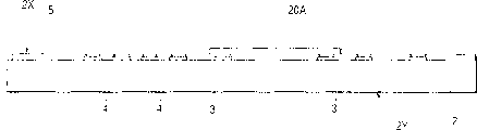
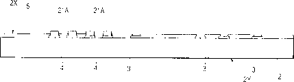
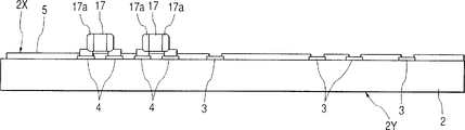
Fig. 1 is a plane graph of showing the MCM (electronic device) of first embodiment of the invention.Fig. 2 is the bottom view of MCM shown in Figure 1; Fig. 3 is a profile of showing the installment state that builds on control chip, buffer chip and chip capacitor among the MCM shown in Figure 1.Incidentally, omitted the hatching of section among Fig. 3, so that observe accompanying drawing.
As illustrated in fig. 1 and 2, structure according to the MCM (electronic device) 1 of present embodiment is as follows, a plurality of welding assemblies or element and crimping IC chip are arranged on the first type surface 2X of wiring plate 2, a plurality of spherical solder salient points 22 are arranged on reverse side opposite with the first type surface 2X of wiring plate 2 or dorsal part (another first type surface) 2Y, as external connection terminals.Wherein be formed with control circuit a semiconductor chip (after this claim " control chip ") 10, each all is formed with memory circuit (for example, SDRAM: four semiconductor chips (after this being called " storage chip ") 12 Synchronous Dynamic Random Access Memory), five semiconductor chips (after this being called " buffer chip ") 14 that each all is formed with buffer circuit and the semiconductor chip 16 that wherein is formed with the NAND circuit is as crimping IC chip.Electronic unit is installed in these pressure weldings or element is installed or encapsulation by the ACF package system.A plurality of chip capacitors (17,18) and chip resistor 19 are as welding electronic unit or element.These soldering of electronic components are installed by the Reflow Soldering method.
Solder bump 22 is for example formed by the scolder with Pb-Sn composition respectively.Respective electrode pad electricity and mechanical connection on solder bump 22 and the back side 2Y that is arranged at wiring plate 2.
The flat shape of control chip 10, storage chip 12, buffer chip 14 and compute chip 16 forms square respectively.In the present embodiment, buffer chip 14 and storage chip 12 for example form rectangle respectively, and that control chip 10 and compute chip 16 for example form respectively is square.
Although to control chip 10, storage chip 12, buffer chip 14 and compute chip 16 without limits, they constitute respectively and should have Semiconductor substrate, form the multilayer interconnection layer that repeatedly stacked insulating barrier and wiring layer form on the surface and form the surface protection film (final protection) that covers the multilayer interconnection layer by the circuit in Semiconductor substrate in principle.Semiconductor substrate is for example formed by monocrystalline silicon, and insulating barrier is for example formed by silicon oxide film, and wiring layer is formed by metal films such as for example aluminium (Al) or aluminium alloys.The surface protection film of each storage chip 12 is for example formed by the polyimide resin of the anti-alpha ray intensity that can improve memory.The surface protection film of each in control chip 10, buffer chip 14 and the compute chip 16 is all formed by for example dielectric film such as silica or silicon nitride.
Although do not specifically illustrate, wiring plate 2 constitute have rigid substrates, (build-up process) is formed at the flexible layer on the rigid substrates and is formed at dielectric film 5 on the flexible layer to utilize build-up process.Rigid substrates and flexible layer form multilayer interconnect structure.Each insulating barrier of rigid substrates for example all is made of the elastomeric resin plate that utilizes epoxy resin or polyimide resin-impregnated glass fibre to obtain.Each insulating barrier that is used for flexible layer is all formed by low elasticity epoxy resin.In addition, each wiring layer of rigid substrates and flexible layer are formed by the metal film that for example comprises copper (Cu) respectively.Dielectric film 5 is for example formed by epoxy resin.Dielectric film 5 is used for control when installing, and scolder leaks spreads to soldering of electronic components (present embodiment is 17,18 and 19) on, (be 10,12 in the present embodiment with regard to pressure welding installation electronic unit or element, 14 and 16), be used for guaranteeing the bonding force of the bonding or welding resin that encapsulates.
A plurality of coupling parts 3 and electrode pad 4 are provided in wiring layer, and they all are included in the wiring portion corresponding to the upper strata of wiring plate 2 that forms in the wiring layer.These coupling parts 3 and electrode pad 4 be respectively by being defined in hole or the opening in the dielectric film 5, exposes from a first type surface 2X of wiring plate 2.
As shown in Figure 3, in control chip 10 and each buffer chip 14, a plurality of electrode pads (10a and 14a) are formed at a first type surface corresponding respectively to each chip and the corresponding circuits of another first type surface on the other side forms surface (10X and 14X).A plurality of electrode pads of each chip (10a and 14a) are formed in the corresponding wiring line layer corresponding to the upper strata of the multilayer interconnection layer of each chip.Their bonding opening or holes by limiting in the surface protection film of each chip form the surface from the corresponding circuits of each chip and expose.Although not shown, be similar to control chip 10 and the mode that cushions chip 14, even under the situation of two chips, the related circuit that a plurality of electrode pads also can be formed at memory and compute chip 12 and 16 forms on the surface.The electrode pad 14a of the electrode pad 10a of control chip 10 and buffering chip 14 and the electrode pad of compute chip 16 all are provided with by the mode that four face down bonding dishes are arranged, and the electrode pad of each storage chip 12 all is provided with by the mode that center bonding pads is arranged.
Stage before mounting process, for example the binding post salient point 11 that constitutes by Au be formed on the electrode pad of control chip 10 and buffering chip 14 respectively and on the electrode pad of storage chip 12 and compute chip 16 as projected electrode.Binding post salient point 11 for example utilizes as the Au silk etc., and forms in conjunction with the ball bonding method of ultrasonic vibration and thermocompression bonding.This ball bonding method is a kind of like this method, and at first the exit at the Au silk forms ball, when applying ultrasonic vibration thereon then, these ball thermocompression bondings are received on the respective electrode pad of each chip, then, cut off the Au silk, thereby form salient point from each ball portion.So the binding post salient point that is formed on the electrode pad is firmly attached on the corresponding electrode pad.
As shown in Figure 3, form under the state of surperficial 10X in the face of a first type surface 2X of wiring plate 2 installation and control chip 10 at its circuit.For example, sandwich anisotropic conductive resin 20 at each buffer chip 14 and 2 of wiring plates, as bonding or binder resin.Control chip 10 by anisotropic conductive resin 20 bondings and be fixed to the wiring fabric swatch 2 on.
The binding post salient point 11 of control chip 10 is separately positioned between each electrode pad 10a and each coupling part 3 on the wiring plate 2 of control chip 10, thereby is electrically connected both by being defined in the opening in the dielectric film 5.Utilization is clipped in the thermal shrinkage force (being equivalent to the convergent force that anisotropic conductive resin 20 produces when being heated recovering state to room temperature state) of the anisotropic conductive resin 20 of 10 of wiring plate 2 and control chips, hot curing convergent force (be equivalent to produce when thermosetting resin cured convergent force), the crimp forces that the hot pressing soldering tip produces etc. are bonded to binding post salient point 11 on the corresponding coupling part 5a of wiring plate 2.The partially conductive particle that is mixed in a large number in the anisotropic conductive resin 20 is clipped in respectively between the coupling part 5a of binding post salient point 11 and wiring plate 2.Incidentally, storage chip 12, buffer chip 14 and compute chip 16 also encapsulate or install by the mode that is similar to control chip 10.
Each chip capacitor 17 forms rectangle, has electrode part 17a at their two ends.Chip capacitor 18 and plate resistor 19 also constitute by the mode that is similar to chip capacitor 17. Chip capacitor 17 and 18 and chip resistor 19 by being limited to the opening in the dielectric film 5, by scolder 21 electricity be mechanically connected on the respective electrode pad 4 of wiring plate 2.
The height (being equivalent to the height from a first type surface 2X of wiring plate 2 to the top that the back electronic component is installed) that each electronic component of back is installed is as follows.
The height of control chip 10 and storage chip 12 is about 0.4mm, the height of buffer chip 14 and compute chip 16 is about 0.28mm, the height of each chip capacitor 17 is about 0.85mm, and the height of each chip capacitor 18 is about 0.8mm, and the height of each chip resistor 19 is about 0.45mm.
Introduce the manufacture method of MCM 1 below in conjunction with Fig. 4 to 9.Fig. 4 to 7 is respectively a profile of describing the manufacturing process of MCM, and Fig. 8 and 9 is respectively a plane graph of describing the manufacturing process of MCM.Incidentally, omitted the hatching of section among Fig. 4-7, so that observe accompanying drawing.
About present embodiment, after being presented in pressure welding below the installation or encapsulation of electronic component being installed, the embodiment of soldering of electronic components is installed.
At first prepare pressure welding installation electronic component (corresponding to control chip 10, storage chip 12, buffer chip 14 and computing or arithmetic chip 16) and soldering of electronic components (corresponding to chip capacitor 17 and 18, and the wiring plate 2 shown in preparation Fig. 4 (A) chip resistor 19).Binding post pad 11 has been formed on the respective electrode pad of control chip 10, storage chip 12, buffer chip 14 and compute chip 16.
Then, shown in Fig. 4 (B), utilize coating or adhesion instrument (adhering to head) 25, with sheet anisotropic conductive resin film 20A from the corresponding control chip that applies band (cover tape) 23 and transfer to a first type surface of wiring plate 2 install or loading area on.Shown in Fig. 5 (A), anisotropic conductive resin film 20A is arranged on the corresponding control chip installing zone of a first type surface 2X of wiring plate 2.Can adopt and for example a large amount of conductive particles are mixed in the anisotropic conductive resin film 20A that thermosetting epoxy resin obtains.
Then, shown in Fig. 5 (B), control corresponding chip 10 is arranged on the corresponding control chip installing zone of a first type surface 2X of wiring plate 2, accompanies anisotropic conductive resin film 20A between the two.Control chip 10 is arranged to its circuit and is formed the first type surface 2X of surperficial 10X in the face of wiring plate 2.Utilize the chuck that transports of chip loader, control chip 10 is delivered to the control chip installing zone of a first type surface 2X of wiring plate 2 from memory disc.
Then, shown in Fig. 6 (A), utilize hot pressing soldering tip 26A, thermocompression bonding control chip 10, thereby the corresponding coupling part 3 of connection binding post salient point 11 and wiring plate 2.Then, keep its thermocompression bonding state to solidify up to anisotropic conductive resin film 20A.Anisotropic conductive resin film 20A fusing is once solidified then.So shown in Fig. 6 (B), control chip 10 is bonding and be fixed on the wiring plate 2 by the anisotropic conductive resin that solidifies 20.The electrode pad 10a of control chip 10 is bonded on the corresponding coupling part 3 of wiring plate 2, thereby by binding post salient point 11 be mixed into partially conductive particle in the anisotropic conductive resin 20 in a large number, is electrically connected to the coupling part 3 of wiring plate 2.By this technology, the teflon sheet 24 that the thermocompression bonding utilization of chip is clipped between control chip 10 and the hot pressing soldering tip 26A is carried out.
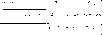
Then, utilize the method that is similar to control chip 10, each storage chip 12 is arranged on the respective stored chip installation area of a first type surface 2X of wiring plate 2.Then, utilize the method that is similar to control chip 10, each buffer chip 14 is arranged on the corresponding buffer chip installing zone of a first type surface 2X of wiring plate 2.Afterwards, utilize the method that is similar to control chip 10, each compute chip 16 is arranged on the corresponding compute chip installing zone of a first type surface 2X of wiring plate 2.So as shown in Figure 8, the element that pressure welding is installed or encapsulated is arranged on the first type surface 2X of wiring plate 2.
Before the installation of electronic component being installed in pressure welding, install when soldering of electronic components highly big after the electronic package being installed than pressure welding, be used for the thermocompression bonding pressure welding hot pressing soldering tip 26A of the electronic component mounted soldered elements of contact easily that becomes is installed.Therefore, need widen each soldered elements and corresponding pressure welding interval between electronic component is installed.Yet, as present embodiment, before soldering of electronic components, pressure welding is installed electronic component is installed, can eliminate the problem of hot pressing soldering tip 26A contact soldered elements substantially.Therefore, the interval that soldering of electronic components and corresponding pressure welding are installed between electronic component narrows down.
In addition, in the present embodiment, under the condition of 180 ℃ and 20 seconds, carry out the curing of anisotropic conductive resin film 20A.After in advance the temperature of wiring plate 2 being set to 65 ℃, utilize the hot pressing soldering tip 26A that is heated to 235 ℃, carry out the heating of this moment.When comparing with these thermocompression bonding process conditions, under the condition of 200 ℃ and 10 seconds, solidify anisotropic conductive resin film 20A, when further boosting productivity, the design temperature of hot pressing soldering tip 26A need be provided to 265 ℃, the temperature of wiring plate 2 remains on 65 ℃ simultaneously.
When the treatment temperature of thermocompression bonding technology as the fusing point of the scolder of solder paste material 21A (for example is higher than, 183 ℃) time, if before electronic component is installed in pressure welding, soldering of electronic components is installed, the scolder of each soldered elements can be owing to the heat during the thermocompression bonding technology melts.When tool not adopts its size can cover the hot pressing soldering tip 26A of installing zone of soldering of electronic components, even under the situation of height after the installation that highly is higher or lower than each pressure welding installation electronic component after the installation of each soldering of electronic components, scolder also can melt, therefore, can cause the problem of for example omitting each soldering of electronic components.Yet, when as present embodiment, pressure welding is installed when electronic component is installed before soldering of electronic components, the heat treatment during the thermocompression bonding technology does not produce dysgenic danger to soldering of electronic components.In addition, the heat during the technology of fusing solder paste material 21A also almost is being safe from danger aspect the anisotropic conductive resin 20 generation harmful effects of having solidified.So, useful effect is because before soldering of electronic components, pressure welding is installed electronic component is installed, even can be used for the big hot pressing soldering tip 26A of thermocompression bonding large chip, and the technology of a plurality of chips of thermocompression bonding also can be used for the technology of the little chip of thermocompression bonding together.
When electronic component is installed in a plurality of pressure weldings of hope thermocompression bonding together, when boosting productivity, need to adopt the hot pressing soldering tip that electronic component is installed greater than pressure welding.If in this case, the soldering of electronic components of big height is present in the pressure-welding head scope, be difficult to thermocompression bonding together they.Yet, pressure welding was installed before soldering of electronic components electronic component is installed, electronic component is installed in a plurality of pressure weldings of thermocompression bonding together.
When what introduce as present embodiment, adopt when greater than pressure welding the hot pressing soldering tip 26A of electronic component being installed at least, teflon sheet 24 can be clipped in each pressure welding and install between electronic component and the hot pressing soldering tip 26A, and is contaminated owing to the anisotropic conductive resin 20 of the periphery extension that electronic component is installed towards each pressure welding to prevent a thermocompression bonding 26A.
Then, on a first type surface 2X of wiring plate 2, on each electrode pad 4, apply solder paste material 21A.Utilize dispersion method to carry out applying of solder paste material 21A, solder paste material 21A is discharged from thin nozzle 27, put on each electrode pad, shown in Fig. 7 (A).About solder paste material 21A, can adopt and mix at least and solder paste material that knead thin solder grain and solder flux obtain.In the present embodiment, for example, can adopt and mix and the composition of kneading is the solder paste material that the solder grain of 37wt%Pb-63wt%Sn obtains.Incidentally, solder flux can comprise rosin, active material and organic solvent etc.
Then, shown in Fig. 7 (B), on the respective electrode pad 4 of a first type surface 2X of wiring plate 2, chip capacitor 17 and 18 and chip resistor 19 are set, accompany solder paste material 21A between the two.Afterwards, heat-treat, with fusing solder paste material 21A, thereby as shown in Figure 3, the electrode pad 4 on the wiring plate 2 and the electrode 17A of chip capacitor 17 pass through scolder 21 electricity and mechanical connection each other, the electrode of electrode pad 4 on the wiring plate 2 and chip capacitor 18 and chip resistor 19 is also by the mode that is similar to chip capacitor 17, by scolder electricity and mechanical connection each other.So as shown in Figure 9, soldering of electronic components is arranged on the first type surface 2X of wiring plate 2.
In the process of fusing solder paste material 21A, the flux constituent that the periphery of each soldering of electronic components is comprised among the solder paste material 21A is polluted.Yet, before soldering of electronic components, pressure welding is installed electronic component is installed, can prevent that each coupling part 3 that wiring plate 2 that electronic component is connected is installed with pressure welding from being polluted by flux constituent.
The foregoing description has following beneficial effect.
(1) before electronic component is installed in pressure welding, installation or encapsulation and pressure welding are installed electronic component and are compared highly big soldering of electronic components after the installation.So, contact with soldering of electronic components owing to can eliminate hot pressing soldering tip 26A basically, so the interval that soldering of electronic components and pressure welding are installed between electronic component narrows down.As a result, can reduce the size of MCM1.
Owing to before soldering of electronic components, realize or electronic component is installed in the encapsulation pressure welding, so or even each little chip of thermocompression bonding, also can adopt the technology that can be used in the thermocompression bonding large chip and the big hot pressing soldering tip 26A of the technology of a plurality of chips of thermocompression bonding together.
Because electronic component is installed in a plurality of pressure weldings of thermocompression bonding together, so can improve the productivity ratio of MCM1.
When employing is installed the hot pressing soldering tip 26A of electronic component greater than pressure welding at least, can install between electronic component and the hot pressing soldering tip 26A in pressure welding and sandwich teflon sheet 24, to prevent that the thermocompression bonding 26A from being installed the peripheral anisotropic conductive resin that extends 20 of electronic component and polluting to each pressure welding.So, can improve the productivity ratio of MCM1.
Before soldering of electronic components, pressure welding is installed electronic component is installed, can prevent that each coupling part 3 that wiring plate 2 that electronic component is connected is installed with pressure welding from being polluted by flux constituent.As a result, can improve the productivity ratio of MCM1.
(2) utilize dispersion method to apply solder paste material 21A.So, because even having installed after pressure welding installs electronic component, also solder paste material 21A can be applied on the electrode pad 4 of wiring plate 2, so even having installed after pressure welding installs electronic component, also can install or the welded encapsulation electronic component.
Even can utilize the convex-concave mask, utilize silk screen print method to implement to have installed pressure welding applying of solder paste material 21A behind the electronic component is installed.Yet, in this case, be difficult to contiguous (about 5mm is following) pressure welding installation electronic component each soldering of electronic components be set.Therefore, the advantage of utilizing dispersion method to apply solder paste material is to reduce the size of MCM1.On the other hand, when semiconductor device such as multitube pin BGA, CSP, QFP and QFN type for example is installed as soldering of electronic components, apply the increase of counting of solder paste material.Therefore, can't utilize dispersion method to apply solder paste material.When encapsulation or when realizing this multitube pin semiconductor device, advantageously utilize the convex-concave mask, utilize silk screen print method to apply solder paste material.
As second embodiment, introduce when making MCM below, behind the element that welded and installed has been installed, finish the embodiment of pressure welding installation elements.
Figure 10 to 15 is respectively a profile of describing the manufacture method of second embodiment of the present invention MCM.Figure 16 and 17 is respectively the plane graph of the MCM manufacture method of second embodiment of the invention.Incidentally, omitted the hatching of section among Figure 10-15, so that observe accompanying drawing.
At first, the parts or the element ( chip capacitor 17 and 18, chip resistor 19) of preparation pressure welding installing component or element (control chip 10, storage chip 12, buffer chip 14 and arithmetic exclusive disjunction chip 16) and welded and installed.In addition, the wiring plate 2 shown in preparation Figure 10 (A).On the respective electrode pad of control chip 10, storage chip 12, buffer chip 14 and compute chip 16, form binding post salient point 11.
Then, on a first type surface 2X of wiring plate 2, screen mask 28 is set.Screen mask 28 has hole or opening in the position opposite with each pad 4 on the wiring plate 2.
Then, on a surface of screen mask 28, apply semisolid solder paste material (paste scolder) 21A.About solder paste material 21A, can adopt by the solder paste material that mixes at least and knead thin solder grain and solder flux obtain.In the present embodiment, adopt and for example to mix and each composition of kneading all is the solder paste material that the solder grain of plumbous (Pb)-63 (wt%) tin of 37 (wt%) (Sn) obtains.Incidentally, solder flux can comprise rosin, active material and organic solvent etc.
Then, shown in Figure 10 (B), scraper plate 29 slides along a surface of screen mask 28, so that solder paste material 21A is inserted among the opening 28A of screen mask 28, and removes extra solder paste material 21A.Scraper plate 29 slides several times.Then, remove screen mask 28, solder paste material 21A is applied on each electrode pad 4 of wiring plate 2, shown in Figure 11 (A) by silk screen print method.In this way, utilize silk screen print method, solder paste material 21A is applied to together on each electrode pad 4 of wiring plate 2, with utilize dispersion method etc., the situation that solder paste material 21A is applied on each electrode pad 4 is compared, helped for example installation of semiconductor device such as multitube pin BGA, CSP, QFP and QFN type.
Then, shown in Figure 11 (B), on the respective electrode pad 4 of a first type surface 2X of wiring plate 2, chip capacitor 17 and 18 and chip resistor 19 are set, accompany solder paste material 21A between the two.Afterwards, heat-treat, with fusing solder paste material 21A, thereby shown in Figure 12 (A), the electrode pad 4 on the wiring plate 2 and the electrode 17A of chip capacitor 17 pass through scolder 21 electricity and mechanical connection each other, the electrode of electrode pad 4 on the wiring plate 2 and chip capacitor 18 and chip resistor 19 is also by the mode that is similar to chip capacitor 17, by scolder 21 electricity and mechanical connection each other.So as shown in figure 16, soldering of electronic components is arranged on the first type surface 2X of wiring plate 2.
Then, shown in Figure 12 (B), before the pressure welding installation elements is installed, clean each coupling part 3 (plasma clean) of wiring plate 2 with plasma P.This plasma clean can remove well because the pollution that causes of flux constituent among the solder paste material 21A, prevent binding post pad 11 and wiring plate 23 of each coupling parts be connected inefficacy.
Then, shown in Figure 13 (A), utilize applicator head or adhere to 25, sheet anisotropic conductive resin film 20A is installed or loading area from applying with the 23 corresponding control chips of transferring to a first type surface of wiring plate 2.Shown in Figure 13 (B), on the corresponding control chip installing zone of a first type surface 2X of wiring plate 2, anisotropic conductive resin film 20A is set.Can adopt for example a large amount of conductive particles to be mixed into and obtain anisotropic conductive resin film 20A in the epoxy thermosetting epoxy resin.
Then, shown in Figure 14 (A), control chip 10 is arranged on the corresponding control chip installing zone of a first type surface 2X of wiring plate 2, accompanies anisotropic conductive resin film 20A between the two.Control chip 10 is arranged to make its circuit to form the first type surface 2X of surperficial 10X in the face of wiring plate 2.Utilize the chuck that transports of chip loader, control chip 10 is delivered to the control chip installing zone of a first type surface 2X of wiring plate 2 from memory disc.
Then, shown in Figure 14 (B), utilize hot pressing soldering tip 26B, thermocompression bonding control chip 10, thereby the corresponding coupling part 3 of connection binding post salient point 11 and wiring plate 2.Then, keep its thermocompression bonding state to solidify up to anisotropic conductive resin film 20A.Anisotropic conductive resin film 20A fusing is once solidified then.So as shown in figure 15, control chip 10 is bonding and be fixed on the wiring plate 2 by the anisotropic conductive resin that solidifies 20.The electrode pad 10a of control chip 10 is bonded on the corresponding coupling part 3 of wiring plate 2, thereby by binding post salient point 11 be mixed into partially conductive particle in the anisotropic conductive resin 20 in a large number, is electrically connected to the corresponding coupling part 3 of wiring plate 2.
Then, utilize the method that is similar to control chip 10, each storage chip 12 is arranged on the respective stored chip installation area of a first type surface 2X of wiring plate 2.Then, utilize the method that is similar to control chip 10, each buffer chip 14 is arranged on the corresponding buffer chip installing zone of a first type surface 2X of wiring plate 2.Afterwards, utilize the method that is similar to control chip 10, each compute chip 16 is arranged on the corresponding compute chip installing zone of a first type surface 2X of wiring plate 2.So shown in Figure 15 and 17, the element that pressure welding is installed or encapsulated is arranged on the first type surface 2X of wiring plate 2.
Before the installation of electronic component being installed, when soldering of electronic components is installed, need to adopt the little hot pressing soldering tip 26B that does not influence the degree of soldering of electronic components to hot pressing soldering tip 26A in pressure welding.Because the head surface that adopts hot pressing soldering tip 26B, can prevent that hot pressing soldering tip 26B from being installed the peripheral anisotropic conductive resin that extends 20 of electronic component and polluting to pressure welding less than the pressure-welding head of the pressure welding of thermocompression bonding being installed electronic component.
In addition, because the top of all binding post salient points is covered by the head surface of hot pressing soldering tip 26B, the head surface of hot pressing soldering tip 26B is installed electronic component less than pressure welding, and the periphery on the surface of hot pressing soldering tip 26B is set in plane figure and installed between the periphery of electronic component at binding post salient point and pressure welding.Therefore, added heat of hot pressing soldering tip 26B and pressure can be added on all binding post salient points more equably.
The foregoing description has following beneficial effect.
(1) owing to before electronic component is installed in pressure welding, soldering of electronic components is installed, can apply solder paste material 21A according to the standard silk screen print method, thus with utilize the convex-concave mask, utilize silk screen print method, the situation that applies solder paste material is compared, and can reduce the size of MCM.In addition, compare, can improve the productivity ratio of MCM with the situation of utilizing dispersion method to apply solder paste material 21A.
(2) owing to adopt less than wanting each pressure welding of thermocompression bonding that the head surface of the hot pressing soldering tip 26B of electronic component is installed in the present embodiment, wherein, before electronic component is installed in pressure welding, soldering of electronic components is installed, so, can prevent that hot pressing soldering tip 26B from being installed anisotropic conductive resin 20 pollutions of the periphery extension of electronic component to pressure welding.So, can boost productivity.
(3) before electronic component is installed in pressure welding, realize among the embodiment of soldering of electronic components that the periphery of the head surface of hot pressing soldering tip 26B is set at binding post salient point and each pressure welding and installed between the electronic component.Therefore, added all heat of hot pressing soldering tip 26B and pressure can be added on all binding post salient points more equably.
(4) because before each pressure welding installation electronic component is installed, can pass through the coupling part 3 that plasma shield (plasma screening) cleans the wiring plate 2 that is polluted by the solder flux among the solder paste material 21A etc., the electrical connection of 3 of the coupling parts of electronic component and wiring plate 2 is installed lost efficacy so can control or limit pressure welding.So, can improve the rate of finished products of MCM.
(5) adopt hot pressing soldering tip, thereby can avoid contacting between mounted soldering of electronic components and hot pressing soldering tip less than each pressure welding installation electronic component of wanting thermocompression bonding.
Incidentally, first and second embodiment have introduced the example of binding post salient point as the projected electrode on the electrode pad that is formed at semiconductor chip respectively.Yet, the invention is not restricted to this.For example, can adopt solder bump with Pb-Sn composition.Yet, also can adopt such solder bump, promptly comprise the material of the thermocompression bonding temperature when solder fusing temperature when fusing point is higher than each soldering of electronic components and installs and each pressure welding are installed electronic component and installed.
Although first and second embodiment have introduced respectively and have been clipped in pressure welding projected electrode between the corresponding coupling part of the electrode pad of electronic component and wiring plate is installed, be pre-formed the example on the respective electrode pad of pressure welding installation electronic component, but projected electrode can be pre-formed on the coupling part of wiring plate.
In addition, adopt the sheet electroconductive resin as the example that electronic component welded and be fixed in the welding resin on the wiring plate is installed in each pressure welding, the invention is not restricted to this although first and second embodiment have introduced respectively.For example, can adopt paste-like anisotropic conductive resin (ACP) and sheet nonconductive resin (NCF).
As the 3rd embodiment, introduce the MCM of having radiator on it below.
Figure 18 is the profile of the MCM of third embodiment of the invention, and Figure 19 and 20 is respectively the design drawing of MCM shown in Figure 18.Incidentally, omitted the hatching of section among Figure 18, so that observe.
Shown in Figure 18 to 20, MCM according to the present invention constitutes has conducting strip 30 and radiator 31.Conducting strip 30 is for example formed by elastic silicone rubber, and radiator 31 is for example formed by the flat board that aluminium constitutes.
The shape of conducting strip 30 constitutes the back side that makes it with each pressure welding installation electronic component and contacts, and does not contact with 18 with chip capacitor 17.The conducting strip 30 that will have this shape is installed to the back side that electronic component is installed in each pressure welding, radiator 31 is installed on the conducting strip 30, thereby can utilize the thickness of conducting strip 30, it is poor to realize that electronic component and each chip capacitor 17 and 18 s' perpendicular separation is installed in pressure welding.Therefore, chip capacitor 17 and 18 height very much not can influence pressure welding contacting of electronic component and 30 of conducting strips is installed, as shown in figure 21.So the heat that electronic component work generation is installed in pressure welding can be sent to conducting strip 30 effectively, therefore, can improve the dissipation of MCM.
In addition, the shape of conducting strip 30 forms and makes it to contact with each chip resistor 19A.Be owing to be arranged at the control chip 10 of chip resistor 19A both sides and the height of each storage chip 12 is all 0.4mm, and the height of chip resistor 19A is 0.45mm, vertical drop between the two equals to allow the degree of conducting strip 30 deformation.Because in this way, in the application or attachment zone of conducting strip 30, the area between adjacent pressure welding installation electronic component also can be effectively utilized, so can reduce the size of MCM in the position of highly lower element after selecting installation between soldered elements.
Although utilize illustrative embodiment that the foregoing invention that the inventor does is introduced, this Bright these embodiment that is not limited to. Need not, in the situation that does not break away from essence of the present invention, can It is made a variety of changes. Simply introduce below the disclosed beneficial effect of the invention of the application:
According to the present invention, can improve the productivity ratio of electronic device.
According to the present invention, can reduce the size of electronic device.
According to the present invention, can strengthen the dissipation of electronic device.
Claims (10)
1. method of making electronic device, said electronic device comprises:
First electronic component, said first electronic component are to utilize first district of a first type surface being clipped in wiring plate and the binder resin between said first electronic component, utilize the hot pressing soldering tip, by thermocompression bonding, are installed on the said first type surface of wiring plate; And
Second electronic component, said second electronic component are by the fusing solder paste material, are installed in second district that is different from first district of a said first type surface of wiring plate, and said second electronic component is higher than said first electronic component,
Said method may further comprise the steps:
Before said second electronic component is installed, said first electronic component is installed.
2. according to the process of claim 1 wherein that binder resin is a thermosetting resin.
3. when the process of claim 1 wherein thermocompression bonding first electronic component, the temperature of hot pressing soldering tip is higher than the fusing point of solder paste material.
4. according to the process of claim 1 wherein that said first electronic component is the active parts that wherein is formed with circuit, wherein said second electronic component is a passive component.
5. utilize disperser to apply described solder paste material according to the process of claim 1 wherein.
6. method of making electronic device may further comprise the steps:
The first step, in first district of a first type surface of wiring plate, first electronic component is set, accompany binder resin between this first electronic component and first district, then, utilize the hot pressing soldering tip, thermocompression bonding first electronic component, first electronic component is welded and is fixed to first district of a said first type surface of wiring plate, and be electrically connected respectively by projected electrode a said first type surface that is arranged on said wiring plate first district the first pontes and be arranged on electrode pad in first electronic component, described projected electrode is located between the electrode pad of the described the first pontes and first electronic component; And
Second step, on second coupling part in second district that is different from first district of a said first type surface that is arranged at wiring plate, apply solder paste material, then, the electrode of second electronic component is set respectively on second coupling part, accompanies solder paste material between the electrode of this second electronic component and second coupling part, melt said solder paste material then, thereby be electrically connected second coupling part of wiring plate and the electrode of second electronic component respectively
The wherein said first step was carried out before said second step.
7. according to the method for claim 6, the height that wherein said second electronic component extends to the top from the said first type surface of wiring plate is higher than the height of first electronic component.
8. according to the method for claim 6, wherein said binder resin is a thermosetting resin.
9. according to the method for claim 6, wherein when thermocompression bonding first electronic component, the temperature of hot pressing soldering tip is higher than the fusing point of solder paste material.
10. according to the method for claim 6, wherein utilize dispersion method to carry out applying of solder paste material.
Applications Claiming Priority (2)
| Application Number | Priority Date | Filing Date | Title |
|---|---|---|---|
| JP263864/2000 | 2000-08-31 | ||
| JP2000263864A JP2002076589A (en) | 2000-08-31 | 2000-08-31 | Electronic device and its manufacturing method |
Publications (2)
| Publication Number | Publication Date |
|---|---|
| CN1340851A CN1340851A (en) | 2002-03-20 |
| CN1291467C true CN1291467C (en) | 2006-12-20 |
Family
ID=18751356
Family Applications (1)
| Application Number | Title | Priority Date | Filing Date |
|---|---|---|---|
| CNB011252278A Expired - Fee Related CN1291467C (en) | 2000-08-31 | 2001-08-31 | Electronic device and its manufacture method |
Country Status (6)
| Country | Link |
|---|---|
| US (4) | US6553660B2 (en) |
| JP (1) | JP2002076589A (en) |
| KR (1) | KR20020018133A (en) |
| CN (1) | CN1291467C (en) |
| SG (1) | SG101995A1 (en) |
| TW (1) | TW523839B (en) |
Families Citing this family (30)
| Publication number | Priority date | Publication date | Assignee | Title |
|---|---|---|---|---|
| US6305076B1 (en) * | 2000-01-21 | 2001-10-23 | Cypress Semiconductor Corp. | Apparatus for transferring a plurality of integrated circuit devices into and/or out of a plurality of sockets |
| JP3767474B2 (en) * | 2001-01-15 | 2006-04-19 | セイコーエプソン株式会社 | Display device and manufacturing method thereof |
| JP4105409B2 (en) * | 2001-06-22 | 2008-06-25 | 株式会社ルネサステクノロジ | Multi-chip module manufacturing method |
| US7714432B2 (en) * | 2002-07-26 | 2010-05-11 | Intel Corporation | Ceramic/organic hybrid substrate |
| JP4206320B2 (en) * | 2003-09-19 | 2009-01-07 | 株式会社ルネサステクノロジ | Manufacturing method of semiconductor integrated circuit device |
| US7145234B2 (en) * | 2004-01-15 | 2006-12-05 | Via Technologies, Inc. | Circuit carrier and package structure thereof |
| US7167375B2 (en) * | 2004-01-16 | 2007-01-23 | Motorola, Inc. | Populated printed wiring board and method of manufacture |
| US20050205292A1 (en) * | 2004-03-18 | 2005-09-22 | Etenna Corporation. | Circuit and method for broadband switching noise suppression in multilayer printed circuit boards using localized lattice structures |
| GB2412790B (en) * | 2004-04-02 | 2007-12-05 | Univ City Hong Kong | Process for assembly of electronic devices |
| JPWO2006001087A1 (en) * | 2004-06-29 | 2008-04-17 | 株式会社ルネサステクノロジ | Semiconductor device |
| US20060107523A1 (en) * | 2004-11-24 | 2006-05-25 | Trw Inc. | Method of making a printed circuit board |
| US7916263B2 (en) * | 2004-12-02 | 2011-03-29 | Semiconductor Energy Laboratory Co., Ltd. | Display device |
| JP2006303173A (en) * | 2005-04-20 | 2006-11-02 | Mitsubishi Electric Corp | Circuit board device and manufacturing method therefor |
| US20070065964A1 (en) * | 2005-09-22 | 2007-03-22 | Yinon Degani | Integrated passive devices |
| CN1945822B (en) * | 2005-10-07 | 2012-05-23 | 日立麦克赛尔株式会社 | Semiconductor device, semiconductor module and semiconductor module producing method |
| US7637415B2 (en) | 2005-10-31 | 2009-12-29 | General Electric Company | Methods and apparatus for assembling a printed circuit board |
| US7871865B2 (en) * | 2007-01-24 | 2011-01-18 | Analog Devices, Inc. | Stress free package and laminate-based isolator package |
| JP4454673B2 (en) * | 2008-08-01 | 2010-04-21 | 株式会社新川 | Metal nano ink, method for producing the same, die bonding method and die bonding apparatus using the metal nano ink |
| WO2010038574A1 (en) | 2008-09-30 | 2010-04-08 | ソニーケミカル&インフォメーションデバイス株式会社 | Acrylic dielectric adhesive |
| KR101044008B1 (en) * | 2008-10-08 | 2011-06-24 | 주식회사 하이닉스반도체 | Flexible semiconductor package and method of manufacturing the same |
| CN102450112A (en) * | 2009-06-01 | 2012-05-09 | 住友电气工业株式会社 | Connection method, connection structure, and electronic device |
| JP2012028513A (en) * | 2010-07-22 | 2012-02-09 | Elpida Memory Inc | Semiconductor device and manufacturing method of the same |
| JP5794577B2 (en) * | 2011-10-21 | 2015-10-14 | 株式会社アマダミヤチ | Heater chip, joining device, joining method, and conductor thin wire and terminal connection structure |
| KR101940237B1 (en) * | 2012-06-14 | 2019-01-18 | 한국전자통신연구원 | Method for Manufacturing Solder on Pad on Fine Pitch PCB Substrate and Flip Chip Bonding Method of Semiconductor Using The Same |
| TW201436665A (en) * | 2013-03-07 | 2014-09-16 | Delta Electronics Inc | Automatic processes and structures for disposing cushions of circuit board |
| JP2015015442A (en) | 2013-07-08 | 2015-01-22 | 三菱電機株式会社 | Semiconductor device |
| TWI582905B (en) * | 2016-01-07 | 2017-05-11 | 晨星半導體股份有限公司 | Chip package structure and manufacturing method thereof |
| KR101908915B1 (en) * | 2016-06-10 | 2018-10-18 | 크루셜머신즈 주식회사 | Reel to reel laser reflow method |
| CN112968109A (en) * | 2020-11-27 | 2021-06-15 | 重庆康佳光电技术研究院有限公司 | Driving back plate and manufacturing method thereof |
| JP2022125682A (en) * | 2021-02-17 | 2022-08-29 | レノボ・シンガポール・プライベート・リミテッド | Electronic substrate and electronic equipment |
Family Cites Families (29)
| Publication number | Priority date | Publication date | Assignee | Title |
|---|---|---|---|---|
| US4515304A (en) * | 1982-09-27 | 1985-05-07 | Northern Telecom Limited | Mounting of electronic components on printed circuit boards |
| FR2556550B1 (en) * | 1983-12-09 | 1987-01-30 | Lignes Telegraph Telephon | METHOD OF BRAZING ELECTRONIC COMPONENTS ON A PRINTED CIRCUIT AND HYBRID CIRCUIT OBTAINED BY THIS METHOD |
| US4761881A (en) * | 1986-09-15 | 1988-08-09 | International Business Machines Corporation | Single step solder process |
| US4872261A (en) * | 1987-12-11 | 1989-10-10 | Digital Equipment Corporation | Method of and apparatus for surface mounting electronic components onto a printed wiring board |
| DE3806738C1 (en) * | 1988-03-02 | 1989-09-07 | Espe Stiftung & Co Produktions- Und Vertriebs Kg, 8031 Seefeld, De | |
| JP2502663B2 (en) * | 1988-03-17 | 1996-05-29 | 松下電器産業株式会社 | Manufacturing method of printed wiring board |
| US4982376A (en) * | 1989-04-20 | 1991-01-01 | U.S. Philips Corporation | Method of mounting electrical and/or electronic components on a single-sided printed board |
| US4998342A (en) * | 1989-08-31 | 1991-03-12 | International Business Machines Corporation | Method of attaching electronic components |
| US4941255A (en) * | 1989-11-15 | 1990-07-17 | Eastman Kodak Company | Method for precision multichip assembly |
| JP2824148B2 (en) * | 1990-11-28 | 1998-11-11 | 富士通株式会社 | Work table for manufacturing double-sided wire bonding board assembly |
| US5155904A (en) * | 1991-04-03 | 1992-10-20 | Compaq Computer Corporation | Reflow and wave soldering techniques for bottom side components |
| US5604978A (en) * | 1994-12-05 | 1997-02-25 | International Business Machines Corporation | Method for cooling of chips using a plurality of materials |
| US5754401A (en) * | 1996-02-16 | 1998-05-19 | Sun Microsystems, Inc. | Pressure compliantly protected heatsink for an electronic device |
| US5978221A (en) * | 1996-04-30 | 1999-11-02 | Denki Kagaku Kogyo Kabushiki Kaisha | Radiating spacer, its use and silicone composition |
| US5678304A (en) * | 1996-07-24 | 1997-10-21 | Eastman Kodak Company | Method for manufacturing double-sided circuit assemblies |
| US5812374A (en) * | 1996-10-28 | 1998-09-22 | Shuff; Gregg Douglas | Electrical circuit cooling device |
| US5729896A (en) * | 1996-10-31 | 1998-03-24 | International Business Machines Corporation | Method for attaching a flip chip on flexible circuit carrier using chip with metallic cap on solder |
| US6144101A (en) * | 1996-12-03 | 2000-11-07 | Micron Technology, Inc. | Flip chip down-bond: method and apparatus |
| DE19651528B4 (en) * | 1996-12-11 | 2005-10-06 | Fraunhofer-Gesellschaft zur Förderung der angewandten Forschung e.V. | Chip arrangement and method for producing the same |
| JPH10270496A (en) * | 1997-03-27 | 1998-10-09 | Hitachi Ltd | Electronic device, information processor, semiconductor device, semiconductor chip, and mounting method thereof |
| US5990564A (en) * | 1997-05-30 | 1999-11-23 | Lucent Technologies Inc. | Flip chip packaging of memory chips |
| JP3982876B2 (en) * | 1997-06-30 | 2007-09-26 | 沖電気工業株式会社 | Surface acoustic wave device |
| JP3687280B2 (en) * | 1997-07-02 | 2005-08-24 | 松下電器産業株式会社 | Chip mounting method |
| JP3109477B2 (en) * | 1998-05-26 | 2000-11-13 | 日本電気株式会社 | Multi-chip module |
| JP4448617B2 (en) * | 1998-07-01 | 2010-04-14 | セイコーエプソン株式会社 | Semiconductor device and manufacturing method thereof, circuit board, and electronic apparatus |
| DE19924289A1 (en) * | 1999-05-27 | 2000-12-07 | Siemens Ag | Electronic circuit module with flexible intermediate layer between electronic components and heat-sink |
| JP2001210763A (en) * | 2000-01-27 | 2001-08-03 | Mitsubishi Electric Corp | Semiconductor module |
| US6212074B1 (en) * | 2000-01-31 | 2001-04-03 | Sun Microsystems, Inc. | Apparatus for dissipating heat from a circuit board having a multilevel surface |
| US6673690B2 (en) * | 2000-04-27 | 2004-01-06 | Siliconware Precision Industries Co., Ltd. | Method of mounting a passive component over an integrated circuit package substrate |
-
2000
- 2000-08-31 JP JP2000263864A patent/JP2002076589A/en active Pending
-
2001
- 2001-08-08 SG SG200104762A patent/SG101995A1/en unknown
- 2001-08-13 TW TW090119799A patent/TW523839B/en not_active IP Right Cessation
- 2001-08-23 US US09/935,170 patent/US6553660B2/en not_active Expired - Fee Related
- 2001-08-30 KR KR1020010052729A patent/KR20020018133A/en not_active Application Discontinuation
- 2001-08-31 CN CNB011252278A patent/CN1291467C/en not_active Expired - Fee Related
-
2002
- 2002-05-23 US US10/152,839 patent/US20020135986A1/en not_active Abandoned
-
2003
- 2003-02-04 US US10/357,221 patent/US6722028B2/en not_active Expired - Fee Related
-
2004
- 2004-03-02 US US10/790,057 patent/US7015070B2/en not_active Expired - Fee Related
Also Published As
| Publication number | Publication date |
|---|---|
| SG101995A1 (en) | 2004-02-27 |
| KR20020018133A (en) | 2002-03-07 |
| US20020135986A1 (en) | 2002-09-26 |
| TW523839B (en) | 2003-03-11 |
| CN1340851A (en) | 2002-03-20 |
| US6553660B2 (en) | 2003-04-29 |
| US20020023342A1 (en) | 2002-02-28 |
| US7015070B2 (en) | 2006-03-21 |
| US20030135996A1 (en) | 2003-07-24 |
| US6722028B2 (en) | 2004-04-20 |
| JP2002076589A (en) | 2002-03-15 |
| US20040166608A1 (en) | 2004-08-26 |
Similar Documents
| Publication | Publication Date | Title |
|---|---|---|
| CN1291467C (en) | Electronic device and its manufacture method | |
| CN1271712C (en) | Semiconductor device with exposed radiator from sealed resin | |
| CN1143375C (en) | Semiconductor device, method of manufacture, circuit board and electronic device | |
| CN1235286C (en) | Electronic device and method for manufacturing this device | |
| CN1266766C (en) | Semiconductor device | |
| CN100337327C (en) | Semiconductor device and method for making same | |
| CN1185698C (en) | Semiconductor device and manufacture method thereof, circuit board and electronic apparatus | |
| CN1516898A (en) | Semconductor device and mfg. method thereof | |
| KR100424382B1 (en) | Semiconductor device having heat spreader attached thereto and method of manufacturing the same | |
| CN1790651A (en) | Manufacturing method of chip integrated substrate | |
| CN1591861A (en) | Circuit component built-in module and method for manufacturing the same | |
| CN1532932A (en) | Semiconductor device and its producing method, electronic device and electronic instrument | |
| CN1270417A (en) | Semiconductor device and manufacture thereof | |
| CN1767177A (en) | Semiconductor device and electronic apparatus | |
| CN1702857A (en) | Semiconductor device and method for manufacturing the same | |
| CN1819133A (en) | Method of manufacturing semiconductor device and method of treating electrical connection section | |
| CN102386112A (en) | Method of manufacturing semiconductor device | |
| CN1674278A (en) | Circuit device | |
| CN1638122A (en) | Method of manufacturing a semiconductor device | |
| CN1294652C (en) | Semiconductor device and its manufacturing method | |
| CN1542963A (en) | Semiconductor device and method of manufacturing the same, electronic device, electronic instrument | |
| TWI770405B (en) | Package device and method of manufacturing the same | |
| JP2004363220A (en) | Method of manufacturing packaging structure, and connector | |
| CN1286158C (en) | Method of manufacturing semiconductor device and electronic device | |
| CN1577782A (en) | Semiconductor device and method of manufacturing the same |
Legal Events
| Date | Code | Title | Description |
|---|---|---|---|
| C06 | Publication | ||
| PB01 | Publication | ||
| C10 | Entry into substantive examination | ||
| SE01 | Entry into force of request for substantive examination | ||
| C14 | Grant of patent or utility model | ||
| GR01 | Patent grant | ||
| C17 | Cessation of patent right | ||
| CF01 | Termination of patent right due to non-payment of annual fee |
Granted publication date: 20061220 Termination date: 20090930 |