JP3914431B2 - Manufacturing method of semiconductor device - Google Patents
Manufacturing method of semiconductor device Download PDFInfo
- Publication number
- JP3914431B2 JP3914431B2 JP2001392970A JP2001392970A JP3914431B2 JP 3914431 B2 JP3914431 B2 JP 3914431B2 JP 2001392970 A JP2001392970 A JP 2001392970A JP 2001392970 A JP2001392970 A JP 2001392970A JP 3914431 B2 JP3914431 B2 JP 3914431B2
- Authority
- JP
- Japan
- Prior art keywords
- bump
- circuit board
- adhesive
- bare chip
- semiconductor bare
- Prior art date
- Legal status (The legal status is an assumption and is not a legal conclusion. Google has not performed a legal analysis and makes no representation as to the accuracy of the status listed.)
- Expired - Fee Related
Links
Images


Classifications
-
- H—ELECTRICITY
- H01—ELECTRIC ELEMENTS
- H01L—SEMICONDUCTOR DEVICES NOT COVERED BY CLASS H10
- H01L21/00—Processes or apparatus adapted for the manufacture or treatment of semiconductor or solid state devices or of parts thereof
- H01L21/02—Manufacture or treatment of semiconductor devices or of parts thereof
- H01L21/04—Manufacture or treatment of semiconductor devices or of parts thereof the devices having at least one potential-jump barrier or surface barrier, e.g. PN junction, depletion layer or carrier concentration layer
- H01L21/50—Assembly of semiconductor devices using processes or apparatus not provided for in a single one of the subgroups H01L21/06 - H01L21/326, e.g. sealing of a cap to a base of a container
- H01L21/56—Encapsulations, e.g. encapsulation layers, coatings
- H01L21/563—Encapsulation of active face of flip-chip device, e.g. underfilling or underencapsulation of flip-chip, encapsulation preform on chip or mounting substrate
-
- H—ELECTRICITY
- H01—ELECTRIC ELEMENTS
- H01L—SEMICONDUCTOR DEVICES NOT COVERED BY CLASS H10
- H01L24/00—Arrangements for connecting or disconnecting semiconductor or solid-state bodies; Methods or apparatus related thereto
- H01L24/01—Means for bonding being attached to, or being formed on, the surface to be connected, e.g. chip-to-package, die-attach, "first-level" interconnects; Manufacturing methods related thereto
- H01L24/26—Layer connectors, e.g. plate connectors, solder or adhesive layers; Manufacturing methods related thereto
- H01L24/28—Structure, shape, material or disposition of the layer connectors prior to the connecting process
- H01L24/29—Structure, shape, material or disposition of the layer connectors prior to the connecting process of an individual layer connector
-
- H—ELECTRICITY
- H01—ELECTRIC ELEMENTS
- H01L—SEMICONDUCTOR DEVICES NOT COVERED BY CLASS H10
- H01L24/00—Arrangements for connecting or disconnecting semiconductor or solid-state bodies; Methods or apparatus related thereto
- H01L24/74—Apparatus for manufacturing arrangements for connecting or disconnecting semiconductor or solid-state bodies
- H01L24/75—Apparatus for connecting with bump connectors or layer connectors
-
- H—ELECTRICITY
- H01—ELECTRIC ELEMENTS
- H01L—SEMICONDUCTOR DEVICES NOT COVERED BY CLASS H10
- H01L24/00—Arrangements for connecting or disconnecting semiconductor or solid-state bodies; Methods or apparatus related thereto
- H01L24/80—Methods for connecting semiconductor or other solid state bodies using means for bonding being attached to, or being formed on, the surface to be connected
- H01L24/83—Methods for connecting semiconductor or other solid state bodies using means for bonding being attached to, or being formed on, the surface to be connected using a layer connector
-
- H—ELECTRICITY
- H01—ELECTRIC ELEMENTS
- H01L—SEMICONDUCTOR DEVICES NOT COVERED BY CLASS H10
- H01L24/00—Arrangements for connecting or disconnecting semiconductor or solid-state bodies; Methods or apparatus related thereto
- H01L24/90—Methods for connecting semiconductor or solid state bodies using means for bonding not being attached to, or not being formed on, the body surface to be connected, e.g. pressure contacts using springs or clips
-
- H—ELECTRICITY
- H01—ELECTRIC ELEMENTS
- H01L—SEMICONDUCTOR DEVICES NOT COVERED BY CLASS H10
- H01L25/00—Assemblies consisting of a plurality of individual semiconductor or other solid state devices ; Multistep manufacturing processes thereof
- H01L25/50—Multistep manufacturing processes of assemblies consisting of devices, each device being of a type provided for in group H01L27/00 or H01L29/00
-
- H—ELECTRICITY
- H01—ELECTRIC ELEMENTS
- H01L—SEMICONDUCTOR DEVICES NOT COVERED BY CLASS H10
- H01L2224/00—Indexing scheme for arrangements for connecting or disconnecting semiconductor or solid-state bodies and methods related thereto as covered by H01L24/00
- H01L2224/01—Means for bonding being attached to, or being formed on, the surface to be connected, e.g. chip-to-package, die-attach, "first-level" interconnects; Manufacturing methods related thereto
- H01L2224/02—Bonding areas; Manufacturing methods related thereto
- H01L2224/04—Structure, shape, material or disposition of the bonding areas prior to the connecting process
- H01L2224/05—Structure, shape, material or disposition of the bonding areas prior to the connecting process of an individual bonding area
- H01L2224/0554—External layer
- H01L2224/0556—Disposition
- H01L2224/05568—Disposition the whole external layer protruding from the surface
-
- H—ELECTRICITY
- H01—ELECTRIC ELEMENTS
- H01L—SEMICONDUCTOR DEVICES NOT COVERED BY CLASS H10
- H01L2224/00—Indexing scheme for arrangements for connecting or disconnecting semiconductor or solid-state bodies and methods related thereto as covered by H01L24/00
- H01L2224/01—Means for bonding being attached to, or being formed on, the surface to be connected, e.g. chip-to-package, die-attach, "first-level" interconnects; Manufacturing methods related thereto
- H01L2224/02—Bonding areas; Manufacturing methods related thereto
- H01L2224/04—Structure, shape, material or disposition of the bonding areas prior to the connecting process
- H01L2224/05—Structure, shape, material or disposition of the bonding areas prior to the connecting process of an individual bonding area
- H01L2224/0554—External layer
- H01L2224/05573—Single external layer
-
- H—ELECTRICITY
- H01—ELECTRIC ELEMENTS
- H01L—SEMICONDUCTOR DEVICES NOT COVERED BY CLASS H10
- H01L2224/00—Indexing scheme for arrangements for connecting or disconnecting semiconductor or solid-state bodies and methods related thereto as covered by H01L24/00
- H01L2224/01—Means for bonding being attached to, or being formed on, the surface to be connected, e.g. chip-to-package, die-attach, "first-level" interconnects; Manufacturing methods related thereto
- H01L2224/10—Bump connectors; Manufacturing methods related thereto
- H01L2224/11—Manufacturing methods
- H01L2224/113—Manufacturing methods by local deposition of the material of the bump connector
- H01L2224/1133—Manufacturing methods by local deposition of the material of the bump connector in solid form
- H01L2224/1134—Stud bumping, i.e. using a wire-bonding apparatus
-
- H—ELECTRICITY
- H01—ELECTRIC ELEMENTS
- H01L—SEMICONDUCTOR DEVICES NOT COVERED BY CLASS H10
- H01L2224/00—Indexing scheme for arrangements for connecting or disconnecting semiconductor or solid-state bodies and methods related thereto as covered by H01L24/00
- H01L2224/01—Means for bonding being attached to, or being formed on, the surface to be connected, e.g. chip-to-package, die-attach, "first-level" interconnects; Manufacturing methods related thereto
- H01L2224/10—Bump connectors; Manufacturing methods related thereto
- H01L2224/12—Structure, shape, material or disposition of the bump connectors prior to the connecting process
- H01L2224/13—Structure, shape, material or disposition of the bump connectors prior to the connecting process of an individual bump connector
- H01L2224/13001—Core members of the bump connector
- H01L2224/13099—Material
-
- H—ELECTRICITY
- H01—ELECTRIC ELEMENTS
- H01L—SEMICONDUCTOR DEVICES NOT COVERED BY CLASS H10
- H01L2224/00—Indexing scheme for arrangements for connecting or disconnecting semiconductor or solid-state bodies and methods related thereto as covered by H01L24/00
- H01L2224/01—Means for bonding being attached to, or being formed on, the surface to be connected, e.g. chip-to-package, die-attach, "first-level" interconnects; Manufacturing methods related thereto
- H01L2224/10—Bump connectors; Manufacturing methods related thereto
- H01L2224/15—Structure, shape, material or disposition of the bump connectors after the connecting process
- H01L2224/16—Structure, shape, material or disposition of the bump connectors after the connecting process of an individual bump connector
- H01L2224/161—Disposition
- H01L2224/16151—Disposition the bump connector connecting between a semiconductor or solid-state body and an item not being a semiconductor or solid-state body, e.g. chip-to-substrate, chip-to-passive
- H01L2224/16221—Disposition the bump connector connecting between a semiconductor or solid-state body and an item not being a semiconductor or solid-state body, e.g. chip-to-substrate, chip-to-passive the body and the item being stacked
- H01L2224/16225—Disposition the bump connector connecting between a semiconductor or solid-state body and an item not being a semiconductor or solid-state body, e.g. chip-to-substrate, chip-to-passive the body and the item being stacked the item being non-metallic, e.g. insulating substrate with or without metallisation
-
- H—ELECTRICITY
- H01—ELECTRIC ELEMENTS
- H01L—SEMICONDUCTOR DEVICES NOT COVERED BY CLASS H10
- H01L2224/00—Indexing scheme for arrangements for connecting or disconnecting semiconductor or solid-state bodies and methods related thereto as covered by H01L24/00
- H01L2224/01—Means for bonding being attached to, or being formed on, the surface to be connected, e.g. chip-to-package, die-attach, "first-level" interconnects; Manufacturing methods related thereto
- H01L2224/26—Layer connectors, e.g. plate connectors, solder or adhesive layers; Manufacturing methods related thereto
- H01L2224/28—Structure, shape, material or disposition of the layer connectors prior to the connecting process
- H01L2224/29—Structure, shape, material or disposition of the layer connectors prior to the connecting process of an individual layer connector
- H01L2224/29001—Core members of the layer connector
- H01L2224/29099—Material
- H01L2224/2919—Material with a principal constituent of the material being a polymer, e.g. polyester, phenolic based polymer, epoxy
-
- H—ELECTRICITY
- H01—ELECTRIC ELEMENTS
- H01L—SEMICONDUCTOR DEVICES NOT COVERED BY CLASS H10
- H01L2224/00—Indexing scheme for arrangements for connecting or disconnecting semiconductor or solid-state bodies and methods related thereto as covered by H01L24/00
- H01L2224/01—Means for bonding being attached to, or being formed on, the surface to be connected, e.g. chip-to-package, die-attach, "first-level" interconnects; Manufacturing methods related thereto
- H01L2224/26—Layer connectors, e.g. plate connectors, solder or adhesive layers; Manufacturing methods related thereto
- H01L2224/31—Structure, shape, material or disposition of the layer connectors after the connecting process
- H01L2224/32—Structure, shape, material or disposition of the layer connectors after the connecting process of an individual layer connector
- H01L2224/321—Disposition
- H01L2224/32151—Disposition the layer connector connecting between a semiconductor or solid-state body and an item not being a semiconductor or solid-state body, e.g. chip-to-substrate, chip-to-passive
- H01L2224/32221—Disposition the layer connector connecting between a semiconductor or solid-state body and an item not being a semiconductor or solid-state body, e.g. chip-to-substrate, chip-to-passive the body and the item being stacked
- H01L2224/32225—Disposition the layer connector connecting between a semiconductor or solid-state body and an item not being a semiconductor or solid-state body, e.g. chip-to-substrate, chip-to-passive the body and the item being stacked the item being non-metallic, e.g. insulating substrate with or without metallisation
-
- H—ELECTRICITY
- H01—ELECTRIC ELEMENTS
- H01L—SEMICONDUCTOR DEVICES NOT COVERED BY CLASS H10
- H01L2224/00—Indexing scheme for arrangements for connecting or disconnecting semiconductor or solid-state bodies and methods related thereto as covered by H01L24/00
- H01L2224/73—Means for bonding being of different types provided for in two or more of groups H01L2224/10, H01L2224/18, H01L2224/26, H01L2224/34, H01L2224/42, H01L2224/50, H01L2224/63, H01L2224/71
- H01L2224/732—Location after the connecting process
- H01L2224/73201—Location after the connecting process on the same surface
- H01L2224/73203—Bump and layer connectors
- H01L2224/73204—Bump and layer connectors the bump connector being embedded into the layer connector
-
- H—ELECTRICITY
- H01—ELECTRIC ELEMENTS
- H01L—SEMICONDUCTOR DEVICES NOT COVERED BY CLASS H10
- H01L2224/00—Indexing scheme for arrangements for connecting or disconnecting semiconductor or solid-state bodies and methods related thereto as covered by H01L24/00
- H01L2224/74—Apparatus for manufacturing arrangements for connecting or disconnecting semiconductor or solid-state bodies and for methods related thereto
- H01L2224/75—Apparatus for connecting with bump connectors or layer connectors
- H01L2224/757—Means for aligning
- H01L2224/75743—Suction holding means
-
- H—ELECTRICITY
- H01—ELECTRIC ELEMENTS
- H01L—SEMICONDUCTOR DEVICES NOT COVERED BY CLASS H10
- H01L2224/00—Indexing scheme for arrangements for connecting or disconnecting semiconductor or solid-state bodies and methods related thereto as covered by H01L24/00
- H01L2224/80—Methods for connecting semiconductor or other solid state bodies using means for bonding being attached to, or being formed on, the surface to be connected
- H01L2224/83—Methods for connecting semiconductor or other solid state bodies using means for bonding being attached to, or being formed on, the surface to be connected using a layer connector
- H01L2224/8319—Arrangement of the layer connectors prior to mounting
- H01L2224/83192—Arrangement of the layer connectors prior to mounting wherein the layer connectors are disposed only on another item or body to be connected to the semiconductor or solid-state body
-
- H—ELECTRICITY
- H01—ELECTRIC ELEMENTS
- H01L—SEMICONDUCTOR DEVICES NOT COVERED BY CLASS H10
- H01L2224/00—Indexing scheme for arrangements for connecting or disconnecting semiconductor or solid-state bodies and methods related thereto as covered by H01L24/00
- H01L2224/80—Methods for connecting semiconductor or other solid state bodies using means for bonding being attached to, or being formed on, the surface to be connected
- H01L2224/83—Methods for connecting semiconductor or other solid state bodies using means for bonding being attached to, or being formed on, the surface to be connected using a layer connector
- H01L2224/838—Bonding techniques
- H01L2224/8385—Bonding techniques using a polymer adhesive, e.g. an adhesive based on silicone, epoxy, polyimide, polyester
- H01L2224/83855—Hardening the adhesive by curing, i.e. thermosetting
- H01L2224/83859—Localised curing of parts of the layer connector
-
- H—ELECTRICITY
- H01—ELECTRIC ELEMENTS
- H01L—SEMICONDUCTOR DEVICES NOT COVERED BY CLASS H10
- H01L2224/00—Indexing scheme for arrangements for connecting or disconnecting semiconductor or solid-state bodies and methods related thereto as covered by H01L24/00
- H01L2224/80—Methods for connecting semiconductor or other solid state bodies using means for bonding being attached to, or being formed on, the surface to be connected
- H01L2224/83—Methods for connecting semiconductor or other solid state bodies using means for bonding being attached to, or being formed on, the surface to be connected using a layer connector
- H01L2224/838—Bonding techniques
- H01L2224/8385—Bonding techniques using a polymer adhesive, e.g. an adhesive based on silicone, epoxy, polyimide, polyester
- H01L2224/83855—Hardening the adhesive by curing, i.e. thermosetting
- H01L2224/83874—Ultraviolet [UV] curing
-
- H—ELECTRICITY
- H01—ELECTRIC ELEMENTS
- H01L—SEMICONDUCTOR DEVICES NOT COVERED BY CLASS H10
- H01L2224/00—Indexing scheme for arrangements for connecting or disconnecting semiconductor or solid-state bodies and methods related thereto as covered by H01L24/00
- H01L2224/80—Methods for connecting semiconductor or other solid state bodies using means for bonding being attached to, or being formed on, the surface to be connected
- H01L2224/83—Methods for connecting semiconductor or other solid state bodies using means for bonding being attached to, or being formed on, the surface to be connected using a layer connector
- H01L2224/83909—Post-treatment of the layer connector or bonding area
- H01L2224/83951—Forming additional members, e.g. for reinforcing, fillet sealant
-
- H—ELECTRICITY
- H01—ELECTRIC ELEMENTS
- H01L—SEMICONDUCTOR DEVICES NOT COVERED BY CLASS H10
- H01L2225/00—Details relating to assemblies covered by the group H01L25/00 but not provided for in its subgroups
- H01L2225/03—All the devices being of a type provided for in the same subgroup of groups H01L27/00 - H01L33/648 and H10K99/00
- H01L2225/04—All the devices being of a type provided for in the same subgroup of groups H01L27/00 - H01L33/648 and H10K99/00 the devices not having separate containers
- H01L2225/065—All the devices being of a type provided for in the same subgroup of groups H01L27/00 - H01L33/648 and H10K99/00 the devices not having separate containers the devices being of a type provided for in group H01L27/00
- H01L2225/06503—Stacked arrangements of devices
- H01L2225/06517—Bump or bump-like direct electrical connections from device to substrate
-
- H—ELECTRICITY
- H01—ELECTRIC ELEMENTS
- H01L—SEMICONDUCTOR DEVICES NOT COVERED BY CLASS H10
- H01L25/00—Assemblies consisting of a plurality of individual semiconductor or other solid state devices ; Multistep manufacturing processes thereof
- H01L25/03—Assemblies consisting of a plurality of individual semiconductor or other solid state devices ; Multistep manufacturing processes thereof all the devices being of a type provided for in the same subgroup of groups H01L27/00 - H01L33/00, or in a single subclass of H10K, H10N, e.g. assemblies of rectifier diodes
- H01L25/04—Assemblies consisting of a plurality of individual semiconductor or other solid state devices ; Multistep manufacturing processes thereof all the devices being of a type provided for in the same subgroup of groups H01L27/00 - H01L33/00, or in a single subclass of H10K, H10N, e.g. assemblies of rectifier diodes the devices not having separate containers
- H01L25/065—Assemblies consisting of a plurality of individual semiconductor or other solid state devices ; Multistep manufacturing processes thereof all the devices being of a type provided for in the same subgroup of groups H01L27/00 - H01L33/00, or in a single subclass of H10K, H10N, e.g. assemblies of rectifier diodes the devices not having separate containers the devices being of a type provided for in group H01L27/00
- H01L25/0657—Stacked arrangements of devices
-
- H—ELECTRICITY
- H01—ELECTRIC ELEMENTS
- H01L—SEMICONDUCTOR DEVICES NOT COVERED BY CLASS H10
- H01L2924/00—Indexing scheme for arrangements or methods for connecting or disconnecting semiconductor or solid-state bodies as covered by H01L24/00
- H01L2924/0001—Technical content checked by a classifier
- H01L2924/00013—Fully indexed content
-
- H—ELECTRICITY
- H01—ELECTRIC ELEMENTS
- H01L—SEMICONDUCTOR DEVICES NOT COVERED BY CLASS H10
- H01L2924/00—Indexing scheme for arrangements or methods for connecting or disconnecting semiconductor or solid-state bodies as covered by H01L24/00
- H01L2924/01—Chemical elements
- H01L2924/01004—Beryllium [Be]
-
- H—ELECTRICITY
- H01—ELECTRIC ELEMENTS
- H01L—SEMICONDUCTOR DEVICES NOT COVERED BY CLASS H10
- H01L2924/00—Indexing scheme for arrangements or methods for connecting or disconnecting semiconductor or solid-state bodies as covered by H01L24/00
- H01L2924/01—Chemical elements
- H01L2924/01005—Boron [B]
-
- H—ELECTRICITY
- H01—ELECTRIC ELEMENTS
- H01L—SEMICONDUCTOR DEVICES NOT COVERED BY CLASS H10
- H01L2924/00—Indexing scheme for arrangements or methods for connecting or disconnecting semiconductor or solid-state bodies as covered by H01L24/00
- H01L2924/01—Chemical elements
- H01L2924/01006—Carbon [C]
-
- H—ELECTRICITY
- H01—ELECTRIC ELEMENTS
- H01L—SEMICONDUCTOR DEVICES NOT COVERED BY CLASS H10
- H01L2924/00—Indexing scheme for arrangements or methods for connecting or disconnecting semiconductor or solid-state bodies as covered by H01L24/00
- H01L2924/01—Chemical elements
- H01L2924/01033—Arsenic [As]
-
- H—ELECTRICITY
- H01—ELECTRIC ELEMENTS
- H01L—SEMICONDUCTOR DEVICES NOT COVERED BY CLASS H10
- H01L2924/00—Indexing scheme for arrangements or methods for connecting or disconnecting semiconductor or solid-state bodies as covered by H01L24/00
- H01L2924/06—Polymers
- H01L2924/0665—Epoxy resin
-
- H—ELECTRICITY
- H01—ELECTRIC ELEMENTS
- H01L—SEMICONDUCTOR DEVICES NOT COVERED BY CLASS H10
- H01L2924/00—Indexing scheme for arrangements or methods for connecting or disconnecting semiconductor or solid-state bodies as covered by H01L24/00
- H01L2924/06—Polymers
- H01L2924/078—Adhesive characteristics other than chemical
- H01L2924/07802—Adhesive characteristics other than chemical not being an ohmic electrical conductor
-
- H—ELECTRICITY
- H01—ELECTRIC ELEMENTS
- H01L—SEMICONDUCTOR DEVICES NOT COVERED BY CLASS H10
- H01L2924/00—Indexing scheme for arrangements or methods for connecting or disconnecting semiconductor or solid-state bodies as covered by H01L24/00
- H01L2924/10—Details of semiconductor or other solid state devices to be connected
- H01L2924/11—Device type
- H01L2924/14—Integrated circuits
Description
【0001】
本発明は、回路基板の両面に半導体ベアチップをフリップチップ実装工法によって直接実装してなる半導体装置の製造方法に関するものである
【0002】
【従来の技術】
近年では、携帯型情報機器などの電気機器の小型化および薄型化が求められており、それに伴って、電子回路の実装密度を高めることが求められている。この電子回路の高密度化を実現する手段としては、従来のICパッケージに代えて、ウエハを個片に分割した半導体ベアチップを裏返して回路基板上に直接実装するフリップチップ方式の実装分野の進展が著しい。例えば、現在においてフリップチップ実装工法により生産されているものとしては、半導体ベアチップと同寸法にパッケージするCSP(Chip Size Package )や複数の半導体ベアチップを回路基板上に実装するMCM(Multi Chip Module)があり、これらによる生産が増加しつつある。このフリップチップ実装工法の一つであるSBB(Stud Bump Bondig)工法では、ワイヤボンディング工法を応用して半導体ベアチップの電極パッド上にバンプを形成し、そのバンプのバンプ頭頂部の高さを揃えるためのレベリング装置でレベリングすることにより、バンプ台座部とバンプ頭頂部とを有する2段突起形状のスタッドバンプが形成される。
【0003】
また、近年では、回路基板の両面に半導体ベアチップをフリップチップ方式で実装する技術の開発が進められている。図5(a)〜(g)は、回路基板の両面に半導体ベアチップをフリップチップ方式で実装してなる半導体ベアチップ実装モジュールの従来の製造過程を工程順に示した縦断面図である。先ず、同図(a)に示すように、両面の回路上の各所定位置に基板電極2がそれぞれ形成された回路基板1には、これの第1実装面1aにおける基板電極2上にエポキシからなる熱硬化性接着剤3が塗着される。
【0004】
一方、同図(b)に示すように、実装すべき半導体ベアチップ4には、その一面に設けられた電極パッド7上に、この電極パッド7に対しこれの素材と融合することにより合金となって強固に固着したバンプ台座部8aと、このバンプ台座部8aの上部に形成されたバンプ頭頂部8bとを有する2段突起形状のスタッドバンプ(突起電極)8が形成される。この半導体ベアチップ4は、真空吸着ヘッド9に吸着保持されて回路基板1上に搬送されたのち、スタッドバンプ8を基板電極2に位置合わせした状態で熱硬化性接着剤3に軽く押し付けられて仮固定される。
【0005】
上記の半導体ベアチップ4が仮固定された回路基板1は、真空吸着ヘッド9が離間したのちに、次工程に搬送される。次工程では、同図(c)に示すように、仮固定されている半導体ベアチップ4に対し加圧加熱ヘッド10が約30秒間押し付けられると同時に加熱される。これにより、同図(d)に示すように、熱硬化性接着剤3は熱硬化して収縮し、この収縮力によって半導体ベアチップ4の全体が回路基板1の第1実装面1aに引き寄せられて、各スタッドバンプ8のバンプ頭頂部8bは対応する基板電極2にそれぞれ圧着されて電気的に接続される。また、半導体ベアチップ4は、回路基板1の第1実装面1aとの隙間全体に充満されて熱硬化された接着剤3によって第1実装面1aに強固に接着される。これにより、回路基板1の第1実装面1aへの半導体ベアチップ4の実装が完了する。
【0006】
続いて、同図(d)に示すように、回路基板1が上下反転されて、その回路基板1の第2実装面1bに熱硬化性接着剤3が塗着されたのち、上述した第1実装面1aへの実装工程と同様の実装工程が行われる。すなわち、同図(e)に示すように、真空吸着ヘッド9に吸着保持された別の半導体ベアチップ4は熱硬化性接着剤3に押し付けられて仮固定される。つぎに、同図(f)に示すように、仮固定された半導体ベアチップ4には、加圧加熱ヘッド10が加熱状態で約30秒間押し付けられる。これにより、同図(g)に示すように、半導体ベアチップ4は熱硬化した熱硬化性接着剤3により第2実装面1bに実装されて、回路基板1の両面1a,1bに半導体ベアチップ4がフリップチップ実装されてなる半導体ベアチップ実装モジュール11が出来上がる。
【0007】
【発明が解決しようとする課題】
しかしながら、上述の従来の半導体ベアチップ実装モジュール11の製造方法では、図5(d)に誇張して図示しているように、第1実装面1aの熱硬化性接着剤3中の接着剤が硬化したのちの熱硬化性樹脂の収縮力によって回路基板1が第2実装面1b側に向け反る方向に変形する。そのため、この変形が生じた回路基板1を上下反転して第2実装面1bに加圧加熱ヘッド10を用いて半導体ベアチップ4を実装する際に、第1実装面1aに実装済みの半導体ベアチップ4のスタッドバンプ8と回路基板1の基板電極2との接合部に応力が加わり、接合部の品質低下や接合不良などの不具合が生じる。また、第2実装面1bに半導体ベアチップ4を実装する際には、回路基板1の反り変形が比較的大きい場合に、半導体ベアチップ4の搭載位置がずれることに起因して、スタッドバンプ8と基板電極2との電気的接続を得ることができないという重大な問題が生じることがあり、これが歩留りの低下を招く原因になっている。
【0008】
そこで、本発明は上記従来の課題に鑑みてなされたもので、回路基板に反り変形が生じないように回路基板の両面に半導体ベアチップなどの半導体素子を生産性よく実装することのできる半導体装置の製造方法を提供することを目的とするものである。
【0009】
【課題を解決するための手段】
上記目的を達成するために、一発明に係る半導体装置の製造方法は、回路基板の一面に熱硬化性接着剤を供給する工程と、半導体素子をこれに設けた2段突起形状のバンプ、バンプ台座部とバンプ頭頂部からなる2段突起のバンプ、またはバンプ台座部とバンプ頭頂部からなるスタッドバンプが前記回路基板の基板電極に合致する位置決め状態で前記接着剤を介し前記一面にバンプ上段が初期高さ未満となる変形を伴い圧着し仮固定する工程と、前記半導体素子が仮固定された前記回路基板を上下反転させる工程と、前記回路基板の他面に熱硬化性接着剤を供給する工程と、別の半導体素子をこれに設けた2段突起形状のバンプ、バンプ台座部とバンプ頭頂部からなる2段突起のバンプ、またはバンプ台座部とバンプ頭頂部からなるスタッドバンプが前記回路基板の基板電極に合致する位置決め状態で前記接着剤を介し前記他面にバンプ上段が初期高さ未満となる変形を伴い圧着し仮固定する工程と、前記回路基板の両面に仮固定された前記各半導体素子をそれぞれ前記回路基板に押し付ける方向に加圧しながら加熱することにより前記回路基板の両面側の前記接着剤を同時に熱硬化させて、前記各半導体素子の各々の前記バンプを前記回路基板の対向する前記基板電極にバンプ上段が仮固定時の高さ未満となる電気的接続状態に圧着する工程とを備えていることを特徴としている。
【0010】
この半導体装置の製造方法では、回路基板の両面にそれぞれ半導体素子を仮固定している熱硬化性接着剤を同時に加熱して熱硬化させるので、その熱硬化時における接着剤中の樹脂の収縮力は、回路基板の両面において均等に、且つ回路基板に対し互いに反対方向に反りを発生させるよう作用して、互いに打ち消される。その結果、回路基板には反りの変形が生じないので、半導体素子に設けた2段突起形状のバンプ、バンプ台座部とバンプ頭頂部からなる2段突起のバンプ、またはバンプ台座部とバンプ頭頂部からなるスタッドバンプと回路基板の基板電極は、回路基板の両面の何れにおいてもバンプ上段が初期高さ未満となる圧着を伴なう位置ずれのない正確な位置合わせ状態の仮固定となって、バンプ上段がさらに仮固定時の高さ未満となる電気的接続状態への圧着を伴い確実に電気的接続できる。さらに、半導体素子の加熱加圧による前記バンプ上段が初期高さ未満となる電気的接続状態に圧着させる圧着工程は、回路基板に反りの変形が発生するのを防止しながら行えるので、回路基板の両面の何れにおいてもバンプと基板電極との接合部に応力が発生せず、接合部の品質低下や接合不良といった不具合が生じることがない。しかも、同一工程において回路基板の両面に半導体素子を連続的に仮固定できるとともに、回路基板の両面に対し半導体素子の加熱加圧による圧着工程が1回で済むので、極めて高い生産性で半導体装置を製造できる。
【0011】
他の発明に係る半導体装置の製造方法は、熱硬化性および紫外線硬化性の各接着剤を混合した混合硬化性接着剤を回路基板の一面に供給する工程と、半導体素子をこれに設けた2段突起形状のバンプ、バンプ台座部とバンプ頭頂部からなる2段突起のバンプ、またはバンプ台座部とバンプ頭頂部からなるスタッドバンプが前記回路基板の基板電極に合致する位置決め状態で前記接着剤を介し前記一面にバンプ上段が初期高さ未満となる変形を伴い圧着し仮固定する工程と、前記接着剤の周囲に紫外線を照射して前記接着剤のうちの周囲にのみ紫外線硬化部を形成する工程と、前記半導体素子が仮固定された前記回路基板を上下反転させる工程と、前記回路基板の他面に熱硬化性接着剤を供給する工程と、別の半導体素子をこれに設けた2段突起形状のバンプ、バンプ台座部とバンプ頭頂部からなる2段突起のバンプ、またはバンプ台座部とバンプ頭頂部からなるスタッドバンプが前記回路基板の基板電極に合致する位置決め状態で前記熱硬化性接着剤を介し前記他面にバンプ上段が初期高さ未満となる変形を伴い圧着し仮固定する工程と、前記回路基板の両面に仮固定された前記各半導体素子をそれぞれ前記回路基板に押し付ける方向に加圧しながら加熱することにより前記回路基板の両面側の前記接着剤を同時に熱硬化させて、前記各半導体素子の各々のバンプを前記回路基板の対向する前記基板電極にバンプ上段が仮固定時の高さ未満となる電気的接続状態に圧着する工程とを備えていることを特徴としている。
【0012】
この半導体装置の製造方法では、第1の発明と同様の効果を得られるのに加えて、紫外線硬化部によって半導体素子と回路基板との仮固定強度が増強されるから、回路基板の一面への半導体素子の実装が終了した回路基板を上下反転させる場合および回路基板の他面に半導体素子を実装する際の一面での半導体素子の回路基板に対する位置ずれ発生を確実に防止できる利点がある。
【0015】
本発明の半導体装置は、上記一発明または他の発明に係る製造方法によって回路基板の両面にそれぞれ半導体素子を実装して形成されている。この半導体装置は、回路基板に反り変形が全く生じなく、それに伴って半導体素子のバンプと回路基板の基板電極とが位置ずれなく正確な位置決め状態で相互に電気的接続されたものとなる。
【0018】
【発明の実施の形態】
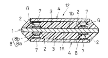
以下、本発明の好ましい実施の形態について図面を参照しながら説明する。図1は本発明の製造方法によって製造できる半導体ベアチップ実装モジュール(半導体装置)12を示す縦断面図であり、同図において、図5と同一若しくは同等のものには同一の符号を付してある。この半導体ベアチップ実装モジュール12では、回路基板1に反り変形が全く生じていなく、それに伴って半導体ベアチップ4のスタッドバンプ8と回路基板1の基板電極2とが位置ずれなく正確な位置決め状態で相互に電気的接続されている。つぎに、このような半導体ベアチップ実装モジュール12を製造することのできる製造方法について説明する。
【0019】
図2(a)〜(g)は本発明の第1の実施の形態に係る半導体装置の製造方法を具現化した製造過程を工程順に示した縦断面図であり、同図において、図1と同一のものには同一の符号を付してある。先ず、同図(a)に示すように、両面の回路上の各所定位置に基板電極2がそれぞれ形成された回路基板1には、これの第1実装面1a上にエポキシからなる熱硬化性接着剤3が塗着される。このとき、熱硬化性接着剤3は第1実装面1aの基板電極2を覆う状態に塗着される。ここで、供給される接着剤3は、導電粒子を含む接着剤または絶縁性の接着剤の何れでもよく、また、形態として、液体もしくはフィルム状の固体の何れであってもよい。
【0020】
一方、同図(b)に示すように、実装すべき半導体ベアチップ4には、その一面に設けられた電極パッド7上に、この電極パッド7に対しこれの素材と融合することにより合金となって強固に固着したバンプ台座部8aと、このバンプ台座部8aの上部に形成されたバンプ頭頂部8bとを有する2段突起形状のスタッドバンプ8が形成されている。この半導体ベアチップ4は、真空吸着ヘッド9に吸着保持されて回路基板1上に搬送されたのち、スタッドバンプ8を基板電極2に位置合わせした状態で熱硬化性接着剤3に軽く押し付けられて、同図(c)に示すように、接着剤3を介し第1実装面1aに仮固定される。
【0021】
上記の半導体ベアチップ4が第1実装面1aに仮固定された回路基板1は、同図(d)に示すように、同じ工程において上下反転されたのち、上面となった第2実装面1b上に熱硬化性接着剤3が塗着される。そののち、同図(e)に示すように、回路基板1の第2実装面1b上には真空吸着ヘッド9に吸着保持された別の半導体ベアチップ4が搬送される。この半導体ベアチップ4は、スタッドバンプ8を基板電極2に対し位置合わせした状態で熱硬化性接着剤3に軽く押し付けられて、接着剤3を介し第2実装面1bに仮固定される。
【0022】
上述のようにして第1および第2実装面1a,1bにそれぞれ半導体ベアチップ4が仮固定された回路基板1は、次工程に搬送されて、同図(f)に示すように、回路基板1の第1および第2実装面1a,1bに仮固定されている2個の半導体ベアチップ4に対し回路基板1の両側から加圧加熱ヘッド10が約30秒間押し付けられながら加熱される。これにより、同図(g)に示すように、回路基板1の両実装面1a,1bに塗着されている熱硬化性接着剤3は同時に熱硬化されて収縮し、この収縮力によって2個の半導体ベアチップ4の全体が回路基板1の対向する実装面1a,1bに引き寄せられて、各スタッドバンプ8のバンプ頭頂部8bは対応する基板電極2にそれぞれ圧着されて電気的に接続される。また、各半導体ベアチップ4は、回路基板1の対向する実装面1a,1bとの隙間全体に充満されて熱硬化した接着剤3によって実装面1a,1bに強固に接着される。これにより、図1に示した半導体ベアチップ実装モジュール12が出来上がる。
【0023】
上記製造方法では、回路基板1の第1および第2実装面1a,1bにそれぞれ半導体ベアチップ4を仮固定している熱硬化性接着剤3を同時に加熱して熱硬化させるので、その熱硬化時における接着剤3中の樹脂の収縮力は、回路基板1の両側実装面1a,1bにおいて均等に、且つ回路基板1に対し互いに反対方向に反りを発生させるよう作用して、互いに打ち消される。その結果、回路基板1には反りの変形が生じない。
【0024】
そのため、第1実装面1aへの実装時だけでなく第2実装面1bへの実装に際しても、回路基板1に反りが存在しない状態で半導体ベアチップ4の仮固定を行えるので、半導体ベアチップ4のスタッドバンプ8と基板電極2とは、第1および第2実装面1a,1bの何れにおいても位置ずれのない正確な位置合わせ状態となって、確実に電気的接続される。さらに、半導体ベアチップ4の圧着工程は、回路基板1に反りの変形が発生するのを防止しながら行えるので、何れの実装面1a,1bにおいてもスタッドバンプ8と基板電極2との接合部に応力が発生せず、接合部の品質低下や接合不良といった不具合が生じることがない。
【0025】
しかも、上記製造方法では、同一工程において回路基板1の第1および第2実装面1a,1bに半導体ベアチップ4を連続的に仮固定するので、従来の製造方法に比較して、半導体ベアチップ4の第1実装面1aに対する加圧加熱による圧着工程から第2実装面1bへ半導体ベアチップ4を仮固定するために再び仮固定工程へ戻すための搬送工程が省略できる。さらに、回路基板1の第1および第2実装面1a,1bへの半導体ベアチップ4の加圧加熱による圧着を同時に行うことから、従来の製造方法に比較して、圧着工程が1回で済む。そのため、上記製造方法は極めて高い生産性で半導体ベアチップ実装モジュール12を製造できる大きな利点もある。
【0026】
図3(a)〜(g)は本発明の第2の実施の形態に係る半導体装置の製造方法を具現化した製造過程を工程順に示した縦断面図であり、同図において、図2と同一のものには同一の符号を付してある。つぎに、この実施の形態の製造工程について、理解を容易にするために、第1の実施の形態と重複する工程の説明をも敢えて含めて説明する。
【0027】
先ず、同図(a)に示すように、回路基板1には、これの第1実装面1a上に熱硬化性接着剤に紫外線硬化性接着剤を混合した混合硬化性接着剤13が塗着される。このとき、混合硬化性接着剤13は第1実装面1aの基板電極2を覆う状態に塗着される。つぎに、同図(b)に示すように、半導体ベアチップ4は、真空吸着ヘッド9に吸着保持されて回路基板1上に搬送されたのち、スタッドバンプ8を基板電極2に位置合わせした状態で混合硬化性接着剤13に軽く押し付けられて、同図(c)に示すように、仮固定される。この仮固定が終了して真空吸着ヘッド9が半導体ベアチップ4から離間したならば、第1実装面1aに半導体ベアチップ4が仮固定された回路基板1は、紫外線照射工程へ向け移載される。その紫外線照射工程では、混合硬化性接着剤13における半導体ベアチップ4よりも外方側に位置する周囲部分に紫外線照射器14から紫外線UVが照射される。これにより、混合硬化性接着剤13の周囲部分には紫外線硬化部13aが形成されて、半導体ベアチップ4と回路基板1との仮固定強度が増強する。
【0028】
上記の半導体ベアチップ4が第1実装面1aに仮固定された回路基板1は、同図(d)に示すように、同じ工程において上下反転される。そののち、同図(e)に示すように、回路基板1の上面となった第2実装面1b上には混合硬化性接着剤13が塗着される。続いて、回路基板1の第2実装面1b上には真空吸着ヘッド9に吸着保持された別の半導体ベアチップ4が搬送されたのち、同図(f)に示すように、スタッドバンプ8を基板電極2に対し位置合わせした状態で混合硬化性接着剤13に軽く押し付けられて仮固定される。なお、第2実装面1bに半導体ベアチップ4を仮固定したのちに、第1実装面1aと同様に、第2実装面1bの混合硬化性接着剤13の周囲に紫外線UVを照射して紫外線硬化部13aを形成するようにしてもよく、紫外線硬化部13aを形成しない場合には、上述の混合硬化性接着剤13に代えて、第2実装面1bに第1の実施の形態で用いた熱硬化性接着剤3を塗着するようにしてもよい。
【0029】
上述のようにして第1および第2実装面1a,1bにそれぞれ半導体ベアチップ4が仮固定された回路基板1は、次工程まで搬送されて、同図(f)に示すように、回路基板1の第1および第2実装面1a,1bに仮固定されている2個の半導体ベアチップ4に対し回路基板1の両側から加圧加熱ヘッド10が約30秒間押し付けられると同時に加熱される。
【0030】
これにより、同図(g)に示すように、回路基板1の両実装面1a,1bに塗着されている混合硬化性接着剤13は同時に熱硬化されて収縮し、この収縮力によって2個の半導体ベアチップ4の全体が回路基板1の対向する実装面1a,1bに引き寄せられて、各スタッドバンプ8のバンプ頭頂部8bは対応する基板電極2にそれぞれ圧着されて電気的に接続される。また、各半導体ベアチップ4は、回路基板1の対向する実装面1a,1bとの隙間全体に充満されて熱硬化した接着剤3によって実装面1a,1bに強固に接着され、これにより、半導体ベアチップ実装モジュール12が出来上がる。
【0031】
上記製造方法においても、第1の実施の形態と同様の効果を得ることができる。すなわち、回路基板1の第1および第2実装面1a,1bにそれぞれ半導体ベアチップ4を仮固定している混合硬化性接着剤13を同時に加熱して熱硬化させるので、その熱硬化時における接着剤13中の樹脂の収縮力は、回路基板1の両側実装面1a,1bにおいて均等に、且つ回路基板1に対し互いに反対方向の反りを発生させるよう作用する結果、互いに打ち消される。したがって、回路基板1には反りの変形が生じない。
【0032】
そのため、第1実装面1aへの実装時だけでなく第2実装面1bへの実装に際しても、回路基板1に反りが存在しない状態で半導体ベアチップ4の仮固定を行えるので、半導体ベアチップ4のスタッドバンプ8と基板電極2とは、第1および第2実装面1a,1bの何れにおいても位置ずれのなく正確な位置合わせ状態となって、確実に電気的接続される。さらに、半導体ベアチップ4の圧着工程は、回路基板1に反りの変形が発生するのを防止しながら行えるので、何れの実装面1a,1bにおいてもスタッドバンプ8と基板電極2との接合部に応力が発生せず、接合部の品質低下や接合不良といった不具合が生じることがない。
【0033】
しかも、上記製造方法では、同一工程において回路基板1の第1および第2実装面1a,1bに半導体ベアチップ4を連続的に仮固定するので、従来の製造方法に比較して、半導体ベアチップ4の第1実装面1aに対する加圧加熱による圧着工程から第2実装面1bへ半導体ベアチップ4を仮固定するために再び仮固定工程へ戻すための搬送工程が省略できる。さらに、回路基板1の第1および第2実装面1a,1bへの半導体ベアチップ4の加圧加熱による圧着を同時に行うことから、従来の製造方法に比較して、圧着工程が1回で済む。そのため、上記製造方法は極めて高い生産性で半導体ベアチップ実装モジュール12を製造できる。
【0034】
この実施の形態では、上記の第1の実施の形態と同様の効果に加えて、回路基板1の第1実装面1aに半導体ベアチップ4を仮固定したのちに、混合硬化性接着剤13の周囲に紫外線UVを照射して紫外線硬化部13aを形成したので、その紫外線硬化部13aによって半導体ベアチップ4と回路基板1との仮固定強度が増強されるから、第1実装面1aへの半導体ベアチップ4の実装が終了した回路基板1を上下反転させる場合および第2実装面1bに半導体ベアチップ4を実装する際の第1実装面1aでの半導体ベアチップ4の回路基板1に対する位置ずれ発生を確実に防止できる利点がある。ここで、回路基板1の両面1a,1bに混合硬化性接着剤13を塗布して、回路基板1の両面1a,1bに紫外線硬化部13aを形成するようにすれば、半導体ベアチップ4の回路基板1に対する位置ずれ発生を一層確実に防止できる。
【0035】
図4(a)〜(g)は本発明の第3の実施の形態に係る半導体装置の製造方法を具現化した製造過程を工程順に示した縦断面図であり、同図において、図3と同一のものには同一の符号を付してある。つぎに、この実施の形態の製造工程について、理解を容易にするために、第2の実施の形態と重複する工程の説明をも敢えて含めて説明する。
【0036】
先ず、同図(a)に示すように、回路基板1には、これの第1実装面1a上に熱硬化性接着剤に紫外線硬化性接着剤を混合した混合硬化性接着剤13が塗着される。このとき、混合硬化性接着剤13は第1実装面1aの基板電極2を覆う状態に塗着される。つぎに、同図(b)に示すように、半導体ベアチップ4は、複合型真空吸着ヘッド17のツール部18に吸着保持されて回路基板1上に搬送されたのち、スタッドバンプ8を基板電極2に位置合わせした状態で混合硬化性接着剤13に軽く押し付けられて、同図(c)に示すように、仮固定される。この仮固定工程と同時に、複合型真空吸着ヘッド17のホルダ部19に取り付けられた紫外線照射器20から混合硬化性接着剤13における半導体ベアチップ4よりも外方側に位置する周囲部分に紫外線UVが照射される。これにより、混合硬化性接着剤13の周囲部分には紫外線硬化部13aが形成されて、半導体ベアチップ4と回路基板1との仮固定強度が増強する。
【0037】
上記の半導体ベアチップ4が第1実装面1aに仮固定された回路基板1は、同図(d)に示すように、同じ工程において上下反転される。そののち、同図(e)に示すように、回路基板1の上面となった第2実装面1b上には混合硬化性接着剤13が塗着される。続いて、回路基板1の第2実装面1b上には複合型真空吸着ヘッド9に吸着保持された別の半導体ベアチップ4が搬送されたのち、同図(c)の図示と同様に、スタッドバンプ8を基板電極2に対し位置合わせした状態で混合硬化性接着剤13に軽く押し付けられて仮固定される。なお、複合型真空吸着ヘッド17で吸着保持している半導体ベアチップ4を第2実装面1bに仮固定するときに、第1実装面1aと同様に、第2実装面1bの混合硬化性接着剤13の周囲に複合型真空吸着ヘッド17の紫外線照射器20から紫外線UVを照射して紫外線硬化部13aを形成するようにしてもよく、この紫外線硬化部13aを形成しない場合には、上述の混合硬化性接着剤13に代えて、第2実装面1bには第1の実施の形態で用いた同様の熱硬化性接着剤3を塗着するようにしてもよい。
【0038】
上述のようにして第1および第2実装面1a,1bにそれぞれ半導体ベアチップ4が仮固定された回路基板1は、次工程まで搬送されて、同図(f)に示すように、回路基板1の第1および第2実装面1a,1bに仮固定されている2個の半導体ベアチップ4に対し回路基板1の両側から加圧加熱ヘッド10が約30秒間押し付けられると同時に加熱される。
【0039】
これにより、同図(g)に示すように、回路基板1の両実装面1a,1bに塗着されている混合硬化性接着剤13は同時に熱硬化されて収縮し、この収縮力によって2個の半導体ベアチップ4の全体が回路基板1の対向する実装面1a,1bに引き寄せられて、各スタッドバンプ8のバンプ頭頂部8bは対応する基板電極2にそれぞれ圧着されて電気的に接続される。また、各半導体ベアチップ4は、回路基板1の対向する実装面1a,1bとの隙間全体に充満されて熱硬化した接着剤13によって実装面1a,1bに強固に接着され、これにより、半導体ベアチップ実装モジュール12が出来上がる。
【0040】
上記製造方法においても、第2の実施の形態と同様の効果を得ることができる。すなわち、回路基板1の第1および第2実装面1a,1bにそれぞれ半導体ベアチップ4を仮固定している混合硬化性接着剤13を同時に加熱して熱硬化させるので、その熱硬化時における接着剤13中の樹脂の収縮力は、回路基板1の両側実装面1a,1bにおいて均等に、且つ回路基板1に対し互いに反対方向の反りを発生させるよう作用する結果、互いに打ち消される。したがって、回路基板1には反りの変形が生じない。
【0041】
そのため、第1実装面1aへの実装時だけでなく第2実装面1bへの実装に際しても、回路基板1に反りが存在しない状態で半導体ベアチップ4の仮固定を行えるので、半導体ベアチップ4のスタッドバンプ8と基板電極2とは、第1および第2実装面1a,1bの何れにおいても位置ずれなく正確な位置合わせ状態となって、確実に電気的接続される。さらに、半導体ベアチップ4の圧着工程は、回路基板1に反りの変形が発生するのを防止しながら行えるので、何れの実装面1a,1bにおいてもスタッドバンプ8と基板電極2との接合部に応力が発生せず、接合部の品質低下や接合不良といった不具合が生じることがない。
【0042】
しかも、上記製造方法では、同一工程において回路基板1の第1および第2実装面1a,1bに半導体ベアチップ4を連続的に仮固定するので、従来の製造方法に比較して、半導体ベアチップ4の第1実装面1aに対する加圧加熱による圧着工程から第2実装面1bへ半導体ベアチップ4を仮固定するために再び仮固定工程へ戻すための搬送工程が省略できる。さらに、回路基板1の第1および第2実装面1a,1bへの半導体ベアチップ4の加圧加熱による圧着を同時に行うことから、従来の製造方法に比較して、圧着工程が1回で済む。そのため、上記製造方法は極めて高い生産性で半導体ベアチップ実装モジュール12を製造できる。
【0043】
また、回路基板1の第1実装面1aに半導体ベアチップ4を仮固定したのちに、混合硬化性接着剤13の周囲に紫外線UVを照射して紫外線硬化部13aを形成したので、その紫外線硬化部13aによって半導体ベアチップ4と回路基板1との仮固定強度が増強されるから、第1実装面1aへの半導体ベアチップ4の実装が終了した回路基板1を上下反転させる場合および第2実装面1bに半導体ベアチップ4を実装する際の第1実装面1aでの半導体ベアチップ4の回路基板1に対する位置ずれ発生を確実に防止できる。
【0044】
この実施の形態では、上記の第2の実施の形態と同様の効果を得られるのに加えて、紫外線照射器20を一体に備えた複合型真空吸着ヘッド17を用いて半導体ベアチップ4を仮固定しながら紫外線UVを同時に照射できるので、第2の実施の形態と比較して、第1実装面1aへの半導体ベアチップ4の仮固定が終了した回路基板1を紫外線照射工程に移載する必要がないので、その分だけ生産性を高めることができるとともに、紫外線照射工程に移載する際の衝撃によって仮固定状態の半導体ベアチップ4の回路基板1に対する位置ずれの発生が生じるおそれがなくなり、接合部の信頼性が一層高まる。複合型真空吸着ヘッド17は紫外線照射器20を一体に備えているから、紫外線照射工程への搬送工程を要することなしに第2実装面1bの混合硬化性接着剤13に紫外線硬化部13aを形成することが可能であり、そのようにした場合には、半導体ベアチップ4の回路基板1に対する位置ずれを一層確実に防止でき、接合部の信頼性がさらに高まる。
【0045】
【発明の効果】
以上のように第1の発明に係る半導体装置の製造方法によれば、回路基板に反りの変形が生じないので、半導体素子に設けた2段突起形状のバンプ、バンプ台座部とバンプ頭頂部からなる2段突起のバンプ、またはバンプ台座部とバンプ頭頂部からなるスタッドバンプと回路基板の基板電極は、回路基板の両面の何れにおいてもバンプ上段が初期高さ未満となる圧着を伴なう位置ずれのない正確な位置合わせ状態での仮固定状態とした上で、バンプ上段が仮固定時の高さ未満となる電気的接続状態への圧着を伴い確実に電気的接続できる。さらに、半導体素子の加熱加圧によるバンプ上段が初期高さ未満となる電気的接続状態への圧着を行う圧着工程は、回路基板に反りの変形が発生するのを防止しながら行えるので、回路基板の両面の何れにおいてもバンプと基板電極との接合部に応力が発生せず、接合部の品質低下や接合不良といった不具合が生じることがない。しかも、同一工程において回路基板の両面に半導体素子を連続的に仮固定できるとともに、回路基板の両面に対し半導体素子の加熱加圧による圧着工程が1回で済むので、極めて高い生産性で半導体装置を製造できる。
【0046】
第2の発明に係る半導体装置の製造方法によれば、第1の発明と同様の効果を得られるのに加えて、半導体素子の回路基板の一面への仮固定時に、接着剤に紫外線硬化部を形成することによって半導体素子と回路基板との仮固定強度が増強されるから、回路基板の一面への半導体素子の実装が終了した回路基板を上下反転させる場合および回路基板の他面に半導体素子を実装する際の一面での半導体素子の回路基板に対する位置ずれ発生を確実に防止できる利点がある。
【図面の簡単な説明】
【図1】本発明の製造方法によって製造できる半導体装置を示す縦断面図。
【図2】(a)〜(g)は本発明の第1の実施の形態に係る半導体装置の製造方法を具現化した製造過程を工程順に示した縦断面図。
【図3】(a)〜(g)は本発明の第2の実施の形態に係る半導体装置の製造方法を具現化した製造過程を工程順に示した縦断面図。
【図4】(a)〜(g)は本発明の第3の実施の形態に係る半導体装置の製造方法を具現化した製造過程を工程順に示した縦断面図。
【図5】(a)〜(g)は、回路基板の両面に半導体ベアチップをフリップチップ方式で実装してなる半導体ベアチップ実装モジュールの従来の製造過程を工程順に示した縦断面図。
【符号の説明】
1 回路基板
1a 第1実装面(一面)
1b 第2実装面(他面)
2 基板電極
3 熱硬化性接着剤
4 半導体ベアチップ(半導体素子)
8 スタッドバンプ(バンプ)
10 加圧加熱ヘッド
12 半導体ベアチップ実装モジュール(半導体装置)
13 混合硬化性接着剤
13a 紫外線硬化部
17 複合型真空吸着ヘッド(吸着ヘッド)
18 ツール部
19 ホルダ部
20 紫外線照射器
UV 紫外線[0001]
The present invention relates to a method of manufacturing a semiconductor device in which a semiconductor bare chip is directly mounted on both sides of a circuit board by a flip chip mounting method. To the law Related to
[0002]
[Prior art]
In recent years, electric devices such as portable information devices are required to be reduced in size and thickness, and accordingly, the mounting density of electronic circuits is required to be increased. As a means for realizing the high density of the electronic circuit, instead of the conventional IC package, the progress of the flip chip type mounting field in which the semiconductor bare chip obtained by dividing the wafer into pieces is turned over and directly mounted on the circuit board is developed. It is remarkable. For example, what is currently produced by the flip chip mounting method is CSP (Chip Size Package) that packages the same size as the semiconductor bare chip and MCM (Multi Chip Module) that mounts multiple semiconductor bare chips on a circuit board. And production by these is increasing. In the SBB (Stud Bump Bondig) method, which is one of the flip chip mounting methods, a bump is formed on the electrode pad of the semiconductor bare chip by applying the wire bonding method, and the height of the bump top of the bump is made uniform. By leveling with this leveling apparatus, a stud bump having a two-step protrusion shape having a bump pedestal portion and a bump top portion is formed.
[0003]
In recent years, development of a technique for mounting a semiconductor bare chip on both sides of a circuit board by a flip chip method has been advanced. FIGS. 5A to 5G are longitudinal sectional views showing a conventional manufacturing process of a semiconductor bare chip mounting module in which semiconductor bare chips are mounted on both surfaces of a circuit board by a flip chip method in the order of steps. First, as shown in FIG. 2A, the
[0004]
On the other hand, as shown in FIG. 2B, the semiconductor
[0005]
The
[0006]
Subsequently, as shown in FIG. 4D, the
[0007]
[Problems to be solved by the invention]
However, in the manufacturing method of the conventional semiconductor bare
[0008]
Therefore, the present invention has been made in view of the above-described conventional problems, and is a semiconductor device capable of mounting semiconductor elements such as semiconductor bare chips on both surfaces of a circuit board with high productivity so as not to cause warping deformation of the circuit board. Manufacturing method The law It is intended to provide.
[0009]
[Means for Solving the Problems]
In order to achieve the above object, a method of manufacturing a semiconductor device according to one aspect of the present invention includes a step of supplying a thermosetting adhesive to one surface of a circuit board, a two-step protrusion-shaped bump provided with a semiconductor element, and a bump A bump with a two-step projection consisting of a pedestal portion and a bump top portion, or a stud bump consisting of a bump pedestal portion and a bump top portion is positioned on the one surface via the adhesive in a positioning state matching the substrate electrode of the circuit board. The upper bump is crimped with deformation that is less than the initial height. A step of temporarily fixing, a step of turning the circuit board on which the semiconductor element is temporarily fixed upside down, a step of supplying a thermosetting adhesive to the other surface of the circuit board, and another semiconductor element are provided. In the positioning state, a bump having a two-step protrusion shape, a bump having a two-step protrusion including a bump pedestal portion and a bump top portion, or a stud bump including a bump pedestal portion and a bump top portion is aligned with the substrate electrode of the circuit board. On the other side through the agent The upper bump is crimped with deformation that is less than the initial height. Temporarily fixing the adhesive on both sides of the circuit board simultaneously by heating while pressing each semiconductor element temporarily fixed on both sides of the circuit board in a direction to press the circuit board against the circuit board. And the bumps of the respective semiconductor elements are arranged on the substrate electrodes facing the circuit board. Temporarily fixed And a step of crimping to an electrical connection state that is less than the height.
[0010]
In this method of manufacturing a semiconductor device, since the thermosetting adhesive temporarily fixing the semiconductor elements on both sides of the circuit board is simultaneously heated and thermally cured, the shrinkage force of the resin in the adhesive during the thermosetting Are counteracted by acting on both sides of the circuit board evenly and in a direction opposite to each other to generate warpage. As a result, warping deformation does not occur in the circuit board, so that a bump with a two-step protrusion provided on the semiconductor element, a bump with a two-step protrusion comprising a bump pedestal portion and a bump top portion, or a bump pedestal portion and a bump top portion The stud bump made of and the substrate electrode of the circuit board are both on both sides of the circuit board. Accompanied by crimping where the upper bump is below the initial height Accurate alignment without misalignment Temporary fixing And the upper bump is Furthermore, at the time of temporary fixing Electrical connection can be ensured with crimping to an electrical connection state of less than the height. Further, the crimping step of crimping the bump upper stage by heating and pressurizing the semiconductor element to an electrical connection state where the initial height is less than the initial height can be performed while preventing the warp deformation of the circuit board. No stress is generated at the joint between the bump and the substrate electrode on both surfaces, and there is no problem such as deterioration in the quality of the joint or poor bonding. In addition, the semiconductor elements can be temporarily fixed on both sides of the circuit board in the same process, and the crimping process by heating and pressurizing the semiconductor elements on both sides of the circuit board can be performed only once, so that the semiconductor device can be manufactured with extremely high productivity. Can be manufactured.
[0011]
According to other inventions The manufacturing method of the semiconductor device is as follows: Supplying a mixed curable adhesive, which is a mixture of thermosetting and ultraviolet curable adhesives, to one surface of the circuit board; a bump having a two-stage protrusion having a semiconductor element provided thereon; a bump pedestal and a bump head The bumps of the two-step projections formed from the top, or the stud bumps formed from the bump pedestal and the bump top are positioned on the one surface through the adhesive in a positioning state matching the substrate electrode of the circuit board. The upper bump is crimped with deformation that is less than the initial height. A step of temporarily fixing, a step of irradiating ultraviolet rays around the adhesive to form an ultraviolet curing portion only around the adhesive, and an inversion of the circuit board on which the semiconductor element is temporarily fixed A step of supplying a thermosetting adhesive to the other surface of the circuit board, a bump having a two-step projection provided with another semiconductor element, and a two-step projection comprising a bump pedestal portion and a bump top portion. A bump, or a stud bump consisting of a bump pedestal and a bump top, is positioned on the other surface through the thermosetting adhesive in a positioning state that matches the substrate electrode of the circuit board. The upper bump is crimped with deformation that is less than the initial height. Temporarily fixing the adhesive on both sides of the circuit board simultaneously by heating while pressing each semiconductor element temporarily fixed on both sides of the circuit board in a direction to press the circuit board against the circuit board. And the bumps of the respective semiconductor elements are bumped on the substrate electrodes facing the circuit board. Temporarily fixed And a step of crimping to an electrical connection state that is less than the height.
[0012]
In this method of manufacturing a semiconductor device, in addition to obtaining the same effect as the first invention, the temporary fixing strength between the semiconductor element and the circuit board is enhanced by the ultraviolet curing part. There is an advantage that it is possible to reliably prevent the occurrence of displacement of the semiconductor element with respect to the circuit board on one side when the circuit board on which the semiconductor element has been mounted is turned upside down and when the semiconductor element is mounted on the other side of the circuit board.
[0015]
The semiconductor device of the present invention is formed by mounting semiconductor elements on both sides of a circuit board by the manufacturing method according to the above-described invention or another invention. In this semiconductor device, the circuit board is not warped and deformed, and accordingly, the bumps of the semiconductor element and the substrate electrodes of the circuit board are electrically connected to each other in an accurate positioning state without displacement.
[0018]
DETAILED DESCRIPTION OF THE INVENTION
Hereinafter, preferred embodiments of the present invention will be described with reference to the drawings. FIG. 1 is a longitudinal sectional view showing a semiconductor bare chip mounting module (semiconductor device) 12 that can be manufactured by the manufacturing method of the present invention. In FIG. 1, the same or equivalent parts as those in FIG. . In this semiconductor bare
[0019]
2 (a) to 2 (g) are longitudinal sectional views showing a manufacturing process embodying the manufacturing method of the semiconductor device according to the first embodiment of the present invention in the order of steps, in which FIG. The same code | symbol is attached | subjected to the same thing. First, as shown in FIG. 2A, the
[0020]
On the other hand, as shown in FIG. 2B, the semiconductor
[0021]
The
[0022]
The
[0023]
In the above manufacturing method, the
[0024]
Therefore, the semiconductor
[0025]
In addition, in the above manufacturing method, the semiconductor
[0026]
3 (a) to 3 (g) are longitudinal sectional views showing a manufacturing process embodying a manufacturing method of a semiconductor device according to the second embodiment of the present invention in the order of steps, in which FIG. The same code | symbol is attached | subjected to the same thing. Next, in order to facilitate understanding of the manufacturing process of this embodiment, a description of the same process as that of the first embodiment will be given.
[0027]
First, as shown in FIG. 2A, a mixed curable adhesive 13 in which an ultraviolet curable adhesive is mixed with a thermosetting adhesive is applied to the
[0028]
The
[0029]
The
[0030]
As a result, as shown in FIG. 5G, the mixed
[0031]
Also in the manufacturing method, the same effect as that of the first embodiment can be obtained. That is, since the mixed
[0032]
Therefore, the semiconductor
[0033]
In addition, in the above manufacturing method, the semiconductor
[0034]
In this embodiment, in addition to the same effects as those of the first embodiment, the semiconductor
[0035]
4 (a) to 4 (g) are longitudinal sectional views showing a manufacturing process embodying a manufacturing method of a semiconductor device according to the third embodiment of the present invention in the order of steps, in which FIG. The same code | symbol is attached | subjected to the same thing. Next, in order to facilitate understanding of the manufacturing process of this embodiment, a description of the same process as that of the second embodiment is also included.
[0036]
First, as shown in FIG. 2A, a mixed curable adhesive 13 in which an ultraviolet curable adhesive is mixed with a thermosetting adhesive is applied to the
[0037]
The
[0038]
The
[0039]
As a result, as shown in FIG. 5G, the mixed
[0040]
Also in the manufacturing method, the same effect as in the second embodiment can be obtained. That is, since the mixed
[0041]
Therefore, the semiconductor
[0042]
Moreover, in the above manufacturing method, the semiconductor
[0043]
In addition, after the semiconductor
[0044]
In this embodiment, in addition to obtaining the same effect as in the second embodiment, the semiconductor
[0045]
【The invention's effect】
As described above, according to the method for manufacturing a semiconductor device according to the first aspect of the present invention, warping deformation does not occur in the circuit board. The bumps of the two-step projections, or the stud bumps consisting of the bump pedestal portion and the bump top portion, and the substrate electrodes of the circuit board, both on both sides of the circuit board Accompanied by crimping where the upper bump is below the initial height Accurate alignment without misalignment In the temporarily fixed state in , The upper bump is Temporarily fixed Electrical connection can be ensured with crimping to an electrical connection state of less than the height. Furthermore, the crimping process for crimping the bumps to the electrical connection state where the bump upper stage by heating and pressing of the semiconductor element is less than the initial height can be performed while preventing the warp deformation from occurring in the circuit board. No stress is generated at the joint between the bump and the substrate electrode on any of the two surfaces, and there is no problem such as deterioration in the quality of the joint or poor bonding. In addition, the semiconductor elements can be temporarily fixed on both sides of the circuit board in the same process, and the crimping process by heating and pressurizing the semiconductor elements on both sides of the circuit board can be performed only once, so that the semiconductor device can be manufactured with extremely high productivity. Can be manufactured.
[0046]
According to the method for manufacturing a semiconductor device according to the second invention, in addition to obtaining the same effect as in the first invention, the ultraviolet curing portion is attached to the adhesive when temporarily fixing the semiconductor element to one surface of the circuit board. Since the temporary fixing strength between the semiconductor element and the circuit board is enhanced by forming the circuit board, when the circuit board after mounting the semiconductor element on one surface of the circuit board is turned upside down, and the semiconductor element on the other surface of the circuit board There is an advantage that it is possible to reliably prevent the occurrence of displacement of the semiconductor element with respect to the circuit board on one surface when mounting.
[Brief description of the drawings]
FIG. 1 is a longitudinal sectional view showing a semiconductor device that can be manufactured by a manufacturing method of the present invention.
FIGS. 2A to 2G are longitudinal sectional views showing a manufacturing process embodying a manufacturing method of a semiconductor device according to a first embodiment of the present invention in order of steps;
FIGS. 3A to 3G are longitudinal sectional views showing a manufacturing process embodying a semiconductor device manufacturing method according to a second embodiment of the present invention in the order of steps;
FIGS. 4A to 4G are longitudinal sectional views showing a manufacturing process embodying a manufacturing method of a semiconductor device according to a third embodiment of the present invention in the order of steps;
FIGS. 5A to 5G are longitudinal sectional views showing a conventional manufacturing process of a semiconductor bare chip mounting module in which a semiconductor bare chip is mounted on both sides of a circuit board by a flip chip method in order of steps;
[Explanation of symbols]
1 Circuit board
1a First mounting surface (one surface)
1b Second mounting surface (other surface)
2 Substrate electrode
3 Thermosetting adhesive
4 Semiconductor bare chip (semiconductor element)
8 Stud bump (bump)
10 Pressure heating head
12 Semiconductor bare chip mounting module (semiconductor device)
13 Mixed curable adhesive
13a UV curing part
17 Combined vacuum suction head (Suction head)
18 Tool part
19 Holder part
20 UV irradiator
UV UV
Claims (2)
半導体素子をこれに設けた2段突起形状のバンプ、バンプ台座部とバンプ頭頂部からなる2段突起のバンプ、またはバンプ台座部とバンプ頭頂部からなるスタッドバンプが前記回路基板の基板電極に合致する位置決め状態で前記接着剤を介し前記一面にバンプ上段が初期高さ未満となる変形を伴い圧着し仮固定する工程と、
前記半導体素子が仮固定された前記回路基板を上下反転させる工程と、
前記回路基板の他面に熱硬化性接着剤を供給する工程と、
別の半導体素子をこれに設けた2段突起形状のバンプ、バンプ台座部とバンプ頭頂部からなる2段突起のバンプ、またはバンプ台座部とバンプ頭頂部からなるスタッドバンプが前記回路基板の基板電極に合致する位置決め状態で前記接着剤を介し前記他面にバンプ上段が初期高さ未満となる変形を伴い圧着し仮固定する工程と、
前記回路基板の両面に仮固定された前記各半導体素子をそれぞれ前記回路基板に押し付ける方向に加圧しながら加熱することにより前記回路基板の両面側の前記接着剤を同時に熱硬化させて、前記各半導体素子の各々の前記バンプを前記回路基板の対向する前記基板電極にバンプ上段が仮固定時の高さ未満となる電気的接続状態に圧着する工程とを備えていることを特徴とする半導体装置の製造方法。Supplying a thermosetting adhesive to one surface of the circuit board;
A bump with a two-step projection provided with a semiconductor element, a bump with a two-step projection consisting of a bump pedestal and a bump top, or a stud bump consisting of a bump pedestal and a bump top matches the substrate electrode of the circuit board. A step of crimping and temporarily fixing the upper surface of the bump with a deformation that is less than the initial height via the adhesive in the positioning state to be performed ;
Reversing the circuit board on which the semiconductor element is temporarily fixed;
Supplying a thermosetting adhesive to the other surface of the circuit board;
A bump of a two-step projection provided with another semiconductor element, a bump of a two-step projection consisting of a bump pedestal portion and a bump top portion, or a stud bump consisting of a bump pedestal portion and a bump top portion is a substrate electrode of the circuit board. A step of crimping and temporarily fixing the bump upper stage to the other surface with a deformation that is less than the initial height through the adhesive in a positioning state that conforms to:
The respective semiconductor elements temporarily fixed on both sides of the circuit board are heated while being pressed in a direction in which the semiconductor elements are pressed against the circuit board, thereby simultaneously thermosetting the adhesive on both sides of the circuit board, and thereby each of the semiconductors. A step of crimping each bump of each element to the substrate electrode facing the circuit board in an electrical connection state in which an upper stage of the bump is less than a height when temporarily fixed . Production method.
半導体素子をこれに設けた2段突起形状のバンプ、バンプ台座部とバンプ頭頂部からなる2段突起のバンプ、またはバンプ台座部とバンプ頭頂部からなるスタッドバンプが前記回路基板の基板電極に合致する位置決め状態で前記接着剤を介し前記一面にバンプ上段が初期高さ未満となる変形を伴い圧着し仮固定する工程と、
前記接着剤の周囲に紫外線を照射して前記接着剤のうちの周囲にのみ紫外線硬化部を形成する工程と、
前記半導体素子が仮固定された前記回路基板を上下反転させる工程と、
前記回路基板の他面に熱硬化性接着剤を供給する工程と、
別の半導体素子をこれに設けた2段突起形状のバンプ、バンプ台座部とバンプ頭頂部からなる2段突起のバンプ、またはバンプ台座部とバンプ頭頂部からなるスタッドバンプが前記回路基板の基板電極に合致する位置決め状態で前記熱硬化性接着剤を介し前記他面にバンプ上段が初期高さ未満となる変形を伴い圧着し仮固定する工程と、
前記回路基板の両面に仮固定された前記各半導体素子をそれぞれ前記回路基板に押し付ける方向に加圧しながら加熱することにより前記回路基板の両面側の前記接着剤を同時に熱硬化させて、前記各半導体素子の各々のバンプを前記回路基板の対向する前記基板電極にバンプ上段が仮固定時の高さ未満となる電気的接続状態に圧着する工程とを備えていることを特徴とする半導体装置の製造方法。Supplying a mixed curable adhesive, which is a mixture of thermosetting and ultraviolet curable adhesives, to one surface of the circuit board;
A bump with a two-step projection provided with a semiconductor element, a bump with a two-step projection consisting of a bump pedestal and a bump top, or a stud bump consisting of a bump pedestal and a bump top matches the substrate electrode of the circuit board. A step of crimping and temporarily fixing the upper surface of the bump with a deformation that is less than the initial height via the adhesive in the positioning state to be performed ;
Irradiating ultraviolet rays around the adhesive to form an ultraviolet curing part only around the adhesive; and
Reversing the circuit board on which the semiconductor element is temporarily fixed;
Supplying a thermosetting adhesive to the other surface of the circuit board;
A bump of a two-step projection provided with another semiconductor element, a bump of a two-step projection consisting of a bump pedestal portion and a bump top portion, or a stud bump consisting of a bump pedestal portion and a bump top portion is a substrate electrode of the circuit board. A step of crimping and temporarily fixing the upper surface of the bump with deformation that is less than the initial height via the thermosetting adhesive in a positioning state that matches
The respective semiconductor elements temporarily fixed on both sides of the circuit board are heated while being pressed in a direction in which the semiconductor elements are pressed against the circuit board, thereby simultaneously thermosetting the adhesive on both sides of the circuit board, and thereby each of the semiconductors. And a step of crimping each bump of the element to the substrate electrode facing the circuit board in an electrically connected state in which the upper stage of the bump is less than the height when temporarily fixed. Method.
Priority Applications (2)
| Application Number | Priority Date | Filing Date | Title |
|---|---|---|---|
| JP2001392970A JP3914431B2 (en) | 2001-12-26 | 2001-12-26 | Manufacturing method of semiconductor device |
| US10/328,189 US6966964B2 (en) | 2001-12-26 | 2002-12-26 | Method and apparatus for manufacturing semiconductor device |
Applications Claiming Priority (1)
| Application Number | Priority Date | Filing Date | Title |
|---|---|---|---|
| JP2001392970A JP3914431B2 (en) | 2001-12-26 | 2001-12-26 | Manufacturing method of semiconductor device |
Publications (3)
| Publication Number | Publication Date |
|---|---|
| JP2003197853A JP2003197853A (en) | 2003-07-11 |
| JP2003197853A5 JP2003197853A5 (en) | 2005-07-28 |
| JP3914431B2 true JP3914431B2 (en) | 2007-05-16 |
Family
ID=19188732
Family Applications (1)
| Application Number | Title | Priority Date | Filing Date |
|---|---|---|---|
| JP2001392970A Expired - Fee Related JP3914431B2 (en) | 2001-12-26 | 2001-12-26 | Manufacturing method of semiconductor device |
Country Status (2)
| Country | Link |
|---|---|
| US (1) | US6966964B2 (en) |
| JP (1) | JP3914431B2 (en) |
Families Citing this family (14)
| Publication number | Priority date | Publication date | Assignee | Title |
|---|---|---|---|---|
| JP2006154655A (en) * | 2004-12-01 | 2006-06-15 | Bridgestone Corp | Method for manufacturing information display panel, and information display apparatus |
| KR100598459B1 (en) | 2004-12-10 | 2006-07-11 | 주식회사 쎄크 | Chip bonding apparatus |
| WO2006070863A1 (en) * | 2004-12-28 | 2006-07-06 | Matsushita Electric Industrial Co., Ltd. | Semiconductor chip mounting structure and method for manufacturing same |
| JP2006210566A (en) * | 2005-01-27 | 2006-08-10 | Akita Denshi Systems:Kk | Semiconductor device |
| US7170183B1 (en) * | 2005-05-13 | 2007-01-30 | Amkor Technology, Inc. | Wafer level stacked package |
| DE102007010731A1 (en) * | 2007-02-26 | 2008-08-28 | Würth Elektronik GmbH & Co. KG | Method for arranging electronic chip in circuit board, involves forming of cavity in circuit board and base of cavity is structured for forming connection point |
| JP4952353B2 (en) * | 2007-04-18 | 2012-06-13 | パナソニック株式会社 | Chip module and memory card |
| JP5179787B2 (en) * | 2007-06-22 | 2013-04-10 | ラピスセミコンダクタ株式会社 | Semiconductor device and manufacturing method thereof |
| JP2009049051A (en) * | 2007-08-14 | 2009-03-05 | Elpida Memory Inc | Bonding method of semiconductor substrate and laminate manufactured thereby |
| JP2010062365A (en) * | 2008-09-04 | 2010-03-18 | Hitachi Ltd | Semiconductor device and method of manufacturing the same |
| US8710654B2 (en) | 2011-05-26 | 2014-04-29 | Kabushiki Kaisha Toshiba | Semiconductor device and manufacturing method thereof |
| US9252130B2 (en) * | 2013-03-29 | 2016-02-02 | Stats Chippac, Ltd. | Methods of manufacturing flip chip semiconductor packages using double-sided thermal compression bonding |
| FR3011679B1 (en) * | 2013-10-03 | 2017-01-27 | Commissariat Energie Atomique | IMPROVED METHOD FOR DIRECT COLLAR ASSEMBLY BETWEEN TWO ELEMENTS, EACH ELEMENT COMPRISING METAL PORTIONS AND DIELECTRIC MATERIALS |
| JP6189181B2 (en) | 2013-11-06 | 2017-08-30 | 東芝メモリ株式会社 | Manufacturing method of semiconductor device |
Family Cites Families (4)
| Publication number | Priority date | Publication date | Assignee | Title |
|---|---|---|---|---|
| US5366933A (en) * | 1993-10-13 | 1994-11-22 | Intel Corporation | Method for constructing a dual sided, wire bonded integrated circuit chip package |
| JP3266815B2 (en) * | 1996-11-26 | 2002-03-18 | シャープ株式会社 | Method for manufacturing semiconductor integrated circuit device |
| US6071371A (en) * | 1998-02-02 | 2000-06-06 | Delco Electronics Corporation | Method of simultaneously attaching surface-mount and chip-on-board dies to a circuit board |
| JP2002198395A (en) * | 2000-12-26 | 2002-07-12 | Seiko Epson Corp | Semiconductor device, its manufacturing method, circuit board, and electronic appliance |
-
2001
- 2001-12-26 JP JP2001392970A patent/JP3914431B2/en not_active Expired - Fee Related
-
2002
- 2002-12-26 US US10/328,189 patent/US6966964B2/en not_active Expired - Fee Related
Also Published As
| Publication number | Publication date |
|---|---|
| US6966964B2 (en) | 2005-11-22 |
| US20030138993A1 (en) | 2003-07-24 |
| JP2003197853A (en) | 2003-07-11 |
Similar Documents
| Publication | Publication Date | Title |
|---|---|---|
| EP1445995B1 (en) | Method of mounting an electronic component on a circuit board and system for carrying out the method | |
| JP2833326B2 (en) | Electronic component mounted connector and method of manufacturing the same | |
| US6724080B1 (en) | Heat sink with elevated heat spreader lid | |
| JP3914431B2 (en) | Manufacturing method of semiconductor device | |
| JP4663184B2 (en) | Manufacturing method of semiconductor device | |
| US8138018B2 (en) | Manufacturing method of semiconductor device having underfill resin formed without void between semiconductor chip and wiring board | |
| JP3326382B2 (en) | Method for manufacturing semiconductor device | |
| JP2004356529A (en) | Semiconductor device and method for manufacturing the semiconductor device | |
| US6773958B1 (en) | Integrated assembly-underfill flip chip process | |
| WO2004064142A1 (en) | Semiconductor device and process for producing the same | |
| JP3552422B2 (en) | Ball grid array semiconductor device and its mounting method | |
| JP2002359323A (en) | Semiconductor device and its manufacturing method | |
| JP2001257239A (en) | Manufacturing method of semiconductor device | |
| JP2000286302A (en) | Method and device for assembling semiconductor chip | |
| JP2002184936A (en) | Semiconductor device and its manufacturing method | |
| JPH10154726A (en) | Semiconductor device and its manufacture | |
| JP2002026071A (en) | Semiconductor device and its manufacturing method, circuit board, and electronic equipment | |
| JP3539528B2 (en) | Semiconductor device and manufacturing method thereof | |
| JP2002299809A (en) | Electronic component mounting method and equipment | |
| JP3947502B2 (en) | Manufacturing method of sealing member made of anisotropic conductive film | |
| JP2002026250A (en) | Manufacturing method of laminated circuit module | |
| JPH11274227A (en) | Method and device for mounting semiconductor chip | |
| JP4628234B2 (en) | Crimping apparatus and crimping method | |
| JP3419398B2 (en) | Method for manufacturing semiconductor device | |
| JP2002016104A (en) | Mounting method of semiconductor device and manufacturing method of semiconductor device mounted assembly |
Legal Events
| Date | Code | Title | Description |
|---|---|---|---|
| A521 | Written amendment |
Free format text: JAPANESE INTERMEDIATE CODE: A523 Effective date: 20041210 |
|
| A621 | Written request for application examination |
Free format text: JAPANESE INTERMEDIATE CODE: A621 Effective date: 20041210 |
|
| A977 | Report on retrieval |
Free format text: JAPANESE INTERMEDIATE CODE: A971007 Effective date: 20060522 |
|
| A131 | Notification of reasons for refusal |
Free format text: JAPANESE INTERMEDIATE CODE: A131 Effective date: 20060530 |
|
| A521 | Written amendment |
Free format text: JAPANESE INTERMEDIATE CODE: A523 Effective date: 20060727 |
|
| A02 | Decision of refusal |
Free format text: JAPANESE INTERMEDIATE CODE: A02 Effective date: 20060822 |
|
| A521 | Written amendment |
Free format text: JAPANESE INTERMEDIATE CODE: A523 Effective date: 20061010 |
|
| A911 | Transfer to examiner for re-examination before appeal (zenchi) |
Free format text: JAPANESE INTERMEDIATE CODE: A911 Effective date: 20061116 |
|
| TRDD | Decision of grant or rejection written | ||
| A01 | Written decision to grant a patent or to grant a registration (utility model) |
Free format text: JAPANESE INTERMEDIATE CODE: A01 Effective date: 20070116 |
|
| A61 | First payment of annual fees (during grant procedure) |
Free format text: JAPANESE INTERMEDIATE CODE: A61 Effective date: 20070202 |
|
| R150 | Certificate of patent or registration of utility model |
Free format text: JAPANESE INTERMEDIATE CODE: R150 |
|
| FPAY | Renewal fee payment (event date is renewal date of database) |
Free format text: PAYMENT UNTIL: 20100209 Year of fee payment: 3 |
|
| FPAY | Renewal fee payment (event date is renewal date of database) |
Free format text: PAYMENT UNTIL: 20110209 Year of fee payment: 4 |
|
| FPAY | Renewal fee payment (event date is renewal date of database) |
Free format text: PAYMENT UNTIL: 20120209 Year of fee payment: 5 |
|
| FPAY | Renewal fee payment (event date is renewal date of database) |
Free format text: PAYMENT UNTIL: 20130209 Year of fee payment: 6 |
|
| LAPS | Cancellation because of no payment of annual fees |