CN1058809C - 制造cmos晶体管的方法 - Google Patents
制造cmos晶体管的方法 Download PDFInfo
- Publication number
- CN1058809C CN1058809C CN96113302A CN96113302A CN1058809C CN 1058809 C CN1058809 C CN 1058809C CN 96113302 A CN96113302 A CN 96113302A CN 96113302 A CN96113302 A CN 96113302A CN 1058809 C CN1058809 C CN 1058809C
- Authority
- CN
- China
- Prior art keywords
- coupling part
- gate electrode
- trap
- transistor
- common gate
- Prior art date
- Legal status (The legal status is an assumption and is not a legal conclusion. Google has not performed a legal analysis and makes no representation as to the accuracy of the status listed.)
- Expired - Fee Related
Links
- 238000004519 manufacturing process Methods 0.000 title abstract 2
- 239000002184 metal Substances 0.000 claims abstract description 16
- 238000000034 method Methods 0.000 claims abstract description 14
- 229910021420 polycrystalline silicon Inorganic materials 0.000 claims abstract description 10
- 229920005591 polysilicon Polymers 0.000 claims abstract description 9
- 230000015572 biosynthetic process Effects 0.000 claims abstract description 8
- 230000008878 coupling Effects 0.000 claims description 28
- 238000010168 coupling process Methods 0.000 claims description 28
- 238000005859 coupling reaction Methods 0.000 claims description 28
- 238000005516 engineering process Methods 0.000 claims description 21
- 239000000758 substrate Substances 0.000 claims description 8
- 239000011229 interlayer Substances 0.000 claims description 4
- 230000003647 oxidation Effects 0.000 claims description 4
- 238000007254 oxidation reaction Methods 0.000 claims description 4
- 238000002955 isolation Methods 0.000 claims 4
- 230000003071 parasitic effect Effects 0.000 abstract description 6
- 238000002347 injection Methods 0.000 description 5
- 239000007924 injection Substances 0.000 description 5
- 238000000926 separation method Methods 0.000 description 3
- 230000004888 barrier function Effects 0.000 description 2
- 239000000203 mixture Substances 0.000 description 2
- 238000012797 qualification Methods 0.000 description 2
- 241000282376 Panthera tigris Species 0.000 description 1
- 230000000295 complement effect Effects 0.000 description 1
- 238000005137 deposition process Methods 0.000 description 1
- 239000012535 impurity Substances 0.000 description 1
- 229910044991 metal oxide Inorganic materials 0.000 description 1
- 150000004706 metal oxides Chemical class 0.000 description 1
- 239000004065 semiconductor Substances 0.000 description 1
Images

Classifications
-
- H—ELECTRICITY
- H01—ELECTRIC ELEMENTS
- H01L—SEMICONDUCTOR DEVICES NOT COVERED BY CLASS H10
- H01L29/00—Semiconductor devices specially adapted for rectifying, amplifying, oscillating or switching and having potential barriers; Capacitors or resistors having potential barriers, e.g. a PN-junction depletion layer or carrier concentration layer; Details of semiconductor bodies or of electrodes thereof ; Multistep manufacturing processes therefor
- H01L29/66—Types of semiconductor device ; Multistep manufacturing processes therefor
- H01L29/68—Types of semiconductor device ; Multistep manufacturing processes therefor controllable by only the electric current supplied, or only the electric potential applied, to an electrode which does not carry the current to be rectified, amplified or switched
- H01L29/70—Bipolar devices
- H01L29/72—Transistor-type devices, i.e. able to continuously respond to applied control signals
- H01L29/739—Transistor-type devices, i.e. able to continuously respond to applied control signals controlled by field-effect, e.g. bipolar static induction transistors [BSIT]
-
- H—ELECTRICITY
- H01—ELECTRIC ELEMENTS
- H01L—SEMICONDUCTOR DEVICES NOT COVERED BY CLASS H10
- H01L21/00—Processes or apparatus adapted for the manufacture or treatment of semiconductor or solid state devices or of parts thereof
- H01L21/70—Manufacture or treatment of devices consisting of a plurality of solid state components formed in or on a common substrate or of parts thereof; Manufacture of integrated circuit devices or of parts thereof
- H01L21/77—Manufacture or treatment of devices consisting of a plurality of solid state components or integrated circuits formed in, or on, a common substrate
- H01L21/78—Manufacture or treatment of devices consisting of a plurality of solid state components or integrated circuits formed in, or on, a common substrate with subsequent division of the substrate into plural individual devices
- H01L21/82—Manufacture or treatment of devices consisting of a plurality of solid state components or integrated circuits formed in, or on, a common substrate with subsequent division of the substrate into plural individual devices to produce devices, e.g. integrated circuits, each consisting of a plurality of components
- H01L21/822—Manufacture or treatment of devices consisting of a plurality of solid state components or integrated circuits formed in, or on, a common substrate with subsequent division of the substrate into plural individual devices to produce devices, e.g. integrated circuits, each consisting of a plurality of components the substrate being a semiconductor, using silicon technology
- H01L21/8232—Field-effect technology
- H01L21/8234—MIS technology, i.e. integration processes of field effect transistors of the conductor-insulator-semiconductor type
- H01L21/8238—Complementary field-effect transistors, e.g. CMOS
- H01L21/823871—Complementary field-effect transistors, e.g. CMOS interconnection or wiring or contact manufacturing related aspects
-
- H—ELECTRICITY
- H01—ELECTRIC ELEMENTS
- H01L—SEMICONDUCTOR DEVICES NOT COVERED BY CLASS H10
- H01L27/00—Devices consisting of a plurality of semiconductor or other solid-state components formed in or on a common substrate
- H01L27/02—Devices consisting of a plurality of semiconductor or other solid-state components formed in or on a common substrate including semiconductor components specially adapted for rectifying, oscillating, amplifying or switching and having potential barriers; including integrated passive circuit elements having potential barriers
- H01L27/04—Devices consisting of a plurality of semiconductor or other solid-state components formed in or on a common substrate including semiconductor components specially adapted for rectifying, oscillating, amplifying or switching and having potential barriers; including integrated passive circuit elements having potential barriers the substrate being a semiconductor body
- H01L27/08—Devices consisting of a plurality of semiconductor or other solid-state components formed in or on a common substrate including semiconductor components specially adapted for rectifying, oscillating, amplifying or switching and having potential barriers; including integrated passive circuit elements having potential barriers the substrate being a semiconductor body including only semiconductor components of a single kind
- H01L27/085—Devices consisting of a plurality of semiconductor or other solid-state components formed in or on a common substrate including semiconductor components specially adapted for rectifying, oscillating, amplifying or switching and having potential barriers; including integrated passive circuit elements having potential barriers the substrate being a semiconductor body including only semiconductor components of a single kind including field-effect components only
- H01L27/088—Devices consisting of a plurality of semiconductor or other solid-state components formed in or on a common substrate including semiconductor components specially adapted for rectifying, oscillating, amplifying or switching and having potential barriers; including integrated passive circuit elements having potential barriers the substrate being a semiconductor body including only semiconductor components of a single kind including field-effect components only the components being field-effect transistors with insulated gate
- H01L27/092—Devices consisting of a plurality of semiconductor or other solid-state components formed in or on a common substrate including semiconductor components specially adapted for rectifying, oscillating, amplifying or switching and having potential barriers; including integrated passive circuit elements having potential barriers the substrate being a semiconductor body including only semiconductor components of a single kind including field-effect components only the components being field-effect transistors with insulated gate complementary MIS field-effect transistors
- H01L27/0921—Means for preventing a bipolar, e.g. thyristor, action between the different transistor regions, e.g. Latchup prevention
Landscapes
- Engineering & Computer Science (AREA)
- Power Engineering (AREA)
- Microelectronics & Electronic Packaging (AREA)
- Physics & Mathematics (AREA)
- Condensed Matter Physics & Semiconductors (AREA)
- General Physics & Mathematics (AREA)
- Computer Hardware Design (AREA)
- Manufacturing & Machinery (AREA)
- Ceramic Engineering (AREA)
- Metal-Oxide And Bipolar Metal-Oxide Semiconductor Integrated Circuits (AREA)
Abstract
本发明涉及一种制造CMOS晶体管的方法,能进一步减少芯片的尺寸,因为PMOS晶体管的栅电极和NMOS晶体管的栅电极,在形成栅电极工艺的期间,直接由多晶硅相互连接,不需要考虑金属接触工艺的袼度,该方法还能利用在多晶硅布线下面的有源区形成单元间隔区,防止寄生晶体管的形成。
Description
本发明涉及制造互补金属氧化物(CMOS)的方法,特别是涉及制造CMOS晶体管的方法,它能防止在PMOS晶体管和NMOS晶体管之间形成寄生晶体管,并且减小芯片的尺寸。
通常,按下述方法制造CMOS晶体管,即在P衬底的部分形成N-阱、在N-阱中形成PMOS晶体管,在P-衬底中形成NMOS晶体管。然后互连PMOS晶体管的栅极和NMOS晶体管的栅极。通常,用多晶硅形成栅电极。在CMOS晶体管运作过程中,由于发生闭锁现象,降低晶体管的可靠性。为了防止闭锁现象发生,在隔离元件以便限定场区和有源区的工艺中,通过制作包括在有源区中的N-阱边缘部分和把N+杂质注入到N-阱边缘部分的有源区,形成收集区(Pick-up)区。如上所述,在沿N-阱边缘形成收集区的情况,互连PMOS晶体管栅极和NMOS晶体管栅极的布线越过收集区在布线和收集区之间形绝缘层。在由形成栅电极的多晶硅形成布线的情况,存在下述缺点,在其间有绝缘层的多晶硅布线和收集区作为寄生晶体管,因此,它降低了CMOS晶体管的性能。下面参照图1、图2A和图2B叙述克服上述缺点的方法。
图1是现有技术CMOS晶体管的布图,图2A是沿图1的X-X′线剖开的剖视图。图2B是沿图1中Y-Y′线剖开的剖视图。
参看图1,图2A和图2B。在部分P-衬底1中形成N-阱11。通过元件隔离工艺限定场区和有源区以后,利用氧化工艺在场区形成场氧化膜2。在N-阱中形成PMOS晶体管10,在P-衬底1中形成NMOS晶体管20。PMOS晶体管10包括第1栅电极12,源和漏的第1和第2连接部分13A和13B。NMOS晶体管20包括第2栅电极22和源及漏的第3与第4连接部分23A和23B。分别通过多晶硅淀积工艺和构图工艺形成第1和第2栅电极12与22。沿N-阱11的边缘部分,通过N+杂质离子注入工艺形成收集区3。在形成收集区3以后,在获得的结构上形成层间绝缘层4。以后,通过金属接触工艺由第1金属布线5A连接PMOS晶体管10的第1连接部分13A和NMOS晶体管20的第3连接部分23A,由第2金属布线5B把PMOS晶体管10第2连接部分13B和NMOS晶体管20的第4连接部分23B连到另一部分,由第3金属布线5C连接PMOS晶体管10的第1栅电极12和NMOS晶体管20的第2栅电极22。
由于利用金属连接第1和第2栅电极12和22,可能防止在收集区3部分形成寄生晶体管。第1栅电极12和第2栅电极22必须具有大的接触裕度,这就限制了芯片尺寸的减少。
因此,本发明的目的是提供CMOS晶体管,它能防止在PMOS晶体管和NMOS晶体管之间形成寄生晶体管,并且减少芯片的尺寸。
一种实现上述目的制造CMOS晶体管的方法,其特征是,包括下列步骤:利用元件隔离工艺在具有N-阱的P衬底中,限定场区和有源区;利用氧化工艺在场区中形成场氧化层;利用N+杂质离子注入工艺,在N-阱边缘的选择部分形成隔离层;在所述N-阱内形成具有公共栅电极,第1连接部分和第2连接部分的PMOS晶体管,形成具有公共栅极,第3连接部分和第4连接部分的NMOS晶体管;通过N+杂质离子注入工艺沿N-阱边缘形成收集区;在形成收集区后,在整个顶部形成层间绝缘层;利用金属接触工艺,由第1金属布线连接第1连接部分和第3连接部分,用第2金属布线连接第2连接部分和第4连接部分。
为了较充分地理解本发明的特性和目的,下面参照附图进行详细地叙述,其中:
图1是现有技术中CMOS晶体管的布图;
图2A是沿图1中X-X′线剖开的剖视图;
图2B是沿图1中Y-Y′线剖开的剖视图;
图3是根据本发明的CMOS晶体管的布图;
图4A是沿图3中X-X′线剖开的剖视图;
图4B是沿图3中Y-Y′线剖开的剖视图;
下面各附图中的相同的标记代表相同的部件。
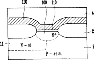
参看图3、图4A和图4B,在P-衬底的部分中形成N-阱11。通过元件隔离工艺限定场区和有源区后,利用氧化工艺在场区形成场氧化膜2。利用单元N+杂质离子注入工艺,在N-阱边缘的选择部分,形成单元间隔区100。在N-阱11中形成PMOS晶体管10,在P-衬底1中形成NMOS晶体管20。PMOS晶体管10包括公共栅极120,源和漏的第1和第2连接部分13A和13B,NMOS晶体管包括公共栅电极120。源和漏的第3和第4连接部分23A和23B。利用多晶硅淀积和构图工艺,形成公共栅电极120,以便互连PMOS晶体管10和NMOS晶体管20,并且越过单元间隔区100。在单元间隔区100和在其上面越过单元间隔区100的公共栅电极之间形成厚氧化膜110,该厚氧化膜110是在形成晶体管10和20形成工艺期间形成的。利用N+杂质离子注入工艺沿N-阱11边缘形成收集区3,并使收集区3和单元间隔区100相连。形成收集区3后,在结构上形成层间绝缘层4。以后,利用金属接触工艺由第1金属布线5A连接PMOS晶体管10的第1连接部分和NMOS晶体管20的第3连接部分23A,由第二金属布线5B把PMOS晶体管10的第2连接部分13B和NMOS晶体管20的第4连接部分23B连到其它部分。
如上所述,由于在形成栅电极工艺期间,PMOS晶体管的栅电极和NMOS晶体管的栅电极直接和多晶硅布线相连,不需要考虑金属接触工艺的裕虎所以可以进一步减少芯片的尺寸,由于在多晶硅布线下面的有源区形成单元间隔区,能防止寄生晶体管的形成。
如前所述,虽然叙述了优选的特殊实施例,那仅仅是为了说明本发明的原理。应该了解,本发明不限于上述公开和说明的优选实施例。因此,在本发明的范围和精神实质内所作的各种适当变化都包括在本发明的其它实施例中。
Claims (6)
1.一种制造CMOS晶体管的方法,包括下列步骤:
在形成N-阱的P-衬底中,限定场区和有源区;
在所述场区中形成场氧化膜;
在所述N-阱边缘选择部分形成单元隔离区;
在所述N-阱中,形成具有公共栅电极,第1连接部分和第2连接部分的PMOS晶体管,形成具有公共栅电极,第3连接部分和第4连接部分的NMOS晶体管;
沿所述N-阱边缘部分形成收集区;
形成所述收集区后在获得的结构上形成层间绝缘膜;
利用金属接触工艺,用第1金属布线连接所述第1连接部分和所述第3连接部分,用第2金属布线连接所述第2连接部分和所述第4连接部分。
2.按照权利要求1的方法,其特征是由多晶硅形成公共栅电极。
3.按照权利要求1的方法,其特征是,形成所述PMOS晶体管和NMOS晶体管的公共栅电极,其在上面越过所述单元隔离区。
4.按照权利要求1的方法,其特征是,在所述单元隔离区和公共栅电极之间形成厚氧化膜。
5.按照权利要求4的方法,其特征是,在形成晶体管所述栅氧化膜工艺期间,形成厚氧化膜。
6.按照权利要求1的方法,其特征是,在所述N-阱边缘连接所述单元隔离区和收集区。
Applications Claiming Priority (3)
| Application Number | Priority Date | Filing Date | Title |
|---|---|---|---|
| KR26537/1995 | 1995-08-25 | ||
| KR26537/95 | 1995-08-25 | ||
| KR1019950026537A KR0149256B1 (ko) | 1995-08-25 | 1995-08-25 | 씨모스 트랜지스터 제조방법 |
Publications (2)
| Publication Number | Publication Date |
|---|---|
| CN1149763A CN1149763A (zh) | 1997-05-14 |
| CN1058809C true CN1058809C (zh) | 2000-11-22 |
Family
ID=19424476
Family Applications (1)
| Application Number | Title | Priority Date | Filing Date |
|---|---|---|---|
| CN96113302A Expired - Fee Related CN1058809C (zh) | 1995-08-25 | 1996-08-25 | 制造cmos晶体管的方法 |
Country Status (5)
| Country | Link |
|---|---|
| US (1) | US5856215A (zh) |
| JP (1) | JPH09107038A (zh) |
| KR (1) | KR0149256B1 (zh) |
| CN (1) | CN1058809C (zh) |
| TW (1) | TW302526B (zh) |
Cited By (1)
| Publication number | Priority date | Publication date | Assignee | Title |
|---|---|---|---|---|
| CN101271900B (zh) * | 2007-02-17 | 2012-03-21 | 精工电子有限公司 | 半导体器件 |
Families Citing this family (4)
| Publication number | Priority date | Publication date | Assignee | Title |
|---|---|---|---|---|
| JPH11176949A (ja) * | 1997-12-15 | 1999-07-02 | Sony Corp | 半導体装置 |
| KR100424170B1 (ko) * | 2001-06-28 | 2004-03-24 | 주식회사 하이닉스반도체 | 반도체 소자의 풀 씨모스 에스램 셀 제조방법 |
| KR100464664B1 (ko) * | 2003-03-12 | 2005-01-03 | 주식회사 하이닉스반도체 | 고전압 소자의 웰 구조 |
| JP2008210902A (ja) * | 2007-02-24 | 2008-09-11 | Seiko Instruments Inc | カレントミラー回路 |
Citations (1)
| Publication number | Priority date | Publication date | Assignee | Title |
|---|---|---|---|---|
| EP0460833A1 (en) * | 1990-05-31 | 1991-12-11 | STMicroelectronics, Inc. | Field effect device with polycrystaline silicon channel |
Family Cites Families (12)
| Publication number | Priority date | Publication date | Assignee | Title |
|---|---|---|---|---|
| JPS57107066A (en) * | 1980-12-25 | 1982-07-03 | Toshiba Corp | Complementary semiconductor device and manufacture thereof |
| JPS5817655A (ja) * | 1981-07-24 | 1983-02-01 | Hitachi Ltd | 半導体装置の製造方法 |
| FR2555364B1 (fr) * | 1983-11-18 | 1990-02-02 | Hitachi Ltd | Procede de fabrication de connexions d'un dispositif a circuits integres a semi-conducteurs comportant en particulier un mitset |
| JPS61207052A (ja) * | 1985-03-12 | 1986-09-13 | Sanyo Electric Co Ltd | 高耐圧cmos半導体装置 |
| DE3650638T2 (de) * | 1985-03-22 | 1998-02-12 | Nec Corp | Integrierte Halbleiterschaltung mit Isolationszone |
| JPH01289157A (ja) * | 1988-05-17 | 1989-11-21 | Fujitsu Ltd | 相補型mosトランジスタとその製造方法 |
| JPH01308067A (ja) * | 1988-06-06 | 1989-12-12 | Nec Corp | 半導体装置 |
| JPH0252463A (ja) * | 1988-08-17 | 1990-02-22 | Texas Instr Japan Ltd | 半導体集積回路装置 |
| JPH0340463A (ja) * | 1989-03-15 | 1991-02-21 | Hitachi Ltd | 半導体装置及びその製造方法 |
| JPH0758701B2 (ja) * | 1989-06-08 | 1995-06-21 | 株式会社東芝 | 半導体装置の製造方法 |
| JP3184298B2 (ja) * | 1992-05-28 | 2001-07-09 | 沖電気工業株式会社 | Cmos出力回路 |
| US5506161A (en) * | 1994-10-24 | 1996-04-09 | Motorola, Inc. | Method of manufacturing graded channels underneath the gate electrode extensions |
-
1995
- 1995-08-25 KR KR1019950026537A patent/KR0149256B1/ko not_active IP Right Cessation
-
1996
- 1996-08-22 US US08/701,585 patent/US5856215A/en not_active Expired - Fee Related
- 1996-08-23 JP JP8221622A patent/JPH09107038A/ja active Pending
- 1996-08-23 TW TW085110288A patent/TW302526B/zh not_active IP Right Cessation
- 1996-08-25 CN CN96113302A patent/CN1058809C/zh not_active Expired - Fee Related
Patent Citations (1)
| Publication number | Priority date | Publication date | Assignee | Title |
|---|---|---|---|---|
| EP0460833A1 (en) * | 1990-05-31 | 1991-12-11 | STMicroelectronics, Inc. | Field effect device with polycrystaline silicon channel |
Cited By (1)
| Publication number | Priority date | Publication date | Assignee | Title |
|---|---|---|---|---|
| CN101271900B (zh) * | 2007-02-17 | 2012-03-21 | 精工电子有限公司 | 半导体器件 |
Also Published As
| Publication number | Publication date |
|---|---|
| CN1149763A (zh) | 1997-05-14 |
| JPH09107038A (ja) | 1997-04-22 |
| KR0149256B1 (ko) | 1998-10-01 |
| KR970013406A (ko) | 1997-03-29 |
| TW302526B (zh) | 1997-04-11 |
| US5856215A (en) | 1999-01-05 |
Similar Documents
| Publication | Publication Date | Title |
|---|---|---|
| US5106773A (en) | Programmable gate array and methods for its fabrication | |
| US5753550A (en) | Semiconductor integrated circuit device having switching MISFET and capacitor element and method of producing the same, including wiring therefor and method of producing such wiring | |
| DE4417150C2 (de) | Verfahren zur Herstellung einer Anordnung mit selbstverstärkenden dynamischen MOS-Transistorspeicherzellen | |
| US6015729A (en) | Integrated chip multilayer decoupling capcitors | |
| JPH07183302A (ja) | 金属層の形成及びボンディング方法 | |
| US4278989A (en) | Semiconductor device having cross wires | |
| KR930010088B1 (ko) | 반도체 기억장치와 그 제조방법 | |
| CN1058809C (zh) | 制造cmos晶体管的方法 | |
| US4975764A (en) | High density BiCMOS circuits and methods of making same | |
| EP0310797B1 (en) | Merged complementary bipolar and MOS means and method | |
| US5650346A (en) | Method of forming MOSFET devices with buried bitline capacitors | |
| US5936289A (en) | Semiconductor device | |
| US4570175A (en) | Three-dimensional semiconductor device with thin film monocrystalline member contacting substrate at a plurality of locations | |
| JPH0774326A (ja) | 半導体装置及びその製造方法 | |
| JP3775803B2 (ja) | 半導体集積回路装置およびその製造方法 | |
| US5895945A (en) | Single polysilicon neuron MOSFET | |
| JP2001526003A (ja) | Mosトランジスタを有する半導体装置 | |
| US6274921B1 (en) | Semiconductor integrated circuit including protective transistor protecting another transistor during processing | |
| US5773855A (en) | Microelectronic circuit including silicided field-effect transistor elements that bifunction as interconnects | |
| JPH08330440A (ja) | シリコン・オン・インシュレータ半導体装置 | |
| JP2544419B2 (ja) | 半導体集積回路装置及びその製造方法 | |
| US6544830B2 (en) | Method of manufacturing a semiconductor device with multiple emitter contact plugs | |
| US6396110B1 (en) | Semiconductor device with multiple emitter contact plugs | |
| KR100290471B1 (ko) | 씨모스소자및그제조방법 | |
| US6420746B1 (en) | Three device DRAM cell with integrated capacitor and local interconnect |
Legal Events
| Date | Code | Title | Description |
|---|---|---|---|
| C10 | Entry into substantive examination | ||
| SE01 | Entry into force of request for substantive examination | ||
| C06 | Publication | ||
| PB01 | Publication | ||
| C14 | Grant of patent or utility model | ||
| GR01 | Patent grant | ||
| C17 | Cessation of patent right | ||
| CF01 | Termination of patent right due to non-payment of annual fee |
Granted publication date: 20001122 Termination date: 20100825 |