CN104170082B - 系统级封装件及其制造方法 - Google Patents
系统级封装件及其制造方法 Download PDFInfo
- Publication number
- CN104170082B CN104170082B CN201380010431.XA CN201380010431A CN104170082B CN 104170082 B CN104170082 B CN 104170082B CN 201380010431 A CN201380010431 A CN 201380010431A CN 104170082 B CN104170082 B CN 104170082B
- Authority
- CN
- China
- Prior art keywords
- substrate
- package
- semiconductor chip
- laminate
- contact pad
- Prior art date
- Legal status (The legal status is an assumption and is not a legal conclusion. Google has not performed a legal analysis and makes no representation as to the accuracy of the status listed.)
- Active
Links
Images


Classifications
-
- H—ELECTRICITY
- H01—ELECTRIC ELEMENTS
- H01L—SEMICONDUCTOR DEVICES NOT COVERED BY CLASS H10
- H01L21/00—Processes or apparatus adapted for the manufacture or treatment of semiconductor or solid state devices or of parts thereof
- H01L21/02—Manufacture or treatment of semiconductor devices or of parts thereof
- H01L21/04—Manufacture or treatment of semiconductor devices or of parts thereof the devices having at least one potential-jump barrier or surface barrier, e.g. PN junction, depletion layer or carrier concentration layer
- H01L21/50—Assembly of semiconductor devices using processes or apparatus not provided for in a single one of the subgroups H01L21/06 - H01L21/326, e.g. sealing of a cap to a base of a container
-
- H—ELECTRICITY
- H01—ELECTRIC ELEMENTS
- H01L—SEMICONDUCTOR DEVICES NOT COVERED BY CLASS H10
- H01L23/00—Details of semiconductor or other solid state devices
- H01L23/48—Arrangements for conducting electric current to or from the solid state body in operation, e.g. leads, terminal arrangements ; Selection of materials therefor
-
- H—ELECTRICITY
- H01—ELECTRIC ELEMENTS
- H01L—SEMICONDUCTOR DEVICES NOT COVERED BY CLASS H10
- H01L23/00—Details of semiconductor or other solid state devices
- H01L23/52—Arrangements for conducting electric current within the device in operation from one component to another, i.e. interconnections, e.g. wires, lead frames
- H01L23/538—Arrangements for conducting electric current within the device in operation from one component to another, i.e. interconnections, e.g. wires, lead frames the interconnection structure between a plurality of semiconductor chips being formed on, or in, insulating substrates
- H01L23/5389—Arrangements for conducting electric current within the device in operation from one component to another, i.e. interconnections, e.g. wires, lead frames the interconnection structure between a plurality of semiconductor chips being formed on, or in, insulating substrates the chips being integrally enclosed by the interconnect and support structures
-
- H—ELECTRICITY
- H01—ELECTRIC ELEMENTS
- H01L—SEMICONDUCTOR DEVICES NOT COVERED BY CLASS H10
- H01L24/00—Arrangements for connecting or disconnecting semiconductor or solid-state bodies; Methods or apparatus related thereto
- H01L24/01—Means for bonding being attached to, or being formed on, the surface to be connected, e.g. chip-to-package, die-attach, "first-level" interconnects; Manufacturing methods related thereto
- H01L24/18—High density interconnect [HDI] connectors; Manufacturing methods related thereto
- H01L24/23—Structure, shape, material or disposition of the high density interconnect connectors after the connecting process
- H01L24/24—Structure, shape, material or disposition of the high density interconnect connectors after the connecting process of an individual high density interconnect connector
-
- H—ELECTRICITY
- H01—ELECTRIC ELEMENTS
- H01L—SEMICONDUCTOR DEVICES NOT COVERED BY CLASS H10
- H01L24/00—Arrangements for connecting or disconnecting semiconductor or solid-state bodies; Methods or apparatus related thereto
- H01L24/01—Means for bonding being attached to, or being formed on, the surface to be connected, e.g. chip-to-package, die-attach, "first-level" interconnects; Manufacturing methods related thereto
- H01L24/26—Layer connectors, e.g. plate connectors, solder or adhesive layers; Manufacturing methods related thereto
- H01L24/28—Structure, shape, material or disposition of the layer connectors prior to the connecting process
- H01L24/29—Structure, shape, material or disposition of the layer connectors prior to the connecting process of an individual layer connector
-
- H—ELECTRICITY
- H01—ELECTRIC ELEMENTS
- H01L—SEMICONDUCTOR DEVICES NOT COVERED BY CLASS H10
- H01L24/00—Arrangements for connecting or disconnecting semiconductor or solid-state bodies; Methods or apparatus related thereto
- H01L24/01—Means for bonding being attached to, or being formed on, the surface to be connected, e.g. chip-to-package, die-attach, "first-level" interconnects; Manufacturing methods related thereto
- H01L24/26—Layer connectors, e.g. plate connectors, solder or adhesive layers; Manufacturing methods related thereto
- H01L24/31—Structure, shape, material or disposition of the layer connectors after the connecting process
- H01L24/33—Structure, shape, material or disposition of the layer connectors after the connecting process of a plurality of layer connectors
-
- H—ELECTRICITY
- H01—ELECTRIC ELEMENTS
- H01L—SEMICONDUCTOR DEVICES NOT COVERED BY CLASS H10
- H01L24/00—Arrangements for connecting or disconnecting semiconductor or solid-state bodies; Methods or apparatus related thereto
- H01L24/80—Methods for connecting semiconductor or other solid state bodies using means for bonding being attached to, or being formed on, the surface to be connected
- H01L24/83—Methods for connecting semiconductor or other solid state bodies using means for bonding being attached to, or being formed on, the surface to be connected using a layer connector
-
- H—ELECTRICITY
- H01—ELECTRIC ELEMENTS
- H01L—SEMICONDUCTOR DEVICES NOT COVERED BY CLASS H10
- H01L2224/00—Indexing scheme for arrangements for connecting or disconnecting semiconductor or solid-state bodies and methods related thereto as covered by H01L24/00
- H01L2224/01—Means for bonding being attached to, or being formed on, the surface to be connected, e.g. chip-to-package, die-attach, "first-level" interconnects; Manufacturing methods related thereto
- H01L2224/02—Bonding areas; Manufacturing methods related thereto
- H01L2224/03—Manufacturing methods
- H01L2224/034—Manufacturing methods by blanket deposition of the material of the bonding area
- H01L2224/0346—Plating
-
- H—ELECTRICITY
- H01—ELECTRIC ELEMENTS
- H01L—SEMICONDUCTOR DEVICES NOT COVERED BY CLASS H10
- H01L2224/00—Indexing scheme for arrangements for connecting or disconnecting semiconductor or solid-state bodies and methods related thereto as covered by H01L24/00
- H01L2224/01—Means for bonding being attached to, or being formed on, the surface to be connected, e.g. chip-to-package, die-attach, "first-level" interconnects; Manufacturing methods related thereto
- H01L2224/02—Bonding areas; Manufacturing methods related thereto
- H01L2224/04—Structure, shape, material or disposition of the bonding areas prior to the connecting process
- H01L2224/04026—Bonding areas specifically adapted for layer connectors
-
- H—ELECTRICITY
- H01—ELECTRIC ELEMENTS
- H01L—SEMICONDUCTOR DEVICES NOT COVERED BY CLASS H10
- H01L2224/00—Indexing scheme for arrangements for connecting or disconnecting semiconductor or solid-state bodies and methods related thereto as covered by H01L24/00
- H01L2224/01—Means for bonding being attached to, or being formed on, the surface to be connected, e.g. chip-to-package, die-attach, "first-level" interconnects; Manufacturing methods related thereto
- H01L2224/02—Bonding areas; Manufacturing methods related thereto
- H01L2224/04—Structure, shape, material or disposition of the bonding areas prior to the connecting process
- H01L2224/04105—Bonding areas formed on an encapsulation of the semiconductor or solid-state body, e.g. bonding areas on chip-scale packages
-
- H—ELECTRICITY
- H01—ELECTRIC ELEMENTS
- H01L—SEMICONDUCTOR DEVICES NOT COVERED BY CLASS H10
- H01L2224/00—Indexing scheme for arrangements for connecting or disconnecting semiconductor or solid-state bodies and methods related thereto as covered by H01L24/00
- H01L2224/01—Means for bonding being attached to, or being formed on, the surface to be connected, e.g. chip-to-package, die-attach, "first-level" interconnects; Manufacturing methods related thereto
- H01L2224/02—Bonding areas; Manufacturing methods related thereto
- H01L2224/04—Structure, shape, material or disposition of the bonding areas prior to the connecting process
- H01L2224/05—Structure, shape, material or disposition of the bonding areas prior to the connecting process of an individual bonding area
- H01L2224/0554—External layer
- H01L2224/05599—Material
- H01L2224/056—Material with a principal constituent of the material being a metal or a metalloid, e.g. boron [B], silicon [Si], germanium [Ge], arsenic [As], antimony [Sb], tellurium [Te] and polonium [Po], and alloys thereof
- H01L2224/05638—Material with a principal constituent of the material being a metal or a metalloid, e.g. boron [B], silicon [Si], germanium [Ge], arsenic [As], antimony [Sb], tellurium [Te] and polonium [Po], and alloys thereof the principal constituent melting at a temperature of greater than or equal to 950°C and less than 1550°C
- H01L2224/05655—Nickel [Ni] as principal constituent
-
- H—ELECTRICITY
- H01—ELECTRIC ELEMENTS
- H01L—SEMICONDUCTOR DEVICES NOT COVERED BY CLASS H10
- H01L2224/00—Indexing scheme for arrangements for connecting or disconnecting semiconductor or solid-state bodies and methods related thereto as covered by H01L24/00
- H01L2224/01—Means for bonding being attached to, or being formed on, the surface to be connected, e.g. chip-to-package, die-attach, "first-level" interconnects; Manufacturing methods related thereto
- H01L2224/02—Bonding areas; Manufacturing methods related thereto
- H01L2224/04—Structure, shape, material or disposition of the bonding areas prior to the connecting process
- H01L2224/06—Structure, shape, material or disposition of the bonding areas prior to the connecting process of a plurality of bonding areas
- H01L2224/0601—Structure
- H01L2224/0603—Bonding areas having different sizes, e.g. different heights or widths
-
- H—ELECTRICITY
- H01—ELECTRIC ELEMENTS
- H01L—SEMICONDUCTOR DEVICES NOT COVERED BY CLASS H10
- H01L2224/00—Indexing scheme for arrangements for connecting or disconnecting semiconductor or solid-state bodies and methods related thereto as covered by H01L24/00
- H01L2224/01—Means for bonding being attached to, or being formed on, the surface to be connected, e.g. chip-to-package, die-attach, "first-level" interconnects; Manufacturing methods related thereto
- H01L2224/02—Bonding areas; Manufacturing methods related thereto
- H01L2224/04—Structure, shape, material or disposition of the bonding areas prior to the connecting process
- H01L2224/06—Structure, shape, material or disposition of the bonding areas prior to the connecting process of a plurality of bonding areas
- H01L2224/061—Disposition
- H01L2224/0618—Disposition being disposed on at least two different sides of the body, e.g. dual array
- H01L2224/06181—On opposite sides of the body
-
- H—ELECTRICITY
- H01—ELECTRIC ELEMENTS
- H01L—SEMICONDUCTOR DEVICES NOT COVERED BY CLASS H10
- H01L2224/00—Indexing scheme for arrangements for connecting or disconnecting semiconductor or solid-state bodies and methods related thereto as covered by H01L24/00
- H01L2224/01—Means for bonding being attached to, or being formed on, the surface to be connected, e.g. chip-to-package, die-attach, "first-level" interconnects; Manufacturing methods related thereto
- H01L2224/18—High density interconnect [HDI] connectors; Manufacturing methods related thereto
- H01L2224/23—Structure, shape, material or disposition of the high density interconnect connectors after the connecting process
- H01L2224/24—Structure, shape, material or disposition of the high density interconnect connectors after the connecting process of an individual high density interconnect connector
- H01L2224/241—Disposition
- H01L2224/24151—Connecting between a semiconductor or solid-state body and an item not being a semiconductor or solid-state body, e.g. chip-to-substrate, chip-to-passive
- H01L2224/24221—Connecting between a semiconductor or solid-state body and an item not being a semiconductor or solid-state body, e.g. chip-to-substrate, chip-to-passive the body and the item being stacked
- H01L2224/24225—Connecting between a semiconductor or solid-state body and an item not being a semiconductor or solid-state body, e.g. chip-to-substrate, chip-to-passive the body and the item being stacked the item being non-metallic, e.g. insulating substrate with or without metallisation
- H01L2224/24227—Connecting between a semiconductor or solid-state body and an item not being a semiconductor or solid-state body, e.g. chip-to-substrate, chip-to-passive the body and the item being stacked the item being non-metallic, e.g. insulating substrate with or without metallisation the HDI interconnect not connecting to the same level of the item at which the semiconductor or solid-state body is mounted, e.g. the semiconductor or solid-state body being mounted in a cavity or on a protrusion of the item
-
- H—ELECTRICITY
- H01—ELECTRIC ELEMENTS
- H01L—SEMICONDUCTOR DEVICES NOT COVERED BY CLASS H10
- H01L2224/00—Indexing scheme for arrangements for connecting or disconnecting semiconductor or solid-state bodies and methods related thereto as covered by H01L24/00
- H01L2224/01—Means for bonding being attached to, or being formed on, the surface to be connected, e.g. chip-to-package, die-attach, "first-level" interconnects; Manufacturing methods related thereto
- H01L2224/26—Layer connectors, e.g. plate connectors, solder or adhesive layers; Manufacturing methods related thereto
- H01L2224/28—Structure, shape, material or disposition of the layer connectors prior to the connecting process
- H01L2224/29—Structure, shape, material or disposition of the layer connectors prior to the connecting process of an individual layer connector
- H01L2224/29001—Core members of the layer connector
- H01L2224/29099—Material
- H01L2224/29198—Material with a principal constituent of the material being a combination of two or more materials in the form of a matrix with a filler, i.e. being a hybrid material, e.g. segmented structures, foams
- H01L2224/29298—Fillers
- H01L2224/29299—Base material
- H01L2224/293—Base material with a principal constituent of the material being a metal or a metalloid, e.g. boron [B], silicon [Si], germanium [Ge], arsenic [As], antimony [Sb], tellurium [Te] and polonium [Po], and alloys thereof
- H01L2224/29338—Base material with a principal constituent of the material being a metal or a metalloid, e.g. boron [B], silicon [Si], germanium [Ge], arsenic [As], antimony [Sb], tellurium [Te] and polonium [Po], and alloys thereof the principal constituent melting at a temperature of greater than or equal to 950°C and less than 1550°C
- H01L2224/29339—Silver [Ag] as principal constituent
-
- H—ELECTRICITY
- H01—ELECTRIC ELEMENTS
- H01L—SEMICONDUCTOR DEVICES NOT COVERED BY CLASS H10
- H01L2224/00—Indexing scheme for arrangements for connecting or disconnecting semiconductor or solid-state bodies and methods related thereto as covered by H01L24/00
- H01L2224/01—Means for bonding being attached to, or being formed on, the surface to be connected, e.g. chip-to-package, die-attach, "first-level" interconnects; Manufacturing methods related thereto
- H01L2224/26—Layer connectors, e.g. plate connectors, solder or adhesive layers; Manufacturing methods related thereto
- H01L2224/31—Structure, shape, material or disposition of the layer connectors after the connecting process
- H01L2224/32—Structure, shape, material or disposition of the layer connectors after the connecting process of an individual layer connector
- H01L2224/321—Disposition
- H01L2224/32135—Disposition the layer connector connecting between different semiconductor or solid-state bodies, i.e. chip-to-chip
- H01L2224/32145—Disposition the layer connector connecting between different semiconductor or solid-state bodies, i.e. chip-to-chip the bodies being stacked
-
- H—ELECTRICITY
- H01—ELECTRIC ELEMENTS
- H01L—SEMICONDUCTOR DEVICES NOT COVERED BY CLASS H10
- H01L2224/00—Indexing scheme for arrangements for connecting or disconnecting semiconductor or solid-state bodies and methods related thereto as covered by H01L24/00
- H01L2224/01—Means for bonding being attached to, or being formed on, the surface to be connected, e.g. chip-to-package, die-attach, "first-level" interconnects; Manufacturing methods related thereto
- H01L2224/26—Layer connectors, e.g. plate connectors, solder or adhesive layers; Manufacturing methods related thereto
- H01L2224/31—Structure, shape, material or disposition of the layer connectors after the connecting process
- H01L2224/32—Structure, shape, material or disposition of the layer connectors after the connecting process of an individual layer connector
- H01L2224/321—Disposition
- H01L2224/32151—Disposition the layer connector connecting between a semiconductor or solid-state body and an item not being a semiconductor or solid-state body, e.g. chip-to-substrate, chip-to-passive
- H01L2224/32221—Disposition the layer connector connecting between a semiconductor or solid-state body and an item not being a semiconductor or solid-state body, e.g. chip-to-substrate, chip-to-passive the body and the item being stacked
- H01L2224/32225—Disposition the layer connector connecting between a semiconductor or solid-state body and an item not being a semiconductor or solid-state body, e.g. chip-to-substrate, chip-to-passive the body and the item being stacked the item being non-metallic, e.g. insulating substrate with or without metallisation
-
- H—ELECTRICITY
- H01—ELECTRIC ELEMENTS
- H01L—SEMICONDUCTOR DEVICES NOT COVERED BY CLASS H10
- H01L2224/00—Indexing scheme for arrangements for connecting or disconnecting semiconductor or solid-state bodies and methods related thereto as covered by H01L24/00
- H01L2224/01—Means for bonding being attached to, or being formed on, the surface to be connected, e.g. chip-to-package, die-attach, "first-level" interconnects; Manufacturing methods related thereto
- H01L2224/26—Layer connectors, e.g. plate connectors, solder or adhesive layers; Manufacturing methods related thereto
- H01L2224/31—Structure, shape, material or disposition of the layer connectors after the connecting process
- H01L2224/33—Structure, shape, material or disposition of the layer connectors after the connecting process of a plurality of layer connectors
- H01L2224/331—Disposition
- H01L2224/3318—Disposition being disposed on at least two different sides of the body, e.g. dual array
- H01L2224/33181—On opposite sides of the body
-
- H—ELECTRICITY
- H01—ELECTRIC ELEMENTS
- H01L—SEMICONDUCTOR DEVICES NOT COVERED BY CLASS H10
- H01L2224/00—Indexing scheme for arrangements for connecting or disconnecting semiconductor or solid-state bodies and methods related thereto as covered by H01L24/00
- H01L2224/73—Means for bonding being of different types provided for in two or more of groups H01L2224/10, H01L2224/18, H01L2224/26, H01L2224/34, H01L2224/42, H01L2224/50, H01L2224/63, H01L2224/71
- H01L2224/732—Location after the connecting process
- H01L2224/73251—Location after the connecting process on different surfaces
- H01L2224/73267—Layer and HDI connectors
-
- H—ELECTRICITY
- H01—ELECTRIC ELEMENTS
- H01L—SEMICONDUCTOR DEVICES NOT COVERED BY CLASS H10
- H01L2224/00—Indexing scheme for arrangements for connecting or disconnecting semiconductor or solid-state bodies and methods related thereto as covered by H01L24/00
- H01L2224/80—Methods for connecting semiconductor or other solid state bodies using means for bonding being attached to, or being formed on, the surface to be connected
- H01L2224/83—Methods for connecting semiconductor or other solid state bodies using means for bonding being attached to, or being formed on, the surface to be connected using a layer connector
- H01L2224/8319—Arrangement of the layer connectors prior to mounting
- H01L2224/83192—Arrangement of the layer connectors prior to mounting wherein the layer connectors are disposed only on another item or body to be connected to the semiconductor or solid-state body
-
- H—ELECTRICITY
- H01—ELECTRIC ELEMENTS
- H01L—SEMICONDUCTOR DEVICES NOT COVERED BY CLASS H10
- H01L2224/00—Indexing scheme for arrangements for connecting or disconnecting semiconductor or solid-state bodies and methods related thereto as covered by H01L24/00
- H01L2224/80—Methods for connecting semiconductor or other solid state bodies using means for bonding being attached to, or being formed on, the surface to be connected
- H01L2224/83—Methods for connecting semiconductor or other solid state bodies using means for bonding being attached to, or being formed on, the surface to be connected using a layer connector
- H01L2224/8338—Bonding interfaces outside the semiconductor or solid-state body
- H01L2224/83399—Material
- H01L2224/834—Material with a principal constituent of the material being a metal or a metalloid, e.g. boron [B], silicon [Si], germanium [Ge], arsenic [As], antimony [Sb], tellurium [Te] and polonium [Po], and alloys thereof
- H01L2224/83438—Material with a principal constituent of the material being a metal or a metalloid, e.g. boron [B], silicon [Si], germanium [Ge], arsenic [As], antimony [Sb], tellurium [Te] and polonium [Po], and alloys thereof the principal constituent melting at a temperature of greater than or equal to 950°C and less than 1550°C
- H01L2224/83455—Nickel [Ni] as principal constituent
-
- H—ELECTRICITY
- H01—ELECTRIC ELEMENTS
- H01L—SEMICONDUCTOR DEVICES NOT COVERED BY CLASS H10
- H01L2224/00—Indexing scheme for arrangements for connecting or disconnecting semiconductor or solid-state bodies and methods related thereto as covered by H01L24/00
- H01L2224/80—Methods for connecting semiconductor or other solid state bodies using means for bonding being attached to, or being formed on, the surface to be connected
- H01L2224/83—Methods for connecting semiconductor or other solid state bodies using means for bonding being attached to, or being formed on, the surface to be connected using a layer connector
- H01L2224/838—Bonding techniques
- H01L2224/8384—Sintering
-
- H—ELECTRICITY
- H01—ELECTRIC ELEMENTS
- H01L—SEMICONDUCTOR DEVICES NOT COVERED BY CLASS H10
- H01L23/00—Details of semiconductor or other solid state devices
- H01L23/02—Containers; Seals
- H01L23/04—Containers; Seals characterised by the shape of the container or parts, e.g. caps, walls
- H01L23/043—Containers; Seals characterised by the shape of the container or parts, e.g. caps, walls the container being a hollow construction and having a conductive base as a mounting as well as a lead for the semiconductor body
- H01L23/051—Containers; Seals characterised by the shape of the container or parts, e.g. caps, walls the container being a hollow construction and having a conductive base as a mounting as well as a lead for the semiconductor body another lead being formed by a cover plate parallel to the base plate, e.g. sandwich type
-
- H—ELECTRICITY
- H01—ELECTRIC ELEMENTS
- H01L—SEMICONDUCTOR DEVICES NOT COVERED BY CLASS H10
- H01L24/00—Arrangements for connecting or disconnecting semiconductor or solid-state bodies; Methods or apparatus related thereto
- H01L24/01—Means for bonding being attached to, or being formed on, the surface to be connected, e.g. chip-to-package, die-attach, "first-level" interconnects; Manufacturing methods related thereto
- H01L24/26—Layer connectors, e.g. plate connectors, solder or adhesive layers; Manufacturing methods related thereto
- H01L24/31—Structure, shape, material or disposition of the layer connectors after the connecting process
- H01L24/32—Structure, shape, material or disposition of the layer connectors after the connecting process of an individual layer connector
-
- H—ELECTRICITY
- H01—ELECTRIC ELEMENTS
- H01L—SEMICONDUCTOR DEVICES NOT COVERED BY CLASS H10
- H01L24/00—Arrangements for connecting or disconnecting semiconductor or solid-state bodies; Methods or apparatus related thereto
- H01L24/73—Means for bonding being of different types provided for in two or more of groups H01L24/10, H01L24/18, H01L24/26, H01L24/34, H01L24/42, H01L24/50, H01L24/63, H01L24/71
-
- H—ELECTRICITY
- H01—ELECTRIC ELEMENTS
- H01L—SEMICONDUCTOR DEVICES NOT COVERED BY CLASS H10
- H01L25/00—Assemblies consisting of a plurality of individual semiconductor or other solid state devices ; Multistep manufacturing processes thereof
- H01L25/03—Assemblies consisting of a plurality of individual semiconductor or other solid state devices ; Multistep manufacturing processes thereof all the devices being of a type provided for in the same subgroup of groups H01L27/00 - H01L33/00, or in a single subclass of H10K, H10N, e.g. assemblies of rectifier diodes
- H01L25/04—Assemblies consisting of a plurality of individual semiconductor or other solid state devices ; Multistep manufacturing processes thereof all the devices being of a type provided for in the same subgroup of groups H01L27/00 - H01L33/00, or in a single subclass of H10K, H10N, e.g. assemblies of rectifier diodes the devices not having separate containers
- H01L25/07—Assemblies consisting of a plurality of individual semiconductor or other solid state devices ; Multistep manufacturing processes thereof all the devices being of a type provided for in the same subgroup of groups H01L27/00 - H01L33/00, or in a single subclass of H10K, H10N, e.g. assemblies of rectifier diodes the devices not having separate containers the devices being of a type provided for in group H01L29/00
- H01L25/071—Assemblies consisting of a plurality of individual semiconductor or other solid state devices ; Multistep manufacturing processes thereof all the devices being of a type provided for in the same subgroup of groups H01L27/00 - H01L33/00, or in a single subclass of H10K, H10N, e.g. assemblies of rectifier diodes the devices not having separate containers the devices being of a type provided for in group H01L29/00 the devices being arranged next and on each other, i.e. mixed assemblies
-
- H—ELECTRICITY
- H01—ELECTRIC ELEMENTS
- H01L—SEMICONDUCTOR DEVICES NOT COVERED BY CLASS H10
- H01L25/00—Assemblies consisting of a plurality of individual semiconductor or other solid state devices ; Multistep manufacturing processes thereof
- H01L25/03—Assemblies consisting of a plurality of individual semiconductor or other solid state devices ; Multistep manufacturing processes thereof all the devices being of a type provided for in the same subgroup of groups H01L27/00 - H01L33/00, or in a single subclass of H10K, H10N, e.g. assemblies of rectifier diodes
- H01L25/04—Assemblies consisting of a plurality of individual semiconductor or other solid state devices ; Multistep manufacturing processes thereof all the devices being of a type provided for in the same subgroup of groups H01L27/00 - H01L33/00, or in a single subclass of H10K, H10N, e.g. assemblies of rectifier diodes the devices not having separate containers
- H01L25/07—Assemblies consisting of a plurality of individual semiconductor or other solid state devices ; Multistep manufacturing processes thereof all the devices being of a type provided for in the same subgroup of groups H01L27/00 - H01L33/00, or in a single subclass of H10K, H10N, e.g. assemblies of rectifier diodes the devices not having separate containers the devices being of a type provided for in group H01L29/00
- H01L25/072—Assemblies consisting of a plurality of individual semiconductor or other solid state devices ; Multistep manufacturing processes thereof all the devices being of a type provided for in the same subgroup of groups H01L27/00 - H01L33/00, or in a single subclass of H10K, H10N, e.g. assemblies of rectifier diodes the devices not having separate containers the devices being of a type provided for in group H01L29/00 the devices being arranged next to each other
-
- H—ELECTRICITY
- H01—ELECTRIC ELEMENTS
- H01L—SEMICONDUCTOR DEVICES NOT COVERED BY CLASS H10
- H01L2924/00—Indexing scheme for arrangements or methods for connecting or disconnecting semiconductor or solid-state bodies as covered by H01L24/00
- H01L2924/10—Details of semiconductor or other solid state devices to be connected
- H01L2924/11—Device type
- H01L2924/13—Discrete devices, e.g. 3 terminal devices
- H01L2924/1304—Transistor
- H01L2924/1306—Field-effect transistor [FET]
- H01L2924/13091—Metal-Oxide-Semiconductor Field-Effect Transistor [MOSFET]
-
- H—ELECTRICITY
- H01—ELECTRIC ELEMENTS
- H01L—SEMICONDUCTOR DEVICES NOT COVERED BY CLASS H10
- H01L2924/00—Indexing scheme for arrangements or methods for connecting or disconnecting semiconductor or solid-state bodies as covered by H01L24/00
- H01L2924/15—Details of package parts other than the semiconductor or other solid state devices to be connected
- H01L2924/181—Encapsulation
-
- H—ELECTRICITY
- H01—ELECTRIC ELEMENTS
- H01L—SEMICONDUCTOR DEVICES NOT COVERED BY CLASS H10
- H01L2924/00—Indexing scheme for arrangements or methods for connecting or disconnecting semiconductor or solid-state bodies as covered by H01L24/00
- H01L2924/19—Details of hybrid assemblies other than the semiconductor or other solid state devices to be connected
- H01L2924/191—Disposition
- H01L2924/19101—Disposition of discrete passive components
- H01L2924/19105—Disposition of discrete passive components in a side-by-side arrangement on a common die mounting substrate
Landscapes
- Engineering & Computer Science (AREA)
- Computer Hardware Design (AREA)
- Microelectronics & Electronic Packaging (AREA)
- Power Engineering (AREA)
- Physics & Mathematics (AREA)
- Condensed Matter Physics & Semiconductors (AREA)
- General Physics & Mathematics (AREA)
- Manufacturing & Machinery (AREA)
- Cooling Or The Like Of Semiconductors Or Solid State Devices (AREA)
- Production Of Multi-Layered Print Wiring Board (AREA)
- Die Bonding (AREA)
- Combinations Of Printed Boards (AREA)
Abstract
提供一种系统级封装件及其制造方法。系统级封装件包括具有基板(4)设置在其内部的层合体。半导体芯片(2)嵌入到层合体中,并且半导体通过烧结的键合层键合到基板(4)的接触垫(6),其中烧结的键合层由烧结膏制成。基板和提供层合体的其它层的层合以及烧结膏的烧结可以在单一、共同的固化步骤中执行。
Description
技术领域
本发明的实施例涉及系统级封装件(SIP),其包括具有基板和设置在其中的半导体芯片的层合体。另外,其它实施例涉及制造系统级封装件的方法。
背景技术
对成本降低的小型电子系统的需求的不断增长要求可靠和经济有效的半导体封装件具有小的形状因素。对于便携式电子产品,更小的封装和更小的子系统封装已经成为主流。尺寸减小不再仅仅集中于封装表面区域,封装件的厚度和重量也应该减小。
满足不断增长的客户需求的其中一种方法被称为“系统级封装件”,它被开发以解决许多应用诸如计算和通信所面临的日渐增多的挑战。系统级封装件,例如购自德州仪器公司(美国德克萨斯州达拉斯市)MicroSlP(μSIP)的封装件,包括半导体芯片、控制器,例如在层合基板中。另外,有源和/或无源电子组件(诸如电感器)通过将它们设置在层合基板或层合体的上表面的顶部上而被包含在系统级封装件中。
然而,半导体芯片的键合仍然基于引线框,这意味着芯片是利用铜夹片键合到引线框,引线框馈出到封装件底侧。铜夹片需要占用封装件内的空间。因此,相对于组装工艺速度可以对空间进行改进。
发明内容
根据本发明的一方面,提供一种系统级封装件,其包括层合体,所述层合体包括设置在其中的基板。优选地,基板被预先压制。半导体芯片嵌入在层合体中,并且半导体芯片的至少一个接触区域通过烧结的键合层键合到基板的接触垫,所述键合层由烧结膏制成。
根据本发明的一方面,系统级封装件可以在联合(combined)的压制和烧结工艺中制造。换言之,热和压力均被施加到形成层合体的堆叠体(stack)上。压制步骤通常从印刷电路板的制造中得知,并且通常在约200℃范围的工艺温度下执行。有利地,并且根据本发明的一方面,可以确定这种压制步骤的工艺参数也适于执行烧结工艺。因此,提供联合的压制和烧结步骤。烧结膏的烧结发生并且在用于堆叠体的层合的同一工艺步骤内提供烧结的键合层。
根据本发明的另一方面,提供一种制造系统级封装件的方法。将烧结膏施加到基板的接触垫和/或半导体芯片的接触区域。优选地,烧结膏的施加通过膏印刷执行,并且烧结膏被施加到半导体芯片的接触区域或基板的接触垫的二者之一。半导体芯片的接触区域放置在基板的接触垫上。换言之,半导体芯片的接触区域和基板的接触垫相互叠合(register)。将基板和所放置的半导体芯片以及形成系统级封装件的层合体的其它层堆叠到一起。最后,对堆叠体执行联合压制和烧结步骤。在这种联合压制和烧结步骤期间,堆叠体的基板和其它层被层合以提供层合体。进一步,在联合压制和烧结步骤期间,烧结膏的烧结被执行以提供基板的接触垫与半导体芯片的接触区域之间的电连接。换言之,堆叠体的层合和电接触在共同的单一工艺步骤中执行。
在联合压制和烧结步骤期间,所述堆叠体可暴露于热和压力中,如同通常所知的印刷电路板的制造。进一步,所述方法可包括预先压制基板的步骤,并且在压制和烧结堆叠体之前将半导体芯片设置在所述预先压制的基板上。进一步地,烧结膏的部分预烧结可以在最后的压制和烧结步骤之前执行。
附图说明
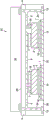
图1示出用于制造系统级封装件的简化堆叠体的示意图,示出了在放置半导体芯片之后并在烧结和压制堆叠体之前的堆叠,
图2示出图1的堆叠体的示意图,其中填充材料被插入后续基板之间,
图3示出通过固化从图1和图2得到的堆叠体来制造简化的系统级封装件的示意图,
图4示出图3的简化的系统级封装件的示意图,其中插入通孔以提供系统级封装件的上、中和下互联表面之间的连接,
图5示出没有下基板的进一步简化的系统级封装件的示意图,
图6示出没有与上表面和下表面相邻的基板的另一个简化的系统级封装件的示意图,
图7示出包括并排放置的两个功率场效应晶体管(FET)和堆叠在FET顶部的控制器的进一步简化的系统级封装件的示意图,
图8示出包括并排放置的两个功率FET和放置在上表面上的无源组件的另一个简化的系统级封装件的示意图,
图9示出包括并排放置的两个功率FET和无源组件的简化系统级封装件的示意图,其中芯片直接堆叠成芯片堆叠芯片的结构(die-on-die configuration),
图10和图11示出包括半导体芯片和提供高电流连接的金属块的进一步简化的系统级封装件的示意图。
具体实施方式
图1示出用于制造系统级封装件的一种简化堆叠体。示出了在放置半导体芯片2到各个基板4上之后并在烧结和压制堆叠体之前的堆叠。优选地,基板4被预先压制,并且进一步优选地,它们由印刷电路板材料诸如纤维增强树脂制成。基板4的接触垫6优选由铜制成,并具有由不活泼(noble)金属制成的镀层7。当考虑电势序时,镀层7的材料优选比铜更不活泼。优选地,采用镍银(NiAu)或镍金(NiAg)用于镀层7。有利地,例如,NiAu镀层7阻止铜(Cu)接触垫6在烧结过程中氧化。进一步地,存在设置在半导体芯片2的接触区域中的镀层7。半导体芯片2的前面和后面都可以提供有NiAu镀层7。换言之,每个接触区域或接触垫6(其被指定通过烧结的连接而进行耦合或接触)都提供有不活泼金属涂层7,以阻止烧结的电接触发生氧化。
导电通孔8(为了清晰起见,只有一些通孔8用附图标记标注)穿通基板4。对于设置在堆叠体中间的基板4,通孔8用于将设置在基板4的第一表面上的相应接触垫6与设置在基板4的相反表面上的另一接触垫6电耦合。优选地,导电通孔8是铜填充的钻孔。在上基板4处,通孔8将设置在基板4内表面处的接触垫6与设置在上表面28处的上接触垫10电耦合。类似的操作应用于下基板4,通孔8用于将设置在内表面处的接触垫6与设置在堆叠体的下表面26处的下接触垫12耦合。其它有源和/或无源组件可以设置在上表面28处,并且可以耦合到上接触垫12。如果系统级封装件安装到印刷电路板,则堆叠体的下表面26通常面朝印刷电路板。系统级封装到印刷电路板的电耦合可通过下接触垫12提供。
在图1的实施例中,基板4的接触垫6,更精确的是上基板和中间基板4的下接触垫6的镀层7设有烧结膏14,其优选通过烧结膏印刷施加。优选地,烧结膏14由比Cu更不活泼的金属或金属合金制成。这也是考虑了电势序并且优选材料为基于Ag的烧结膏14。对于系统级封装件的制造,将烧结膏14施加于半导体芯片2的接触区域和基板4的接触垫6中的任一个或两者。优选地,并且根据图1的实施例,将烧结膏14印刷到基板4的接触垫6。然后将半导体芯片2放置在基板4的相应接触垫6上的烧结膏14的顶部上,这表示半导体芯片2的接触区域与基板4的接触垫6叠合。
在图1的实施例中,半导体芯片2的背面已经设置有烧结膏,并且已执行预烧结步骤,以便将半导体芯片2的背面附接到基板4。在预烧结步骤中,烧结膏变成烧结的键合层16,其设置在芯片2的背面和基板4的上接触垫6之间。例如,半导体芯片2是功率MOSFET,并且示出的堆叠体用于提供堆叠的功率FET结构。
图2示出从图1得知的堆叠体,其中填充材料18插入在相邻基板层4之间。填充材料18在堆叠步骤期间被添加到堆叠体,并且优选地,填充材料18被预切割以适应半导体芯片2。填充材料18还可以适应附加的有源和/或无源组件(未示出),这些组件可以集成在系统级封装件中。填充材料18用于在后续压制和烧结步骤期间填充堆叠体中的空隙。
在联合压制和烧结步骤中,图2的堆叠体暴露于热和压力,其中执行该步骤的参数可以在通常从印刷电路板的制造中得知的温度和压力的范围中。例如,可采用约200℃的固化温度。在所述联合压制和烧结步骤期间,执行基板4和填充材料18的层合以提供系统级封装件的层合体。同时,对烧结膏14进行烧结,以便耦合或键合基板4的接触垫6和半导体芯片2的连接区域。有利地,系统级封装件可以在联合工艺步骤中制造,这意味着层合和烧结是在单一共同的工艺步骤中执行。这简化了系统级封装件的制造工艺。进一步有利的是,半导体芯片2直接键合到相应的导电路径或基板4的接触垫6。不需要引线框。引线框以及半导体芯片2与引线框之间所需的键合线的键合工艺的弃用对于制造成本是有利的,并且进一步加速制造过程。
图3示出包括层合体的简化的系统级封装件20,其中层合体基本上由基板4、固化的填充材料22和嵌入的半导体芯片2制成。在联合压制和烧结步骤中,先前已经施加或印刷在上基板和中间基板4的下接触垫6上的烧结膏垫16变成烧结的键合层16。半导体芯片2的接触区域通过烧结的键合层16耦合到基板4的接触垫6。
在图3的系统级封装件20中,半导体芯片2经由导电通孔8耦合到上接触垫10和下接触垫12。其它有源和/或无源电子组件可以嵌入在上接触垫10上或耦合到上接触垫10。例如,对于给定的堆叠的功率MOSFET结构,这些其它有源和/或无源电子组件(未示出)可以是电感器或电容器,以便提供具有较小形状因素和较小封装的高度集成的功率变换器。系统级封装件2的下接触垫12可通过采用任意常规键合或焊接技术耦合到电子设备的印刷电路板。
图4示出图3的系统级封装件20,然而,根据图4的实施例,垂直连接件24(其可以是铜填充的通孔)被插入到系统级封装件20中。如果需要,垂直连接件24用于将系统级封装件20的上接触垫10与下接触垫12和中间基板4的接触垫12耦合。系统级封装件20还可以包括电子组件(未示出),其嵌入到层合体中。例如,控制器可以集成到系统级封装件20中,并且可以用于控制功率MOSFET(即半导体芯片2),以便提供高度集成的功率级。这些其它有源和/或无源电子组件可通过垂直连接件24耦合到系统级封装件20的相应上和/或下接触垫10、12。优选地,其它电子组件,例如,控制器芯片或小电容器嵌入在系统级封装件20的第二层中。因此,上侧28的空间可被利用以用于模块所需的较大电子部件或组件。
根据本发明的另一个实施例,同一半导体芯片2的接触区域可经由基板4耦合。换言之,半导体芯片2的第一接触区域可耦合到基板4的接触垫6,并且所述基板4的另一个接触垫6耦合到所述半导体芯片2的另一个接触区域。根据本发明的一方面,另一个接触区域可以是另一个半导体芯片2的接触区域。后续实施例允许经由基板4耦合两个或更多个半导体芯片2。各个接触区域和接触垫6之间的电连接可由烧结膏14制成的烧结的键合层16提供。有利地,这一方面消除了复杂的芯片间引线键合的需要。可以简化各系统级封装件组装到的PCB的复杂布线。
尤其是当功率MOSFET被用作半导体芯片2时,半导体芯片2的热耦合会是重要的问题。因此,可以有利地提供这样的系统级封装件20,即不具有与系统级封装件20的上和/或下表面28、26相邻的基板层4。
图5示出根据本发明的一个实施例的另一个简化的系统级封装件20,其中基板4不与下表面26相邻。因此,尤其对于下部半导体芯片2,到印刷电路板具有非常高效的热传递,其中印刷电路板可以设置成相邻于系统级封装件20的下表面26。在原理上,图5中的系统级封装件20的结构从图4获知,除了没有基板4相邻于下表面26。因此,图5的系统级封装件20的结构将不再重复说明。
图6示出根据本发明的另一个实施例的另一步简化的系统级封装件20。为提供系统级封装件20的上部芯片2到上表面28以及下部芯片2到下表面26的高效热耦合,可以有利地分配与下表面26相邻的基板4,以及分配与上表面28相邻的基板4。因此,根据图6的实施例的系统级封装件20只包括位于系统级封装件20中心的单个基板4。这对于上部半导体芯片和下部半导体芯片而言,具有非常高效的散热。根据图6的实施例的系统级封装件20的结构在原理上从图5获知,除了省略与上表面28相邻的基板4。因此,对于系统级封装件20的结构的说明不再重复。
图7示出根据本发明的另一个实施例的简化的系统级封装件20。系统级封装件20包括基板层4,其设置在系统级封装件20的中心并且与嵌入第一和第二半导体芯片2的固化的填充材料22相邻,其中第一半导体芯片和第二半导体芯片以堆叠的方式设置在下层中。进一步地,控制器30设置在系统级封装件20的上层中。系统级封装件20的下表面26处没有基板层,以便提供从半导体芯片2(根据图7中的实施例,其为功率MOSFET)到印刷电路板的高效散热,其中所述印刷电路板可以与系统级封装件20的下侧26相邻。
半导体芯片2通过烧结的键合层16键合到嵌入于系统级封装件20的下表面26中的下接触垫12和基板4的接触垫6。类似的操作应用于控制器30,所述控制器30通过烧结的键合层16键合到基板层4。然而,也可以采用标准的芯片附接方法键合控制器30。如已经关于图1至图6中的实施例提到的,根据图7的实施例的系统级封装件20可以是层叠的,并且为提供半导体芯片2与控制器30的键合的层合体(主要包括基板4和填充材料,被示为固化的填充材料22)的层合以及烧结膏垫的烧结是在单个联合的工艺步骤中执行。可通过使用常规技术将用于耦合控制器30的其它接触件32插入系统级封装件20的上表面28中。控制器30到下接触垫12的耦合可通过垂直连接件24提供,其中所述垂直连接件24可以是铜填充的通孔并且用于将控制器30的上侧与下接触垫12耦合。上表面28顶部上的附加层能够提供用于上部设置的外部组件的空间和互连。
图8示出类似于根据图7的系统级封装件20的配置的简化的系统级封装件20。然而,基板4没有设置在堆叠体的中心。基板4设置成相邻于系统级封装件20的上表面28。利用常规技术将控制器30耦合于基板4的接触垫6。基板4的接触垫6到下接触垫12的耦合可通过垂直连接件24提供,其中所述垂直连接件24可以是铜填充的通孔。半导体芯片2和控制器30(半导体芯片2仍然可以是功率MOSFET)嵌入在固化的填充材料22中。半导体芯片2通过从图7得知的烧结的键合层16耦合到下接触垫12。然而,半导体芯片2和控制器30设置成芯片堆叠芯片的结构,这意味着芯片2和控制器30直接互相堆叠在其上,中间没有基板。芯片2、30的键合通过烧结的键合层16执行。控制器芯片30的背面(其镀有不活泼金属镀层7)相邻于烧结的键合层16,其进一步相邻于半导体芯片2的不活泼金属镀层7。
图9示出另一个简化的系统级封装件20,其包括两个半导体芯片2,其中所述两个半导体芯片2可以是半导体半桥结构的功率MOSFET。系统级封装件20包括基板4,其相邻于系统级封装件20的上表面28。基板4包括接触垫6,其通过烧结的键合层16耦合到半导体芯片2的接触区域。半导体芯片2的背面通过烧结的键合层16耦合到下接触垫12。有利地,可以提供从半导体芯片2到印刷电路板的高效散热,其中所述印刷电路板可以相邻于系统级封装件20的下表面26。设置在半导体芯片2的上部有源侧的半导体芯片2的接触区域还可以通过垂直连接件24耦合到下接触垫12,其中所述垂直连接件24延伸通过层合体向下到达基板层4的接触垫6。外部散热器(未示出)或其他有源和/或无源元件34可以附接到上表面28。仅示例,其他元件34通过垂直连接件24耦合到下接触垫12。进一步地,上表面28的顶部上可以存在额外基板层(未示出),其能够提供用于额外有源和/或无源外部组件的空间。
图10示出包括两个半导体芯片2的简化的系统级封装件20,其中所述两个半导体芯片可以是半导体半桥结构的功率MOSFET。进一步地,根据图10中的实施例的系统级封装件20包括金属块36,其用作高电流导电路径。其它有源和/或无源电子组件(未示出)可集成到系统级封装件20中。半导体芯片2通过烧结的键合层16耦合到基板4的接触垫6和下接触垫12,其中所述烧结的键合层16相邻于接触垫6、12的相应镀层7。金属块36的上表面和下表面也设有镀层7。优选地,将Cu块用作金属块36。为阻止Cu在烧结工艺期间发生氧化,金属块36上具有不活泼金属镀层7。Cu的氧化将有可能损坏烧结的键合的质量,但由于存在镀层7,因此可以不考虑这种现象。金属块36用作高电流连接件,提供从半导体芯片2的上侧经由接触垫6和金属块36到电路板的导电路径,其中所述电路板可设置成相邻于系统级封装件20的下表面。
通常,金属块36的集成与半导体芯片2的集成具有可比性。换言之,如果有必要或需要,上述引用的实施例中的每个半导体芯片2可以用适当电镀的金属块26替代。金属块36在系统级封装件20中的集成和设置可由高电流连接件的需求驱动。
图11示出另一个简化的系统级封装件20,其与根据图10的系统级封装件20具有可比性。为了清晰起见,仅示出单个半导体芯片2。然而,图11中的系统级封装件可以类似于图10中的实施例配置,这意味着系统级封装件可包括设置成半桥结构的两个半导体芯片2。在图11中,图11左侧的垂直连接件24由填充的通孔提供。然而,垂直连接件可由金属球36提供,其示出在系统级封装件20的右侧。金属球36包括不活泼金属镀层7,并且被烧结,经由烧结的键合层16一边到达接触垫6,另一边到达接触垫12。金属球36的嵌入可类似于金属块36的集成,金属块36被示出在系统级封装件20的中心。
尽管已在本文参考具体实施例描述了本发明,但并不限于这些实施例,并且毫无疑义的,本领域技术人员将想到落入要求保护的本发明的范围内的其它替代实施例。
Claims (11)
1.一种系统级封装件,所述系统级封装件具有:
层合体;
设置在所述层合体内部的基板;
所述基板上的至少一个接触垫;和
嵌入于所述层合体中的半导体芯片,
其中所述半导体芯片的至少一个接触区域通过烧结的键合层键合到所述基板的所述至少一个接触垫,其中所述半导体芯片的接触区域由金属或金属合金制成或镀有金属或金属合金,当考虑电势序时,所述金属或金属合金比铜更不活泼。
2.根据权利要求1所述的系统级封装件,其中所述半导体芯片的所述接触区域具有铜基和设置在所述铜基上的金属涂层,所述金属涂层包含银或金。
3.根据权利要求1所述的系统级封装件,其中所述基板的所述接触垫具有铜基和设置在所述铜基上的金属涂层,所述金属涂层包含银或金。
4.一种系统级封装件,所述系统级封装件具有:
层合体;
设置在所述层合体内部的基板;
所述基板上的至少一个接触垫;和
嵌入于所述层合体中的半导体芯片,
其中所述半导体芯片的至少一个接触区域通过烧结的键合层键合到所述基板的所述至少一个接触垫,其中所述基板的接触垫由金属或金属合金制成或镀有金属或金属合金,当考虑电势序时,所述金属或金属合金比铜更不活泼。
5.一种系统级封装件,所述系统级封装件具有:
层合体;
设置在所述层合体内部的基板;
所述基板上的至少一个接触垫;和
嵌入于所述层合体中的半导体芯片,
其中所述半导体芯片的至少一个接触区域通过烧结的键合层键合到所述基板的所述至少一个接触垫,其中,所述烧结的键合层由包括金属或金属合金的烧结膏制成,当考虑电势序时,所述金属或金属合金比铜更不活泼。
6.一种系统级封装件,所述系统级封装件具有:
层合体;
设置在所述层合体内部的基板;
所述基板上的至少一个接触垫;和
嵌入于所述层合体中的半导体芯片,
其中所述半导体芯片的至少一个接触区域通烧结的键合层键合到所述基板的所述至少一个接触垫,其中所述半导体芯片耦合到所述封装件的上接触垫和/或下接触垫,所述上接触垫和/或下接触垫设置在所述层合体的上表面或下表面,其中没有基板被设置成相邻于所述层合体的所述上表面和/或下表面。
7.一种系统级封装件,所述系统级封装件具有:
层合体;
设置在所述层合体内部的基板;
所述基板上的至少一个接触垫;和
嵌入于所述层合体中的半导体芯片,
其中所述半导体芯片的至少一个接触区域通过烧结的键合层键合到所述基板的所述至少一个接触垫,其中,多个半导体芯片嵌入所述层合体中,并且其中所述多个半导体芯片的接触区域通过烧结膏制成的烧结的键合层相互键合,并且其中所述多个半导体芯片直接堆叠成芯片堆叠芯片的结构,而不在所述芯片之间设置基板。
8.一种系统级封装件,所述系统级封装件具有:
层合体;
设置在所述层合体内部的第一基板;
所述第一基板上的至少一个接触垫;
嵌入于所述层合体中的半导体芯片,
其中所述半导体芯片的至少一个接触区域通过烧结的键合层键合到所述第一基板的所述至少一个接触垫;
设置在所述第一基板上的多个半导体芯片,其中第一半导体芯片和第二半导体芯片设置在所述第一基板的相对表面上,从而形成堆叠的半导体结构;
第二基板,其被设置成关于所述第一半导体芯片或第二半导体芯片与所述第一基板相对;和
第三基板,其被设置成关于所述第一基板与所述第二基板相对,以便形成具有分别设置在上表面和下表面上的所述第二基板和所述第三基板的封装件,并提供关于所述第一基板对称的堆叠封装件。
9.根据权利要求8所述的系统级封装件,进一步包括高导电性材料的金属块,当考虑电势序时,所述金属块具有由比铜更不活泼的金属或金属合金制成的涂层。
10.根据权利要求9所述的系统级封装件,其中所述金属块是铜块并且所述涂层包含银和/或金。
11.一种制造系统级封装件的方法,所述方法包括:
将第一基板嵌入于层合体中,
对所述第一基板的多个接触垫和/或第一半导体芯片的多个接触区域施加烧结膏,
将所述第一半导体芯片的所述接触区域放置在所述第一基板的所述接触垫上,
将所述第一基板和所放置的第一半导体芯片与形成所述系统级封装件的层合体的其它层堆叠到一起,其中所述其它层包括:
至少第二半导体芯片,其设置在所述第一基板的相对表面上,从而形成堆叠的半导体结构;
第二基板,其被设置成关于所述第一半导体芯片或第二半导体芯片与所述第一基板相对;
第三基板,其被设置成关于所述第一基板与所述第二基板相对,以便形成具有分别设置在上表面和下表面上的所述第二基板和所述第三基板的封装件,并提供关于所述第一基板对称的堆叠封装件;以及
对所述堆叠执行联合的压制和烧结步骤,以便层合所述第一基板和所述其它层,从而提供所述层合体并执行所述烧结膏的烧结以提供所述接触垫与所述接触区域之间的电连接,其中,在所述联合的压制和烧结步骤中提供层合和电接触。
Applications Claiming Priority (5)
| Application Number | Priority Date | Filing Date | Title |
|---|---|---|---|
| EP12156909 | 2012-02-24 | ||
| EP12156909.9 | 2012-02-24 | ||
| US13/770,237 | 2013-02-19 | ||
| US13/770,237 US8884343B2 (en) | 2012-02-24 | 2013-02-19 | System in package and method for manufacturing the same |
| PCT/US2013/027656 WO2013126893A1 (en) | 2012-02-24 | 2013-02-25 | System in package and method for manufacturing the same |
Publications (2)
| Publication Number | Publication Date |
|---|---|
| CN104170082A CN104170082A (zh) | 2014-11-26 |
| CN104170082B true CN104170082B (zh) | 2021-09-03 |
Family
ID=49001956
Family Applications (1)
| Application Number | Title | Priority Date | Filing Date |
|---|---|---|---|
| CN201380010431.XA Active CN104170082B (zh) | 2012-02-24 | 2013-02-25 | 系统级封装件及其制造方法 |
Country Status (4)
| Country | Link |
|---|---|
| US (1) | US8884343B2 (zh) |
| JP (3) | JP6384868B2 (zh) |
| CN (1) | CN104170082B (zh) |
| WO (1) | WO2013126893A1 (zh) |
Families Citing this family (33)
| Publication number | Priority date | Publication date | Assignee | Title |
|---|---|---|---|---|
| US8884343B2 (en) * | 2012-02-24 | 2014-11-11 | Texas Instruments Incorporated | System in package and method for manufacturing the same |
| US9294046B2 (en) | 2013-03-15 | 2016-03-22 | Rf Micro Devices (Cayman Islands), Ltd. | RF power amplifier with PM feedback linearization |
| US9899133B2 (en) | 2013-08-01 | 2018-02-20 | Qorvo Us, Inc. | Advanced 3D inductor structures with confined magnetic field |
| US9705478B2 (en) | 2013-08-01 | 2017-07-11 | Qorvo Us, Inc. | Weakly coupled tunable RF receiver architecture |
| WO2015049944A1 (ja) * | 2013-10-03 | 2015-04-09 | 富士電機株式会社 | 半導体モジュール |
| US10242969B2 (en) | 2013-11-12 | 2019-03-26 | Infineon Technologies Ag | Semiconductor package comprising a transistor chip module and a driver chip module and a method for fabricating the same |
| US9437516B2 (en) * | 2014-01-07 | 2016-09-06 | Infineon Technologies Austria Ag | Chip-embedded packages with backside die connection |
| US10104764B2 (en) * | 2014-03-18 | 2018-10-16 | Texas Instruments Incorporated | Electronic device package with vertically integrated capacitors |
| US10257937B2 (en) * | 2014-07-07 | 2019-04-09 | Infineon Technologies Austria Ag | Device for electrically coupling a plurality of semiconductor device layers by a common conductive layer |
| EP2988328B1 (en) * | 2014-08-19 | 2021-05-12 | ABB Schweiz AG | Power semiconductor module and method of manufacturing the same |
| JP6500563B2 (ja) * | 2015-03-31 | 2019-04-17 | アイシン・エィ・ダブリュ株式会社 | スイッチング素子ユニット |
| SG10201504273UA (en) * | 2015-05-29 | 2016-12-29 | Delta Electronics Int’L Singapore Pte Ltd | Power module |
| KR102394542B1 (ko) * | 2015-07-30 | 2022-05-04 | 현대자동차 주식회사 | 반도체 패키지 및 그 제조 방법 |
| US10796835B2 (en) * | 2015-08-24 | 2020-10-06 | Qorvo Us, Inc. | Stacked laminate inductors for high module volume utilization and performance-cost-size-processing-time tradeoff |
| ITUB20153344A1 (it) * | 2015-09-02 | 2017-03-02 | St Microelectronics Srl | Modulo di potenza elettronico con migliorata dissipazione termica e relativo metodo di fabbricazione |
| FR3041210B1 (fr) * | 2015-09-15 | 2017-09-15 | Sagem Defense Securite | Procede d'assemblage par frittage d'argent sans pression |
| CN105261611B (zh) * | 2015-10-15 | 2018-06-26 | 矽力杰半导体技术(杭州)有限公司 | 芯片的叠层封装结构及叠层封装方法 |
| US10707171B2 (en) * | 2015-12-22 | 2020-07-07 | Intel Corporation | Ultra small molded module integrated with die by module-on-wafer assembly |
| US10845375B2 (en) * | 2016-02-19 | 2020-11-24 | Agjunction Llc | Thermal stabilization of inertial measurement units |
| DE102016108000B3 (de) * | 2016-04-29 | 2016-12-15 | Danfoss Silicon Power Gmbh | Verfahren zum stoffschlüssigen Verbinden einer ersten Komponente eines Leistungshalbleitermoduls mit einer zweiten Komponente eines Leistungshalbleitermoduls |
| US9824976B1 (en) * | 2016-08-16 | 2017-11-21 | Infineon Technologies Americas Corp. | Single-sided power device package |
| US11139238B2 (en) | 2016-12-07 | 2021-10-05 | Qorvo Us, Inc. | High Q factor inductor structure |
| FR3060243B1 (fr) * | 2016-12-12 | 2019-08-23 | Institut Vedecom | Module de commutation de puissance, convertisseur integrant celui-ci et procede de fabrication |
| EP3584833B1 (en) * | 2018-06-19 | 2021-09-01 | Mitsubishi Electric R&D Centre Europe B.V. | Power module with improved alignment |
| US20200176355A1 (en) * | 2018-12-04 | 2020-06-04 | Intel Corporation | Substrate embedded heat pipe |
| WO2021077354A1 (zh) | 2019-10-24 | 2021-04-29 | 京东方科技集团股份有限公司 | 驱动基板及其制作方法、显示装置 |
| DE102020106518A1 (de) | 2020-03-10 | 2021-09-16 | Infineon Technologies Ag | Halbleitervorrichtungen mit parallelen elektrisch leitenden Schichten |
| JP7475925B2 (ja) | 2020-03-31 | 2024-04-30 | 愛三工業株式会社 | 電子基板 |
| DE102020211631A1 (de) | 2020-09-17 | 2022-03-17 | Robert Bosch Gesellschaft mit beschränkter Haftung | Halbleitermodul für einen schweisstransformator und verfahren zum herstellen eines solchen halbleitermoduls |
| EP4016618A1 (en) | 2020-12-21 | 2022-06-22 | Hamilton Sundstrand Corporation | Power device packaging |
| DE102021109658B3 (de) | 2021-04-16 | 2022-10-20 | Danfoss Silicon Power Gmbh | Verfahren zur Herstellung eines Halbleiter-Leistungsgeräts und damit hergestelltes Halbleiter-Leistungsgerät sowie ein Werkzeugteil für eine Sinterpresse und Verwendung einer Sinterpresse |
| DE102021109666B3 (de) | 2021-04-16 | 2022-10-20 | Danfoss Silicon Power Gmbh | Elektronisches Gerät und Verfahren zu dessen Herstellung |
| WO2023175675A1 (ja) * | 2022-03-14 | 2023-09-21 | 三菱電機株式会社 | パワーモジュール半導体パッケージおよび半導体装置 |
Citations (3)
| Publication number | Priority date | Publication date | Assignee | Title |
|---|---|---|---|---|
| CN1428851A (zh) * | 2001-12-25 | 2003-07-09 | 譁裕实业股份有限公司 | 基片或芯片输入输出接点上金属凸块结构及其制造方法 |
| CN102097427A (zh) * | 2009-11-10 | 2011-06-15 | 英飞凌科技股份有限公司 | 层叠型电子器件 |
| CN102215639A (zh) * | 2010-04-02 | 2011-10-12 | 株式会社电装 | 半导体芯片内置配线基板及其制造方法 |
Family Cites Families (14)
| Publication number | Priority date | Publication date | Assignee | Title |
|---|---|---|---|---|
| JP2000151112A (ja) | 1998-11-10 | 2000-05-30 | Toshiba Corp | 配線基板及びその製造方法 |
| JP2001044606A (ja) | 1999-08-02 | 2001-02-16 | Hitachi Ltd | 半導体パッケージの実装構造体およびその実装方法並びにそのリワーク方法 |
| JP2003197849A (ja) | 2001-10-18 | 2003-07-11 | Matsushita Electric Ind Co Ltd | 部品内蔵モジュールとその製造方法 |
| JP2006202938A (ja) * | 2005-01-20 | 2006-08-03 | Kojiro Kobayashi | 半導体装置及びその製造方法 |
| TWI352406B (en) * | 2006-11-16 | 2011-11-11 | Nan Ya Printed Circuit Board Corp | Embedded chip package with improved heat dissipati |
| JP2008153470A (ja) * | 2006-12-18 | 2008-07-03 | Renesas Technology Corp | 半導体装置および半導体装置の製造方法 |
| JP5151150B2 (ja) * | 2006-12-28 | 2013-02-27 | 株式会社日立製作所 | 導電性焼結層形成用組成物、これを用いた導電性被膜形成法および接合法 |
| US8350382B2 (en) * | 2007-09-21 | 2013-01-08 | Infineon Technologies Ag | Semiconductor device including electronic component coupled to a backside of a chip |
| WO2009150875A1 (ja) * | 2008-06-12 | 2009-12-17 | 株式会社安川電機 | パワーモジュールおよびその制御方法 |
| JP2010050189A (ja) * | 2008-08-20 | 2010-03-04 | Hitachi Metals Ltd | 接合材、半導体装置およびその製造方法 |
| US7898083B2 (en) * | 2008-12-17 | 2011-03-01 | Texas Instruments Incorporated | Method for low stress flip-chip assembly of fine-pitch semiconductor devices |
| US8193040B2 (en) | 2010-02-08 | 2012-06-05 | Infineon Technologies Ag | Manufacturing of a device including a semiconductor chip |
| JP2011238779A (ja) * | 2010-05-11 | 2011-11-24 | Mitsubishi Electric Corp | 導電性接合構造体、これを用いた半導体装置および半導体装置の製造方法 |
| US8884343B2 (en) * | 2012-02-24 | 2014-11-11 | Texas Instruments Incorporated | System in package and method for manufacturing the same |
-
2013
- 2013-02-19 US US13/770,237 patent/US8884343B2/en active Active
- 2013-02-25 JP JP2014558928A patent/JP6384868B2/ja active Active
- 2013-02-25 CN CN201380010431.XA patent/CN104170082B/zh active Active
- 2013-02-25 WO PCT/US2013/027656 patent/WO2013126893A1/en active Application Filing
-
2018
- 2018-07-20 JP JP2018136615A patent/JP6615284B2/ja active Active
-
2019
- 2019-10-10 JP JP2019186475A patent/JP7132467B2/ja active Active
Patent Citations (3)
| Publication number | Priority date | Publication date | Assignee | Title |
|---|---|---|---|---|
| CN1428851A (zh) * | 2001-12-25 | 2003-07-09 | 譁裕实业股份有限公司 | 基片或芯片输入输出接点上金属凸块结构及其制造方法 |
| CN102097427A (zh) * | 2009-11-10 | 2011-06-15 | 英飞凌科技股份有限公司 | 层叠型电子器件 |
| CN102215639A (zh) * | 2010-04-02 | 2011-10-12 | 株式会社电装 | 半导体芯片内置配线基板及其制造方法 |
Also Published As
| Publication number | Publication date |
|---|---|
| JP2015508244A (ja) | 2015-03-16 |
| CN104170082A (zh) | 2014-11-26 |
| JP6615284B2 (ja) | 2019-12-04 |
| US8884343B2 (en) | 2014-11-11 |
| JP2018190999A (ja) | 2018-11-29 |
| JP6384868B2 (ja) | 2018-09-05 |
| US20130221526A1 (en) | 2013-08-29 |
| JP2020021951A (ja) | 2020-02-06 |
| WO2013126893A1 (en) | 2013-08-29 |
| JP7132467B2 (ja) | 2022-09-07 |
Similar Documents
| Publication | Publication Date | Title |
|---|---|---|
| CN104170082B (zh) | 系统级封装件及其制造方法 | |
| US11605609B2 (en) | Ultra-thin embedded semiconductor device package and method of manufacturing thereof | |
| US10186477B2 (en) | Power overlay structure and method of making same | |
| US9704788B2 (en) | Power overlay structure and method of making same | |
| US9437516B2 (en) | Chip-embedded packages with backside die connection | |
| JP2012238874A (ja) | 組み込まれた電気部品を備える多層プリント回路基板構造およびそれを製造するための方法 | |
| CN110517991B (zh) | 金属陶瓷模块及其制造方法、电路板模块及其制造方法 | |
| US10096562B2 (en) | Power module package | |
| JPH10294423A (ja) | 半導体装置 | |
| CN102437140A (zh) | 具有烧结的金属连接的功率半导体模块及制造方法 | |
| KR100335454B1 (ko) | 반도체칩 모듈용 다층 회로기판 및 그의 제조방법 | |
| CN112447534B (zh) | 封装体及其制备方法 | |
| CN111668196A (zh) | 半导体封装件以及相关方法 | |
| JP2012074497A (ja) | 回路基板 | |
| WO2012116157A2 (en) | Chip module embedded in pcb substrate | |
| KR100628418B1 (ko) | 반도체 장치 및 반도체 장치의 제조 방법 | |
| CN112714539A (zh) | 电子组件及制造电子组件的方法 | |
| JP2011222554A (ja) | 半導体チップ内蔵配線基板 | |
| JP2005167159A (ja) | 積層型半導体装置 | |
| TWI286456B (en) | Multi-layer circuit board integrated with electronic elements and method for fabricating the same | |
| JP2004214464A (ja) | 半導体装置用パッケージ、その製造方法および半導体装置 | |
| WO2016176283A1 (en) | Sinter bearing leads |
Legal Events
| Date | Code | Title | Description |
|---|---|---|---|
| C06 | Publication | ||
| PB01 | Publication | ||
| C10 | Entry into substantive examination | ||
| SE01 | Entry into force of request for substantive examination | ||
| GR01 | Patent grant | ||
| GR01 | Patent grant |