EP3584833B1 - Power module with improved alignment - Google Patents
Power module with improved alignment Download PDFInfo
- Publication number
- EP3584833B1 EP3584833B1 EP18305763.7A EP18305763A EP3584833B1 EP 3584833 B1 EP3584833 B1 EP 3584833B1 EP 18305763 A EP18305763 A EP 18305763A EP 3584833 B1 EP3584833 B1 EP 3584833B1
- Authority
- EP
- European Patent Office
- Prior art keywords
- power
- conductive material
- electrical
- electrically conductive
- layer
- Prior art date
- Legal status (The legal status is an assumption and is not a legal conclusion. Google has not performed a legal analysis and makes no representation as to the accuracy of the status listed.)
- Active
Links
Images


Classifications
-
- H—ELECTRICITY
- H01—ELECTRIC ELEMENTS
- H01L—SEMICONDUCTOR DEVICES NOT COVERED BY CLASS H10
- H01L23/00—Details of semiconductor or other solid state devices
- H01L23/52—Arrangements for conducting electric current within the device in operation from one component to another, i.e. interconnections, e.g. wires, lead frames
- H01L23/538—Arrangements for conducting electric current within the device in operation from one component to another, i.e. interconnections, e.g. wires, lead frames the interconnection structure between a plurality of semiconductor chips being formed on, or in, insulating substrates
- H01L23/5389—Arrangements for conducting electric current within the device in operation from one component to another, i.e. interconnections, e.g. wires, lead frames the interconnection structure between a plurality of semiconductor chips being formed on, or in, insulating substrates the chips being integrally enclosed by the interconnect and support structures
-
- H—ELECTRICITY
- H01—ELECTRIC ELEMENTS
- H01L—SEMICONDUCTOR DEVICES NOT COVERED BY CLASS H10
- H01L21/00—Processes or apparatus adapted for the manufacture or treatment of semiconductor or solid state devices or of parts thereof
- H01L21/02—Manufacture or treatment of semiconductor devices or of parts thereof
- H01L21/04—Manufacture or treatment of semiconductor devices or of parts thereof the devices having at least one potential-jump barrier or surface barrier, e.g. PN junction, depletion layer or carrier concentration layer
- H01L21/48—Manufacture or treatment of parts, e.g. containers, prior to assembly of the devices, using processes not provided for in a single one of the subgroups H01L21/06 - H01L21/326
- H01L21/4814—Conductive parts
- H01L21/4846—Leads on or in insulating or insulated substrates, e.g. metallisation
-
- H—ELECTRICITY
- H01—ELECTRIC ELEMENTS
- H01L—SEMICONDUCTOR DEVICES NOT COVERED BY CLASS H10
- H01L23/00—Details of semiconductor or other solid state devices
- H01L23/48—Arrangements for conducting electric current to or from the solid state body in operation, e.g. leads, terminal arrangements ; Selection of materials therefor
- H01L23/488—Arrangements for conducting electric current to or from the solid state body in operation, e.g. leads, terminal arrangements ; Selection of materials therefor consisting of soldered or bonded constructions
- H01L23/498—Leads, i.e. metallisations or lead-frames on insulating substrates, e.g. chip carriers
- H01L23/49833—Leads, i.e. metallisations or lead-frames on insulating substrates, e.g. chip carriers the chip support structure consisting of a plurality of insulating substrates
-
- H—ELECTRICITY
- H01—ELECTRIC ELEMENTS
- H01L—SEMICONDUCTOR DEVICES NOT COVERED BY CLASS H10
- H01L24/00—Arrangements for connecting or disconnecting semiconductor or solid-state bodies; Methods or apparatus related thereto
- H01L24/01—Means for bonding being attached to, or being formed on, the surface to be connected, e.g. chip-to-package, die-attach, "first-level" interconnects; Manufacturing methods related thereto
- H01L24/18—High density interconnect [HDI] connectors; Manufacturing methods related thereto
- H01L24/19—Manufacturing methods of high density interconnect preforms
-
- H—ELECTRICITY
- H01—ELECTRIC ELEMENTS
- H01L—SEMICONDUCTOR DEVICES NOT COVERED BY CLASS H10
- H01L24/00—Arrangements for connecting or disconnecting semiconductor or solid-state bodies; Methods or apparatus related thereto
- H01L24/01—Means for bonding being attached to, or being formed on, the surface to be connected, e.g. chip-to-package, die-attach, "first-level" interconnects; Manufacturing methods related thereto
- H01L24/18—High density interconnect [HDI] connectors; Manufacturing methods related thereto
- H01L24/20—Structure, shape, material or disposition of high density interconnect preforms
-
- H—ELECTRICITY
- H01—ELECTRIC ELEMENTS
- H01L—SEMICONDUCTOR DEVICES NOT COVERED BY CLASS H10
- H01L24/00—Arrangements for connecting or disconnecting semiconductor or solid-state bodies; Methods or apparatus related thereto
- H01L24/01—Means for bonding being attached to, or being formed on, the surface to be connected, e.g. chip-to-package, die-attach, "first-level" interconnects; Manufacturing methods related thereto
- H01L24/42—Wire connectors; Manufacturing methods related thereto
- H01L24/47—Structure, shape, material or disposition of the wire connectors after the connecting process
- H01L24/48—Structure, shape, material or disposition of the wire connectors after the connecting process of an individual wire connector
-
- H—ELECTRICITY
- H01—ELECTRIC ELEMENTS
- H01L—SEMICONDUCTOR DEVICES NOT COVERED BY CLASS H10
- H01L24/00—Arrangements for connecting or disconnecting semiconductor or solid-state bodies; Methods or apparatus related thereto
- H01L24/93—Batch processes
- H01L24/95—Batch processes at chip-level, i.e. with connecting carried out on a plurality of singulated devices, i.e. on diced chips
- H01L24/96—Batch processes at chip-level, i.e. with connecting carried out on a plurality of singulated devices, i.e. on diced chips the devices being encapsulated in a common layer, e.g. neo-wafer or pseudo-wafer, said common layer being separable into individual assemblies after connecting
-
- H—ELECTRICITY
- H01—ELECTRIC ELEMENTS
- H01L—SEMICONDUCTOR DEVICES NOT COVERED BY CLASS H10
- H01L25/00—Assemblies consisting of a plurality of individual semiconductor or other solid state devices ; Multistep manufacturing processes thereof
- H01L25/03—Assemblies consisting of a plurality of individual semiconductor or other solid state devices ; Multistep manufacturing processes thereof all the devices being of a type provided for in the same subgroup of groups H01L27/00 - H01L33/00, or in a single subclass of H10K, H10N, e.g. assemblies of rectifier diodes
- H01L25/04—Assemblies consisting of a plurality of individual semiconductor or other solid state devices ; Multistep manufacturing processes thereof all the devices being of a type provided for in the same subgroup of groups H01L27/00 - H01L33/00, or in a single subclass of H10K, H10N, e.g. assemblies of rectifier diodes the devices not having separate containers
- H01L25/07—Assemblies consisting of a plurality of individual semiconductor or other solid state devices ; Multistep manufacturing processes thereof all the devices being of a type provided for in the same subgroup of groups H01L27/00 - H01L33/00, or in a single subclass of H10K, H10N, e.g. assemblies of rectifier diodes the devices not having separate containers the devices being of a type provided for in group H01L29/00
- H01L25/072—Assemblies consisting of a plurality of individual semiconductor or other solid state devices ; Multistep manufacturing processes thereof all the devices being of a type provided for in the same subgroup of groups H01L27/00 - H01L33/00, or in a single subclass of H10K, H10N, e.g. assemblies of rectifier diodes the devices not having separate containers the devices being of a type provided for in group H01L29/00 the devices being arranged next to each other
-
- H—ELECTRICITY
- H01—ELECTRIC ELEMENTS
- H01L—SEMICONDUCTOR DEVICES NOT COVERED BY CLASS H10
- H01L2224/00—Indexing scheme for arrangements for connecting or disconnecting semiconductor or solid-state bodies and methods related thereto as covered by H01L24/00
- H01L2224/01—Means for bonding being attached to, or being formed on, the surface to be connected, e.g. chip-to-package, die-attach, "first-level" interconnects; Manufacturing methods related thereto
- H01L2224/02—Bonding areas; Manufacturing methods related thereto
- H01L2224/04—Structure, shape, material or disposition of the bonding areas prior to the connecting process
- H01L2224/04105—Bonding areas formed on an encapsulation of the semiconductor or solid-state body, e.g. bonding areas on chip-scale packages
-
- H—ELECTRICITY
- H01—ELECTRIC ELEMENTS
- H01L—SEMICONDUCTOR DEVICES NOT COVERED BY CLASS H10
- H01L2224/00—Indexing scheme for arrangements for connecting or disconnecting semiconductor or solid-state bodies and methods related thereto as covered by H01L24/00
- H01L2224/01—Means for bonding being attached to, or being formed on, the surface to be connected, e.g. chip-to-package, die-attach, "first-level" interconnects; Manufacturing methods related thereto
- H01L2224/02—Bonding areas; Manufacturing methods related thereto
- H01L2224/04—Structure, shape, material or disposition of the bonding areas prior to the connecting process
- H01L2224/06—Structure, shape, material or disposition of the bonding areas prior to the connecting process of a plurality of bonding areas
- H01L2224/0601—Structure
- H01L2224/0603—Bonding areas having different sizes, e.g. different heights or widths
-
- H—ELECTRICITY
- H01—ELECTRIC ELEMENTS
- H01L—SEMICONDUCTOR DEVICES NOT COVERED BY CLASS H10
- H01L2224/00—Indexing scheme for arrangements for connecting or disconnecting semiconductor or solid-state bodies and methods related thereto as covered by H01L24/00
- H01L2224/01—Means for bonding being attached to, or being formed on, the surface to be connected, e.g. chip-to-package, die-attach, "first-level" interconnects; Manufacturing methods related thereto
- H01L2224/02—Bonding areas; Manufacturing methods related thereto
- H01L2224/04—Structure, shape, material or disposition of the bonding areas prior to the connecting process
- H01L2224/06—Structure, shape, material or disposition of the bonding areas prior to the connecting process of a plurality of bonding areas
- H01L2224/061—Disposition
- H01L2224/0618—Disposition being disposed on at least two different sides of the body, e.g. dual array
- H01L2224/06181—On opposite sides of the body
-
- H—ELECTRICITY
- H01—ELECTRIC ELEMENTS
- H01L—SEMICONDUCTOR DEVICES NOT COVERED BY CLASS H10
- H01L2224/00—Indexing scheme for arrangements for connecting or disconnecting semiconductor or solid-state bodies and methods related thereto as covered by H01L24/00
- H01L2224/01—Means for bonding being attached to, or being formed on, the surface to be connected, e.g. chip-to-package, die-attach, "first-level" interconnects; Manufacturing methods related thereto
- H01L2224/18—High density interconnect [HDI] connectors; Manufacturing methods related thereto
- H01L2224/23—Structure, shape, material or disposition of the high density interconnect connectors after the connecting process
- H01L2224/24—Structure, shape, material or disposition of the high density interconnect connectors after the connecting process of an individual high density interconnect connector
- H01L2224/241—Disposition
- H01L2224/24135—Connecting between different semiconductor or solid-state bodies, i.e. chip-to-chip
- H01L2224/24137—Connecting between different semiconductor or solid-state bodies, i.e. chip-to-chip the bodies being arranged next to each other, e.g. on a common substrate
-
- H—ELECTRICITY
- H01—ELECTRIC ELEMENTS
- H01L—SEMICONDUCTOR DEVICES NOT COVERED BY CLASS H10
- H01L2224/00—Indexing scheme for arrangements for connecting or disconnecting semiconductor or solid-state bodies and methods related thereto as covered by H01L24/00
- H01L2224/01—Means for bonding being attached to, or being formed on, the surface to be connected, e.g. chip-to-package, die-attach, "first-level" interconnects; Manufacturing methods related thereto
- H01L2224/18—High density interconnect [HDI] connectors; Manufacturing methods related thereto
- H01L2224/23—Structure, shape, material or disposition of the high density interconnect connectors after the connecting process
- H01L2224/25—Structure, shape, material or disposition of the high density interconnect connectors after the connecting process of a plurality of high density interconnect connectors
- H01L2224/251—Disposition
- H01L2224/2518—Disposition being disposed on at least two different sides of the body, e.g. dual array
-
- H—ELECTRICITY
- H01—ELECTRIC ELEMENTS
- H01L—SEMICONDUCTOR DEVICES NOT COVERED BY CLASS H10
- H01L2224/00—Indexing scheme for arrangements for connecting or disconnecting semiconductor or solid-state bodies and methods related thereto as covered by H01L24/00
- H01L2224/01—Means for bonding being attached to, or being formed on, the surface to be connected, e.g. chip-to-package, die-attach, "first-level" interconnects; Manufacturing methods related thereto
- H01L2224/42—Wire connectors; Manufacturing methods related thereto
- H01L2224/47—Structure, shape, material or disposition of the wire connectors after the connecting process
- H01L2224/48—Structure, shape, material or disposition of the wire connectors after the connecting process of an individual wire connector
- H01L2224/484—Connecting portions
- H01L2224/4847—Connecting portions the connecting portion on the bonding area of the semiconductor or solid-state body being a wedge bond
- H01L2224/48472—Connecting portions the connecting portion on the bonding area of the semiconductor or solid-state body being a wedge bond the other connecting portion not on the bonding area also being a wedge bond, i.e. wedge-to-wedge
-
- H—ELECTRICITY
- H01—ELECTRIC ELEMENTS
- H01L—SEMICONDUCTOR DEVICES NOT COVERED BY CLASS H10
- H01L2224/00—Indexing scheme for arrangements for connecting or disconnecting semiconductor or solid-state bodies and methods related thereto as covered by H01L24/00
- H01L2224/80—Methods for connecting semiconductor or other solid state bodies using means for bonding being attached to, or being formed on, the surface to be connected
- H01L2224/83—Methods for connecting semiconductor or other solid state bodies using means for bonding being attached to, or being formed on, the surface to be connected using a layer connector
- H01L2224/8338—Bonding interfaces outside the semiconductor or solid-state body
- H01L2224/83385—Shape, e.g. interlocking features
-
- H—ELECTRICITY
- H01—ELECTRIC ELEMENTS
- H01L—SEMICONDUCTOR DEVICES NOT COVERED BY CLASS H10
- H01L2224/00—Indexing scheme for arrangements for connecting or disconnecting semiconductor or solid-state bodies and methods related thereto as covered by H01L24/00
- H01L2224/93—Batch processes
- H01L2224/95—Batch processes at chip-level, i.e. with connecting carried out on a plurality of singulated devices, i.e. on diced chips
- H01L2224/96—Batch processes at chip-level, i.e. with connecting carried out on a plurality of singulated devices, i.e. on diced chips the devices being encapsulated in a common layer, e.g. neo-wafer or pseudo-wafer, said common layer being separable into individual assemblies after connecting
-
- H—ELECTRICITY
- H01—ELECTRIC ELEMENTS
- H01L—SEMICONDUCTOR DEVICES NOT COVERED BY CLASS H10
- H01L23/00—Details of semiconductor or other solid state devices
- H01L23/48—Arrangements for conducting electric current to or from the solid state body in operation, e.g. leads, terminal arrangements ; Selection of materials therefor
- H01L23/488—Arrangements for conducting electric current to or from the solid state body in operation, e.g. leads, terminal arrangements ; Selection of materials therefor consisting of soldered or bonded constructions
- H01L23/498—Leads, i.e. metallisations or lead-frames on insulating substrates, e.g. chip carriers
- H01L23/49811—Additional leads joined to the metallisation on the insulating substrate, e.g. pins, bumps, wires, flat leads
-
- H—ELECTRICITY
- H01—ELECTRIC ELEMENTS
- H01L—SEMICONDUCTOR DEVICES NOT COVERED BY CLASS H10
- H01L24/00—Arrangements for connecting or disconnecting semiconductor or solid-state bodies; Methods or apparatus related thereto
-
- H—ELECTRICITY
- H01—ELECTRIC ELEMENTS
- H01L—SEMICONDUCTOR DEVICES NOT COVERED BY CLASS H10
- H01L24/00—Arrangements for connecting or disconnecting semiconductor or solid-state bodies; Methods or apparatus related thereto
- H01L24/80—Methods for connecting semiconductor or other solid state bodies using means for bonding being attached to, or being formed on, the surface to be connected
- H01L24/83—Methods for connecting semiconductor or other solid state bodies using means for bonding being attached to, or being formed on, the surface to be connected using a layer connector
-
- H—ELECTRICITY
- H01—ELECTRIC ELEMENTS
- H01L—SEMICONDUCTOR DEVICES NOT COVERED BY CLASS H10
- H01L2924/00—Indexing scheme for arrangements or methods for connecting or disconnecting semiconductor or solid-state bodies as covered by H01L24/00
- H01L2924/10—Details of semiconductor or other solid state devices to be connected
- H01L2924/11—Device type
- H01L2924/13—Discrete devices, e.g. 3 terminal devices
- H01L2924/1304—Transistor
- H01L2924/1306—Field-effect transistor [FET]
-
- H—ELECTRICITY
- H01—ELECTRIC ELEMENTS
- H01L—SEMICONDUCTOR DEVICES NOT COVERED BY CLASS H10
- H01L2924/00—Indexing scheme for arrangements or methods for connecting or disconnecting semiconductor or solid-state bodies as covered by H01L24/00
- H01L2924/15—Details of package parts other than the semiconductor or other solid state devices to be connected
- H01L2924/151—Die mounting substrate
- H01L2924/1515—Shape
- H01L2924/15153—Shape the die mounting substrate comprising a recess for hosting the device
-
- H—ELECTRICITY
- H01—ELECTRIC ELEMENTS
- H01L—SEMICONDUCTOR DEVICES NOT COVERED BY CLASS H10
- H01L2924/00—Indexing scheme for arrangements or methods for connecting or disconnecting semiconductor or solid-state bodies as covered by H01L24/00
- H01L2924/15—Details of package parts other than the semiconductor or other solid state devices to be connected
- H01L2924/181—Encapsulation
- H01L2924/1815—Shape
- H01L2924/1816—Exposing the passive side of the semiconductor or solid-state body
- H01L2924/18162—Exposing the passive side of the semiconductor or solid-state body of a chip with build-up interconnect
-
- H—ELECTRICITY
- H01—ELECTRIC ELEMENTS
- H01L—SEMICONDUCTOR DEVICES NOT COVERED BY CLASS H10
- H01L2924/00—Indexing scheme for arrangements or methods for connecting or disconnecting semiconductor or solid-state bodies as covered by H01L24/00
- H01L2924/19—Details of hybrid assemblies other than the semiconductor or other solid state devices to be connected
- H01L2924/191—Disposition
- H01L2924/19101—Disposition of discrete passive components
- H01L2924/19107—Disposition of discrete passive components off-chip wires
Definitions
- the invention relates to an electrical power assembly comprising a power die embedded in an insulating core, the power assembly providing a better connection and alignment of the power die to a substrate.
- the invention also relates to a manufacturing method of the power assembly, and to a power module comprising one or two substrates assembled to said electrical power assembly.
- WO2015077808 discloses a circuit board structure for mounting a power component.
- Power dies such as diodes or various types of transistors (MOSFET, JFT, IGBT9) are elementary components of power modules which are used for the control and conversion of electric power, for instance in applications such as the automotive or aeronautic industries.
- DBC Direct Bonded Commer
- the traditional connection by wire bonding of a power die on a substrate has a number limitations and drawbacks, among which the serial and long manufacturing process due to the small size of some dies electrical contacts (in particular gate pads), and the high parasitic level and low reliability of the wire bonds.
- document US6442033 discloses a power module comprising two insulated metal substrates, between which are interposed a plurality of power devices.
- document US8432030 discloses a power electronic package comprising two substrates between which are mounted multiple power dies.
- the substrates comprise raised regions or posts providing electrical and mechanical connections between the substrates, and/or between the substrates and the power dies.
- the modules proposed in these documents eliminate the need for wire bonds, thereby exhibiting higher reliability, and provide double sided cooling.
- Another emerging technology is to manufacture pre-packed power cells, comprising at least one power die embedded in a PCB laminate. It is for example known from document US 9425131 a packaged structure comprising at least one power die embedded in a PCB substrate and connected to conductive layers through vias.
- This type of package allows easier connection of the power die's electrical contact on a substrate.
- the embedding of the die inside a substrate reduces the mechanical stresses on the die during assembly stage and increases the reliability and lifetime of the die.
- the power devices are connected by vias on the device pads through insulated layers.
- the connection layer made of copper vias and insulation material presents a high thermal resistance compared to the direct contact by soldering and silver sintering in traditional power modules.
- the invention aims at solving at least part of the problems listed above.
- the invention aims at providing a package for a power die allowing easy connection to the power die for power application.
- Another aim of the invention is to propose an electrical power assembly providing easy alignment relative to a substrate.
- Another aim of the invention is to propose a power module which is easier and less expensive to manufacture.
- the power module comprises two substrates each comprising a layer of thermally conductive and electrically insulating material and a layer of electrically conductive material having a post protruding thereof, and wherein the electrical power assembly comprises open cavities on opposite sides thereof, the power assembly being mounted between the two substrates with each post of a substrate being inserted in a respective cavity of the power cell, and the power module further comprises electrically isolating material filling the spaces remaining between the substrates.
- the electrical power assembly according to the invention provides a number of advantages. Indeed, the electrical power assembly according to the invention comprises at least an open cavity which simultaneously plays two roles. The first role of the open cavity is to expose an electrical contact of the power die, thereby allowing its direct connection to a substrate. This direct connection allows transmission of high power with a low manufacturing cost.
- the bottom and walls of the cavity may also be plated to connect the power die electrical contact with the surface layer of electrically conductive material of the power assembly. This can allow easy connection, for instance between several components embedded in the assembly.
- the other role of the open cavity is to facilitate the subsequent alignment of the power assembly with a substrate, because the substrate can comprise a corresponding post adapted to be inserted in the open cavity to provide electrical connection between the substrate and the power die.
- a power module comprising at least one substrate and such an electrical power assembly is thus easier to align and assemble.
- a double sided cooling power module can be obtained by positioning a power assembly having cavities formed on opposite sides of the power die between two substrates, each substrate having posts shaped to be inserted into the corresponding cavities.
- the electrical power assembly 1 is used as an elementary component for integration in a power module and/or a power converter as will be explained in more details below.
- the electrical power assembly 1 comprises a power die 10.
- the power die may be a diode or a transistor such as a MOSFET, JFET or IGBT.
- the power die 10 is made from silicon semiconductor or a wide bandgap semiconductor, i.e. a semiconductor having a bandgap in the range of 2-4 eV.
- the power die may be made in Silicon Carbide SiC or in Gallium Nitride GaN.
- the power die has at least two electrical contacts 11.
- the electrical contacts are metallic pads made of any suitable metal such as aluminum, gold, copper, silver, etc.
- the power die may be a lateral component in which the electrical contacts 11 are arranged on a same side of the die. Else, the power die may be a vertical component in which the electrical contacts 11 are arranged on opposite sides of the die.
- the power die 10 can be a diode having two opposite electrical contacts 11.
- the power die 10 can be a transistor having three electrical contacts comprising a gate, a source, and a drain, or a gate, an emitter and a collector, according to the type of transistor.
- the electrical power assembly may comprise at least one additional power die or a sensor such as a temperature sensor, a field sensor, a current sensor, or other, or at least one passive component such as a resistor, a capacitor, or other, connected to the first power die 10.
- a sensor such as a temperature sensor, a field sensor, a current sensor, or other
- at least one passive component such as a resistor, a capacitor, or other, connected to the first power die 10.
- the power dies can be of different types and references, have different orientations and different thicknesses.
- the electrical power assembly 1 comprises an IGBT 10' having on a top side a gate and an emitter and on a bottom side a collector, and a diode 10 having a top pad as an anode, connected to the emitter, and a bottom pad as a cathode, connected to the collector. Due to this arrangement the electrical power assembly 1 forms a switch to be used in a power module, corresponding to the electrical diagram shown in figure 5 .
- the electrical power assembly 1 comprises an electrically insulating core 20, in which the, or each power die 10, is embedded.
- the power die 10 is embedded in the insulating core 20 such that each electrical contact of the power die extends along a plane which is substantially parallel to a main plane along which extends the core.
- the power die 10 comprises opposite electrical contacts 11 extending parallel to one another, the direction extending between the contacts and being orthogonal to each contact is also orthogonal to the main plane along which extends the electrically insulating core. This is the case in the figures in which the power dies are shown having a vertical arrangement, while the insulating core extends along a horizontal plane.
- the material of the electrically insulating core is preferably chosen as having low thermal resistance to provide better heat dissipation.
- the electrically insulating core 20 may be made of of epoxy resin such as FR-4 glass epoxy, of polyimide, or in ceramic such as HTCC (High-Temperature Co-fired Ceramic) or LTCC (Low Temperature Co-fired Ceramic).
- the electrically insulating core 20 comprising the power die 10 extends sensibly along a plane and defines two opposite main surfaces 21 which extend substantially along said plane.
- the electrical power assembly 1 further comprises two surface layers 30 of electrically conductive material on opposite main surfaces of the insulating core 20.
- the material of these layers is a metal, preferably copper.
- Each electrical contact 11 of the power die 10 is connected to one of the surface layers 30. If two electrical contacts 11 are located on the same side of the die 10, they can be connected to the same surface layer and, if required electrically, the latter is preferably patterned to disconnect the two electrical contacts.
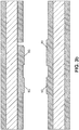
- the electrical power assembly 1 also comprises at least one open cavity 40 extending from an electrical contact 11 of the power die 10, through the electrically insulating core 20 and the surface layer of electrically conductive material 30 covering the insulating core 20.
- open cavity 40 it is understood that the cavity has a bottom 41 and an open end 42 opposite its bottom.
- the bottom 41 of the open cavity is formed by a portion of the electrical contact 11 of the power die, which is therefore exposed by the open cavity.
- the cavity has walls 43 extending from the bottom 41 to its open end 42, wherein each wall is formed 42 in part by a thickness 22 of the electrically insulating core 20 extending between the power die 10 and the main surface 21 of the electrically insulating core located on the same side of the power die 10 as the open cavity 40, and in part by the surface layer 30 of electrically conductive material covering said side of the insulating core 20.
- the shape of the open cavity 40 is indifferent, i.e. it can be a square, a rectangle, a U-shape, a L-shape, or it can be round, etc., but as will be explained in more detailed below, is preferably chosen to make the alignment of the power assembly on a substrate easier.
- the shape and profile of the cavity are advantageously configured to optimize electrical and thermal transports between the electrical power assembly and a substrate later assembled with the assembly.
- the portion of the electrical contact 11 of the power die 10 that is exposed by the open cavity has a surface comprised between 1 and 100% of the surface of the electrical contact. If there is only one open cavity exposing a portion of the electrical contact, the surface of the portion exposed by said cavity is preferably comprised between 10 and 100% of the surface of the electrical contact 11, and preferably between 50 and 100% of the surface of the electrical contact 11.
- the surface of the electrical contact exposed by each cavity is at least 1% of the surface of the electrical contact, and the cumulative surface of the electrical contact exposed by the cavities is comprised between 10 and 100% of the surface of the electrical contact, and preferably between 50 and 100% of the surface of the electrical contact.
- the open cavity 40 is shaped such that the power die 10 extends further than at least two opposite walls 43 of the cavity 40, and, in an embodiment, such that a peripheral edge of the power die is not exposed by the cavity.
- the electrically insulating core 20 comprises a rim 23 covering at least two opposite edges 12 of the power die, and preferably covering a peripheral edge of the power die, thereby maintaining the power die in its position in the electrically insulating core 10.
- the open cavity 40 is further at least partially plated with electrically conductive material (preferably copper) in order to connect the power die electrical contact 11 which is exposed by the open cavity to the surface layer 30 of electrically conductive material of the assembly 1.
- electrically conductive material preferably copper
- the power assembly 1 exhibits a contact pad for its connection to a substrate, which comprises at least the bottom of the cavity, the portion of the surface layer of electrically conductive material 30 to which it is connected and the plated part of the side walls 43 of the cavity.
- the open cavity 40 may be fully plated, i.e. the bottom of the cavity formed by the exposed area of the power die electrical contact, and the side walls of the cavity, may be fully plated, in order to increase a connection surface of the open cavity.
- the size of the gate pad may be too small to form an open cavity exposing the gate pad.
- the latter may be connected to the surface layer 30 of electrically conductive material by at least one via, obtained for instance by laser drilling. In that case the plating of the assembly 1 is also performed in order to plate the via and achieve the connection of the gate pad to the surface layer 30.
- the layer of electrically conductive material resulting from the plating of the bottom and side walls of the cavity is shown in the figures with reference 44.
- the metal of the electrical power assembly 1, i.e. the metal of the surface layer 30 and the metal used for the plating step is preferably copper, but it can be other material like silver.
- the assembly pads can also be finished by other metals in order to create a protection against oxidation, humidity, migration or other. These metals can be nickel, silver, tin or gold which can be deposited by any method like chemical, vaporization or other.
- the surface layer 30 of electrically conductive material located on the side of the power assembly in which the open cavity is located can comprise a superficial thickness 31 resulting from the plating of the whole side of the cell 1 in which the open cavity 40 is arranged.
- the assembly 1 has a contact pad comprising the plated surface layer 30, and the plated bottom 41 and walls 43 of the cavity 40.
- the thickness of the plating layer is preferably comprised between 2 and 100 ⁇ m, for instance about 10 ⁇ m.
- Open cavities 40 may be formed in the electrical power assembly 1 on opposite sides of the assembly in order to expose respective portions of opposite electrical contacts 11 of the power die 10 embedded in the insulating core 20. Alternatively, one electrical contact may be exposed thanks to an open cavity 40, and an opposite electrical contact 11 of the power die may be connected to an opposite surface layer 30 thanks to through vias 50 arranged in the electrically insulating core 20, as in the example shown in figure 1b .
- the assembly comprises at least one additional power die 10 or one or more passive components
- several open cavities 40 can be arranged on a same side of the cell to expose respective portions of the electrical contacts of the components embedded in the insulating core.
- the surface layer 30 of electrically conductive material which is connected to the electrical contacts of the components is preferably patterned to isolate electrical contacts of different components where applicable.
- the plating layer provides said connection.
- the electrical power assembly 1 may also comprise at least one open cavity extending from the side of the power die devoid of electrical contacts, through the insulating core and corresponding surface layer. Said open cavity can then be used for cooling of the power die as explained below.
- the electrical power assembly 1 comprises, on a top surface, a first open cavity 40 exposing the anode of the diode 10, a second open cavity 40 exposing the emitter of the IGBT 10', and a via exposing the gate of the IGBT 10'.
- the top surface of the assembly is fully plated, such that the bottom 41 and side walls 43 of each cavity 40 are plated, and the assembly 1 comprises a surface layer 30 of electrically conductive material resulting from the platting. Further, this surface layer is patterned to isolate on the one hand the anode of the diode and emitter of the IGBT (which are connected together) and on the other hand the gate of the IGBT.
- the bottom side of the assembly also comprises an open cavity 40 exposing the cathode of the diode 10, and an open cavity exposing the collector of the IGBT 10'.
- the bottom side is plated such that bottom 41 and side walls 43 of each cavity are plated, and the assembly comprises a surface 30 layer of electrically conductive material resulting from the platting. This layer needs not be patterned because it connects together the cathode and the collector.
- the electrical power assembly 1 comprises a single power die, for instance a diode, having two opposite electrical contacts 11, and the assembly comprises two opposite open cavities 40 exposing respective portions of the opposite electrical contacts 11.
- the electrical power assembly 1 comprises a single power die 10 having two opposite electrical contacts 11, and the assembly comprises one open cavity 40 exposing a portion of one electrical contact 11.
- a surface layer 30 of electrically conductive material is connected to the other electrical contact 11 of the power die by through vias 50.
- any of the described elementary assemblies can have at least one through hole via that connects at least part of the top conductive layer 30 to at least part of the bottom conductor layer 30 in order to transport at least one electric contact from one side of the assembly to the other side of the assembly (top to bottom or vice versa), or in order to duplicate on the conductor layers 30 located on both sides of the assembly at least one electric contact which originally exist on one side of the at least one power device.
- the size and number of the through hole vias of the at least one electric contact to be transported or duplicated is chosen according the current level to be conducted on these vias.
- the method comprises a first step 100 of forming a base structure 80 comprising at least an electrically insulating core 20, and layers 60 of electrically conductive material covering opposite main surfaces of the electrically insulating core 20, the insulating core 20 embedding at least one power die 10.
- the material of the electrically insulating core is preferably chosen has having low thermal resistance to provide better heat dissipation.
- the electrically insulating core 20 may be made of of epoxy resin such as FR-4 glass epoxy, of polyimide, or in ceramic such as HTCC (High-Temperature Co-fired Ceramic) or LTCC (Low Temperature Co-fired Ceramic).
- the power die 10 may be a diode or a transistor such as a MOSFET, JFET or IGBT, and can have the various configurations of electrical contacts 11 already detailed above.
- the electrical power assembly may comprise at least one additional power die, or a sensor such as a temperature sensor, field sensor, current sensor, or other, or at least one passive component such as a resistor, a capacitor, or other, connected to the first power die 10.
- a sensor such as a temperature sensor, field sensor, current sensor, or other
- at least one passive component such as a resistor, a capacitor, or other, connected to the first power die 10.
- the power dies can be of different types and references, have different orientations and different thicknesses.
- the base structure 80 comprises an IGBT 10' and a diode 10, embedded in respective cavities of the electrically insulating core 20.
- the diode has two electrical contacts 11, namely an anode and a cathode, and the IGBT has three electrical contacts 11', an emitter, a gate and a collector.
- the diode is inserted in the cavity of the insulating core 20 such that the anode is oriented towards the same main side of the insulating core 20 than the gate and emitter of the IGBT, i.e. towards the top side in the figures.
- the base structure 80 may be a PCB where the layer of electrically conductive material is made of copper and the electrically insulating core 20 is made of FR4, in which each power die is embedded.
- the base structure 80 can be obtained during step 100 by implementing a first sub-step 101 of forming at least one through-cavity 250 in a base layer 25 of electrically insulating material, the through-cavity 250 having the shape and dimensions of a power die to be embedded in the assembly.
- the through-cavity may be obtained for instance by mechanical drilling, milling, stamping or even laser cutting.
- the step 100 then comprises a sub-step 102 of inserting the power die 10 in the through-cavity 250, or as the case may be each power die 10, 10' in a respective cavity.
- Each power die inserted in a respective cavity is oriented such that each electrical contact 11 of the die extends parallel to the plane of the base layer 25 of electrically insulating material.
- the electrical contacts 11 also extend horizontally, each contact facing upwardly or downwardly.
- the electrical contacts of the die are exposed and are not facing a side wall of the through-cavity 250.
- the step 100 then comprises a sub-step 103 of inserting the base layer 25 comprising each power die 10 between two additional layers 26 of electrically insulating material of the same material than the first one, to obtain a stack 27 of electrically insulating material that will then become the electrically insulating core 20.
- a sub-step 103 two layers 60 of electrically conductive material such as copper are also provided, and the stack 27 of electrically insulating material is inserted between the two layers 60 of electrically conductive material.
- the stack 27 of electrically insulating material and the conductive layers 60 are laminated in order to form the base structure 80, in which the layers of the stack 27 are fused together to form the electrically insulating core 20.
- the electrical contacts of the power die are thus covered successively with a layer a layer 26 of electrically insulating material, and a layer 60 of electrically conductive material.
- the method then comprises a step 110 of forming at least one open cavity 40 in the base structure 80, the open cavity 40 exposing a portion of an electrical contact 11 of the power die 10 embedded in the insulating core 20.
- This step thus comprises the removal, from the base structure 80, of a stack comprising a portion of the electrically insulating core 20 adjacent the electrical contact 11 of the power die, and a corresponding portion of the layer 60 of electrically conductive material covering said portion of the core 20.
- the portion of the electrical contact 11 of the power die 10 exposed by the open cavity 40 after removal of this stack has a surface comprised between 10 and 100% of the surface of the electrical contact, and even more preferably between 50 and 100% of the surface of the electrical contact.
- exposed portion is preferably as large as possible in order to maximize the electrical and thermal contact surface of the assembly 1.
- a plurality of open cavities 40 can be made in the base structure to expose respective portions of a same electrical contact 11. This can be easier to implement than forming a single open cavity 40 exposing a large surface of the electrical contact.
- the surface of the electrical contact exposed by each cavity is comprised between 1 and 100% of the surface of the electrical contact, and the cumulative surface of the electrical contact exposed by the cavities is preferably comprised between 10 and 100% of the surface of the electrical contact, and even more preferably between 50 and 100% of said surface.
- the power die 10 has to remain maintained in position by the electrically insulating core 20 after formation of the open cavity 40. Therefore the open cavity 40 is dimensioned so as not to expose more than the electrical contact 11 of the power, and in particular the bottom 41 of the open cavity 40 cannot extend over the whole surface of the side of the power die on which the electrical contact is arranged.
- the open cavity 40 is shaped such that the power die 10 extends further than at least two opposite walls 43 of the cavity 40, and, in an embodiment, such that a peripheral edge of the power die is not exposed by the cavity.
- the electrically insulating core thus comprises, as shown in the example of figure 2 d , after formation of the cavity, at least two opposite edges 23 and optionally a peripheral edge adjacent the power die 10 and forming the base of the side walls 43 of the open cavity 40.
- the method then preferably comprises a step 120 of plating at least partially the open cavity 40 with electrically conductive material, which can be a metal and is preferably copper, in order to connect the exposed electrical contact 11 of the power die 10 to the layer 60 of electrically conductive material of the base structure.
- electrically conductive material which can be a metal and is preferably copper
- the plating may be performed by electro less or/and electro plating.
- At least part of the side walls 43 of the open cavity 40 extending from the bottom 41 of the cavity formed by the electrical contact 11 to the layer 60 of electrically conductive material, may be plated.
- the surface layer of the obtained electrical power assembly is formed by the layer 60 of electrically conductive material of the base structure.
- the open cavity 40 as well as the layer 60 of electrically conductive material of the base structure may be fully plated by deposition of an electrically conductive material such as copper.
- an electrically conductive material such as copper.
- the power die 10 comprises a gate pad, and a through via is formed in the electrically insulating core to access the gate pad. In that case the plating also allows electrically connecting the gate pad to the layer 60 of electrically conductive material thanks to the via.
- the surface layer 30 of the obtained electrical power assembly 1 is formed by the layer 60 of conductive material of the base structure on top of which is an additional thickness 31 of electrically conductive material which results from the plating.
- connection surface for enabling connection to the electrical contact of the power die is enlarged because it comprises:
- the method can then comprise an optional step 130 of patterning the surface layer 30 of electrically conductive material by etching, in order to isolate the electrical contacts that should not be connected together.
- the etching also may include etching the outer edges of layer 30 in order to increase the isolation distance between the opposite layers 30 of conductive material.
- This method can also comprise an optional step 140 of finishing the surface layer 30 by a different metal. This helps protecting the metal of layer 30 from different phenomena like oxidation or migration.
- the finish metal can be silver, gold, tin, titanium, nickel, chrome or other.
- the finish layer can be made of different metals or different layer of metals.
- the electrical power assembly comprises a diode and an IGBT
- the assembly comprises open cavities exposing respectively the anode, emitter and gate of the diode and IGBT
- the anode and emitter of the IGBT are connected together but the gate has to be isolated from the other electrical contacts. Therefore the patterning step is performed to remove a portion of the external layer of electrically conductive material connecting together the gate and other electrodes.
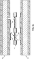
- a electrical power assembly 1 may be integrated into a power module 9 in order to be connected to other components.
- the power module 9 may comprise at least one substrate 90 comprising at least a layer 91 of electrically conductive material, and a layer 92 of thermally conductive material, which is also electrically insulating.
- the substrate may for instance be a Direct Bonded Copper (DBC) substrate, in which a patterned layer of copper is arranged on a ceramic plate (for instance made of alumina), forming the thermally conductive and electrically insulating layer.
- DBC Direct Bonded Copper
- the substrate may be an Insulated Metal Substrate (IMS) or an Active Metal Brazed (AMS) Substrate.
- the layer 91 of electrically conductive material may be patterned to provide proper electrical connection between various elementary components, and for instance between various power assemblies 1.
- the substrate comprises at least one post 93 of electrically conductive material protruding from the layer 91 of electrically conductive material, the post having a shape and dimensions corresponding to the shape and dimensions of a cavity of the elementary power assembly in order to allow insertion of the post inside the cavity of the elementary power assembly, such that insertion of the post inside the cavity allows electrical and thermal connection between the post and the electrical contact 11 of the power die exposed by the cavity.
- the open cavity 40 is at least partially plated, insertion of the post inside the open cavity may further allow electrical connection between the post and the plated walls (either bottom wall corresponding to the plated electrical contact of the power die or side walls) of the cavity.
- a power assembly 1 to be connected to the substrate 90 comprises several open cavities 40
- the substrate 90 comprises corresponding posts 93 of same sizes and dimensions that the respective cavities.
- the shape of a cavity is indifferent, however the shapes and orientations of various cavities of the power assembly are preferably chosen in order to allow unique orientation of the mating substrate relative to the assembly, and easy fitting to that substrate.
- the shape of the cavity is preferably chosen to permit a unique orientation of the substrate relative to the assembly, i.e. the shape may be a U-shape, a L-shape, a triangle, etc.
- an assembly comprises a plurality of cavities
- the shapes and orientations of the cavities are chosen to allow unique orientation of the mating substrate.
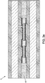
- a power module may comprise one such substrate 90 assembled to one side of an electrical power assembly where an open cavity 40 is arranged. If the power die has opposite electrical contacts 11, the opposite contact of the power die which is not exposed by the cavity 40 may be connected to an electrical pad of the assembly arranged on a side of the assembly opposite the cavity, for example by through vias, and the electrical pad may be connected to the substrate by wire bonding, as shown schematically on the example of figure 4 .
- the wire bonds 55 are preferably also made of copper, since it provides better thermal and electrical conductivities.
- the power module 9 comprises two substrates 90 between which is inserted the electrical power assembly 1, to provide double-sided cooling.
- the electrical power assembly preferably has at least two opposite open cavities 40 exposing respective portions of opposite electrical contacts 11 of the power die 10, and each substrate 90 comprises at least one post 93 shaped to be inserted in a respective cavity of the power die.
- the power module may also comprise two substrates 90 having posts 93 adapted to be inserted in corresponding open cavities, the post inserted in the open cavity on the side of the power die devoid of electrical contact allowing for dissipation of heat generated by the power die.
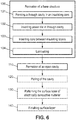
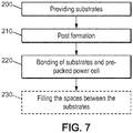
- a manufacturing method of such a power module comprises a step 200 of providing two substrates 90 comprising each a layer 91 of electrically conductive material and a layer 92 of thermally conductive and electrically insulating material ( fig. 3a ).
- the method then comprises a step 210 of forming at least one post 93 on at least one of the substrates 90 ( fig. 3b ).
- Each post 93 may be formed on a respective layer 91 of electrically conductive material either by additive manufacturing, for example by Chemical Vapor Deposition 3D or screen printing or any suitable method, or by subtractive manufacturing, for instance by chemically or mechanically etching a thicker layer of electrically conductive material to obtain the desired posts.
- the method then comprises a step 220 of positioning an elementary power assembly between the substrates ( fig. 3c ), such that each post of a substrate is inserted in a corresponding cavity of the power assembly, and bonding together ( fig. 3d ) the substrates and power assembly.
- the bonding may be performed by soldering, sintering, gluing, or the assembly may be pressed to the substrates directly or using a conductive material preform such as molybdenum preform.
- Any suitable bonding layer 94 may be deposited in order to perform the bonding, such as conductive glue for gluing, soldering material, or sintering paste such as silver or copper sintering paste.
- the bonding layer may in that case be deposited on at least a portion of each layer of electrically conductive material of the substrates.
- the bonding layer 94 may in particular be deposited at least on each post 93 of each layer of electrically conductive material.
- the bonding layer 94 is deposited on all a surface of the electrically conductive material that will then be adhered to an outer surface of the elementary power assembly.
- the adhesive material may be sintering paste, such as silver sintering paste.
- the method also comprises a step 230 of filling the empty spaces between the substrates by an injectable electrically isolating material 95.
- Said material can be silicone gel, epoxy, or plastic, etc...
- the filling material 95 may also be adhesive in order to hold together both substrates 90.
- the power module 9 thus obtained has improved thermal performances compared to traditional PCB embedding as the metal posts not only provide electrical connection to the power die, but they also allow thermal dissipation of the heat generated by the power die.
- the use of cavities and corresponding metal posts implies that no thick metal deposition is needed on the elementary power assembly 1, which reduces the time and cost of the manufacturing operation.
- the cavities and metal posts improve the alignment of the power dies relative to the substrates that they have to be connected to, because the configuration of the cavities and posts are made in order to easily imbricate the assembly with the substrate.
Description
- The invention relates to an electrical power assembly comprising a power die embedded in an insulating core, the power assembly providing a better connection and alignment of the power die to a substrate. The invention also relates to a manufacturing method of the power assembly, and to a power module comprising one or two substrates assembled to said electrical power assembly.
-
WO2015077808 discloses a circuit board structure for mounting a power component. - Power dies, such as diodes or various types of transistors (MOSFET, JFT, IGBT...) are elementary components of power modules which are used for the control and conversion of electric power, for instance in applications such as the automotive or aeronautic industries.
- Currently the most common way to connect a power die to other components, for instance in a power module, is by using an insulated plate such as Direct Bonded Commer (DBC) Substrate, which comprises a ceramic tile covered on at least one side with a sheet of copper. Power dies are soldered or sintered on the DBC Susbtrate on one side, and connected on the other side of the die by wire bonds or ribbons of aluminum that are ultrasonic welded on the die metallization.
- The constant increase in switching frequency and power density of power dies leads to a constant need for thermal enhancement, volume reduction and reliability increase of power modules.
- In this perspective, the traditional connection by wire bonding of a power die on a substrate has a number limitations and drawbacks, among which the serial and long manufacturing process due to the small size of some dies electrical contacts (in particular gate pads), and the high parasitic level and low reliability of the wire bonds.
- It has recently been proposed power modules which comprise two cooling substrates such as DBCs, between which are sandwiched power dies.
- For instance, document
US6442033 discloses a power module comprising two insulated metal substrates, between which are interposed a plurality of power devices. As another example, documentUS8432030 discloses a power electronic package comprising two substrates between which are mounted multiple power dies. The substrates comprise raised regions or posts providing electrical and mechanical connections between the substrates, and/or between the substrates and the power dies. - The modules proposed in these documents eliminate the need for wire bonds, thereby exhibiting higher reliability, and provide double sided cooling.
- However, these modules are quite complex to manufacture, because of the very small size of the power dies electrodes, and in particular of the gate pads. It is indeed quite complicated to align the power dies electrical contacts with two substrates, especially when the substrates comprise thick copper layers, which is the case for many power electronic applications.
- Another emerging technology is to manufacture pre-packed power cells, comprising at least one power die embedded in a PCB laminate. It is for example known from document
US 9425131 a - This type of package allows easier connection of the power die's electrical contact on a substrate. In addition, the embedding of the die inside a substrate reduces the mechanical stresses on the die during assembly stage and increases the reliability and lifetime of the die.
- However, in such pre-package power cell, the power devices are connected by vias on the device pads through insulated layers. Even with high number of copper vias which is usually limited by manufacturing capabilities, the connection layer made of copper vias and insulation material presents a high thermal resistance compared to the direct contact by soldering and silver sintering in traditional power modules. In addition, in order to obtain higher thermal and electrical performances of the power cell, it is preferable to have vias filled with copper and a thicker copper layer on the pre-packaged cell. This required longer copper plating time which increases significantly the manufacturing time and cost.
- The invention aims at solving at least part of the problems listed above. In particular, the invention aims at providing a package for a power die allowing easy connection to the power die for power application.
- Another aim of the invention is to propose an electrical power assembly providing easy alignment relative to a substrate.
- Another aim of the invention is to propose a power module which is easier and less expensive to manufacture.
- Accordingly, a power module according to
claim 1 is disclosed. Additional features are specified in dependent claims 2-7. - In an embodiment, the power module comprises two substrates each comprising a layer of thermally conductive and electrically insulating material and a layer of electrically conductive material having a post protruding thereof, and wherein the electrical power assembly comprises open cavities on opposite sides thereof, the power assembly being mounted between the two substrates with each post of a substrate being inserted in a respective cavity of the power cell, and the power module further comprises electrically isolating material filling the spaces remaining between the substrates.
- According to another object of the invention, a method according to claim 8 Z for manufacturing a power module is disclosed. Additional features are specified in dependent claims 9-13.
- An electrical power assembly according to the invention provides a number of advantages. Indeed, the electrical power assembly according to the invention comprises at least an open cavity which simultaneously plays two roles. The first role of the open cavity is to expose an electrical contact of the power die, thereby allowing its direct connection to a substrate. This direct connection allows transmission of high power with a low manufacturing cost.
- It is thus not necessary to provide a thick copper layer for connecting the power die to the substrate, and the manufacturing process of the power assembly is therefore quicker and cheaper.
- In some embodiments, the bottom and walls of the cavity may also be plated to connect the power die electrical contact with the surface layer of electrically conductive material of the power assembly. This can allow easy connection, for instance between several components embedded in the assembly.
- The other role of the open cavity is to facilitate the subsequent alignment of the power assembly with a substrate, because the substrate can comprise a corresponding post adapted to be inserted in the open cavity to provide electrical connection between the substrate and the power die.
- A power module comprising at least one substrate and such an electrical power assembly is thus easier to align and assemble.
- For enhanced thermal dissipation, a double sided cooling power module can be obtained by positioning a power assembly having cavities formed on opposite sides of the power die between two substrates, each substrate having posts shaped to be inserted into the corresponding cavities.
- Other features and advantages of the invention will be apparent from the following detailed description given by way of non-limiting example, with reference to the accompanying drawings, in which:
-
Figures 1a and 1b represent two examples of electrical power assemblies comprised in the power module according toclaim 1, -
Figures 2a to 2f schematically represent an example of a method for manufacturing an electrical power assembly comprised in the power module according toclaim 1, -
Figures 3a to 3e schematically represent an example of a method for manufacturing a power module according to an embodiment of the invention. -
Figure 4 represents an example of a power module according to an embodiment of the invention. -
Figure 5 is the electrical diagram of an elementary power assembly comprising an IGBT and a diode. -
Figure 6 schematically illustrates the main steps of a method of manufacturing an electrical power assembly comprised in the power module according toclaim 1, -
Figure 7 schematically illustrates the main steps of a method of manufacturing a power module according to an embodiment of the invention. - With reference to
figures 1a, 1b and2f , anelectrical power assembly 1 comprised in the power module according toclaim 1 will now be described. Theelectrical power assembly 1 is used as an elementary component for integration in a power module and/or a power converter as will be explained in more details below. - The
electrical power assembly 1 comprises apower die 10. The power die may be a diode or a transistor such as a MOSFET, JFET or IGBT. In embodiments, the power die 10 is made from silicon semiconductor or a wide bandgap semiconductor, i.e. a semiconductor having a bandgap in the range of 2-4 eV. For instance, the power die may be made in Silicon Carbide SiC or in Gallium Nitride GaN. - The power die has at least two
electrical contacts 11. The electrical contacts are metallic pads made of any suitable metal such as aluminum, gold, copper, silver, etc. The power die may be a lateral component in which theelectrical contacts 11 are arranged on a same side of the die. Else, the power die may be a vertical component in which theelectrical contacts 11 are arranged on opposite sides of the die. - For instance, the power die 10 can be a diode having two opposite
electrical contacts 11. According to another example, the power die 10 can be a transistor having three electrical contacts comprising a gate, a source, and a drain, or a gate, an emitter and a collector, according to the type of transistor. - The electrical power assembly may comprise at least one additional power die or a sensor such as a temperature sensor, a field sensor, a current sensor, or other, or at least one passive component such as a resistor, a capacitor, or other, connected to the first power die 10. In case of at least two power dies 10 included in the electrical power assembly, the power dies can be of different types and references, have different orientations and different thicknesses.
- A non-limiting example is shown schematically in
figure 2f , in which theelectrical power assembly 1 comprises an IGBT 10' having on a top side a gate and an emitter and on a bottom side a collector, and adiode 10 having a top pad as an anode, connected to the emitter, and a bottom pad as a cathode, connected to the collector. Due to this arrangement theelectrical power assembly 1 forms a switch to be used in a power module, corresponding to the electrical diagram shown infigure 5 . - The
electrical power assembly 1 comprises an electrically insulatingcore 20, in which the, or each power die 10, is embedded. The power die 10 is embedded in the insulatingcore 20 such that each electrical contact of the power die extends along a plane which is substantially parallel to a main plane along which extends the core. - Moreover, if the power die 10 comprises opposite
electrical contacts 11 extending parallel to one another, the direction extending between the contacts and being orthogonal to each contact is also orthogonal to the main plane along which extends the electrically insulating core. This is the case in the figures in which the power dies are shown having a vertical arrangement, while the insulating core extends along a horizontal plane. - The material of the electrically insulating core is preferably chosen as having low thermal resistance to provide better heat dissipation.
- As non-limiting examples, the electrically insulating
core 20 may be made of of epoxy resin such as FR-4 glass epoxy, of polyimide, or in ceramic such as HTCC (High-Temperature Co-fired Ceramic) or LTCC (Low Temperature Co-fired Ceramic). - The electrically insulating
core 20 comprising the power die 10 extends sensibly along a plane and defines two oppositemain surfaces 21 which extend substantially along said plane. - The
electrical power assembly 1 further comprises twosurface layers 30 of electrically conductive material on opposite main surfaces of the insulatingcore 20. The material of these layers is a metal, preferably copper. - Each
electrical contact 11 of the power die 10 is connected to one of the surface layers 30. If twoelectrical contacts 11 are located on the same side of the die 10, they can be connected to the same surface layer and, if required electrically, the latter is preferably patterned to disconnect the two electrical contacts. - As shown in
figures 1a, 1b and2f , theelectrical power assembly 1 also comprises at least oneopen cavity 40 extending from anelectrical contact 11 of the power die 10, through the electrically insulatingcore 20 and the surface layer of electricallyconductive material 30 covering the insulatingcore 20. - By
open cavity 40 it is understood that the cavity has a bottom 41 and anopen end 42 opposite its bottom. The bottom 41 of the open cavity is formed by a portion of theelectrical contact 11 of the power die, which is therefore exposed by the open cavity. - The cavity has
walls 43 extending from the bottom 41 to itsopen end 42, wherein each wall is formed 42 in part by athickness 22 of the electrically insulatingcore 20 extending between the power die 10 and themain surface 21 of the electrically insulating core located on the same side of the power die 10 as theopen cavity 40, and in part by thesurface layer 30 of electrically conductive material covering said side of the insulatingcore 20. - The shape of the
open cavity 40, as seen looking towards the bottom of the cavity, is indifferent, i.e. it can be a square, a rectangle, a U-shape, a L-shape, or it can be round, etc., but as will be explained in more detailed below, is preferably chosen to make the alignment of the power assembly on a substrate easier. - Additionally, the shape and profile of the cavity are advantageously configured to optimize electrical and thermal transports between the electrical power assembly and a substrate later assembled with the assembly.
- Preferably, the portion of the
electrical contact 11 of the power die 10 that is exposed by the open cavity has a surface comprised between 1 and 100% of the surface of the electrical contact. If there is only one open cavity exposing a portion of the electrical contact, the surface of the portion exposed by said cavity is preferably comprised between 10 and 100% of the surface of theelectrical contact 11, and preferably between 50 and 100% of the surface of theelectrical contact 11. - Several adjacent cavities may also be formed in the electrical power assembly to expose respective portions of a same electrical contact of the power die. In that case, the surface of the electrical contact exposed by each cavity is at least 1% of the surface of the electrical contact, and the cumulative surface of the electrical contact exposed by the cavities is comprised between 10 and 100% of the surface of the electrical contact, and preferably between 50 and 100% of the surface of the electrical contact.
- In addition, the
open cavity 40 is shaped such that the power die 10 extends further than at least twoopposite walls 43 of thecavity 40, and, in an embodiment, such that a peripheral edge of the power die is not exposed by the cavity. - Due to this configuration, the electrically insulating
core 20 comprises arim 23 covering at least twoopposite edges 12 of the power die, and preferably covering a peripheral edge of the power die, thereby maintaining the power die in its position in the electrically insulatingcore 10. - In preferred embodiments, the
open cavity 40 is further at least partially plated with electrically conductive material (preferably copper) in order to connect the power dieelectrical contact 11 which is exposed by the open cavity to thesurface layer 30 of electrically conductive material of theassembly 1. - Thus, the
power assembly 1 exhibits a contact pad for its connection to a substrate, which comprises at least the bottom of the cavity, the portion of the surface layer of electricallyconductive material 30 to which it is connected and the plated part of theside walls 43 of the cavity. - Preferably, the
open cavity 40 may be fully plated, i.e. the bottom of the cavity formed by the exposed area of the power die electrical contact, and the side walls of the cavity, may be fully plated, in order to increase a connection surface of the open cavity. - Moreover, in the case where the power die 10 comprises a gate pad or any other small pads such as on-chip sensor or temperature sensors, the size of the gate pad may be too small to form an open cavity exposing the gate pad. Thus in order to allow connection of the gate pad, the latter may be connected to the
surface layer 30 of electrically conductive material by at least one via, obtained for instance by laser drilling. In that case the plating of theassembly 1 is also performed in order to plate the via and achieve the connection of the gate pad to thesurface layer 30. - The layer of electrically conductive material resulting from the plating of the bottom and side walls of the cavity is shown in the figures with
reference 44. - The metal of the
electrical power assembly 1, i.e. the metal of thesurface layer 30 and the metal used for the plating step is preferably copper, but it can be other material like silver. The assembly pads can also be finished by other metals in order to create a protection against oxidation, humidity, migration or other. These metals can be nickel, silver, tin or gold which can be deposited by any method like chemical, vaporization or other. - As will be explained in more details below, and as is the case in the examples of
figure 1a, 1b and2d , thesurface layer 30 of electrically conductive material located on the side of the power assembly in which the open cavity is located can comprise asuperficial thickness 31 resulting from the plating of the whole side of thecell 1 in which theopen cavity 40 is arranged. In that case, theassembly 1 has a contact pad comprising the platedsurface layer 30, and the plated bottom 41 andwalls 43 of thecavity 40. - The thickness of the plating layer, either in the cavity or on a main surface of the assembly, is preferably comprised between 2 and 100 µm, for instance about 10 µm.
-
Open cavities 40 may be formed in theelectrical power assembly 1 on opposite sides of the assembly in order to expose respective portions of oppositeelectrical contacts 11 of the power die 10 embedded in the insulatingcore 20. Alternatively, one electrical contact may be exposed thanks to anopen cavity 40, and an oppositeelectrical contact 11 of the power die may be connected to anopposite surface layer 30 thanks to throughvias 50 arranged in the electrically insulatingcore 20, as in the example shown infigure 1b . - In addition, if the assembly comprises at least one additional power die 10 or one or more passive components, several
open cavities 40 can be arranged on a same side of the cell to expose respective portions of the electrical contacts of the components embedded in the insulating core. - In that case, the
surface layer 30 of electrically conductive material which is connected to the electrical contacts of the components is preferably patterned to isolate electrical contacts of different components where applicable. In cases where a connection is desired between the electrical contacts of the components, the plating layer provides said connection. - If the power die 10 embedded in the power assembly is a lateral component having all electrical contacts on the same side of the power die, the
electrical power assembly 1 may also comprise at least one open cavity extending from the side of the power die devoid of electrical contacts, through the insulating core and corresponding surface layer. Said open cavity can then be used for cooling of the power die as explained below. - This is the case in the example shown in
figure 2f of an electrical power assembly corresponding to the electrical diagram offigure 5 . In this example theelectrical power assembly 1 comprises, on a top surface, a firstopen cavity 40 exposing the anode of thediode 10, a secondopen cavity 40 exposing the emitter of the IGBT 10', and a via exposing the gate of the IGBT 10'. - The top surface of the assembly is fully plated, such that the bottom 41 and
side walls 43 of eachcavity 40 are plated, and theassembly 1 comprises asurface layer 30 of electrically conductive material resulting from the platting. Further, this surface layer is patterned to isolate on the one hand the anode of the diode and emitter of the IGBT (which are connected together) and on the other hand the gate of the IGBT. - The bottom side of the assembly also comprises an
open cavity 40 exposing the cathode of thediode 10, and an open cavity exposing the collector of the IGBT 10'. The bottom side is plated such that bottom 41 andside walls 43 of each cavity are plated, and the assembly comprises asurface 30 layer of electrically conductive material resulting from the platting. This layer needs not be patterned because it connects together the cathode and the collector. - According to another example shown schematically in
figure 1a , theelectrical power assembly 1 comprises a single power die, for instance a diode, having two oppositeelectrical contacts 11, and the assembly comprises two oppositeopen cavities 40 exposing respective portions of the oppositeelectrical contacts 11. - According to still another example shown schematically in
figure 1b , theelectrical power assembly 1 comprises a single power die 10 having two oppositeelectrical contacts 11, and the assembly comprises oneopen cavity 40 exposing a portion of oneelectrical contact 11. On the other side of the assembly, asurface layer 30 of electrically conductive material is connected to the otherelectrical contact 11 of the power die by throughvias 50. - Any of the described elementary assemblies can have at least one through hole via that connects at least part of the top
conductive layer 30 to at least part of thebottom conductor layer 30 in order to transport at least one electric contact from one side of the assembly to the other side of the assembly (top to bottom or vice versa), or in order to duplicate on the conductor layers 30 located on both sides of the assembly at least one electric contact which originally exist on one side of the at least one power device. The size and number of the through hole vias of the at least one electric contact to be transported or duplicated is chosen according the current level to be conducted on these vias. - With reference to
figures 2a to 2f and tofigure 6 , a manufacturing method of an electrical power assembly will now be described. - The method comprises a
first step 100 of forming abase structure 80 comprising at least an electrically insulatingcore 20, and layers 60 of electrically conductive material covering opposite main surfaces of the electrically insulatingcore 20, the insulatingcore 20 embedding at least one power die 10. - As already indicated above, the material of the electrically insulating core is preferably chosen has having low thermal resistance to provide better heat dissipation.
- As non-limiting examples, the electrically insulating
core 20 may be made of of epoxy resin such as FR-4 glass epoxy, of polyimide, or in ceramic such as HTCC (High-Temperature Co-fired Ceramic) or LTCC (Low Temperature Co-fired Ceramic). - The power die 10 may be a diode or a transistor such as a MOSFET, JFET or IGBT, and can have the various configurations of
electrical contacts 11 already detailed above. - The electrical power assembly may comprise at least one additional power die, or a sensor such as a temperature sensor, field sensor, current sensor, or other, or at least one passive component such as a resistor, a capacitor, or other, connected to the first power die 10. In case of at least two power dies 10 included in the electrical power assembly, the power dies can be of different types and references, have different orientations and different thicknesses.
- In the non-limiting examples of
figures 2a to 2f , thebase structure 80 comprises an IGBT 10' and adiode 10, embedded in respective cavities of the electrically insulatingcore 20. The diode has twoelectrical contacts 11, namely an anode and a cathode, and the IGBT has three electrical contacts 11', an emitter, a gate and a collector. - The diode is inserted in the cavity of the insulating
core 20 such that the anode is oriented towards the same main side of the insulatingcore 20 than the gate and emitter of the IGBT, i.e. towards the top side in the figures. - The
base structure 80 may be a PCB where the layer of electrically conductive material is made of copper and the electrically insulatingcore 20 is made of FR4, in which each power die is embedded. - In that case, the
base structure 80 can be obtained duringstep 100 by implementing afirst sub-step 101 of forming at least one through-cavity 250 in abase layer 25 of electrically insulating material, the through-cavity 250 having the shape and dimensions of a power die to be embedded in the assembly. - The through-cavity may be obtained for instance by mechanical drilling, milling, stamping or even laser cutting.
- The
step 100 then comprises a sub-step 102 of inserting the power die 10 in the through-cavity 250, or as the case may be each power die 10, 10' in a respective cavity. Each power die inserted in a respective cavity is oriented such that eachelectrical contact 11 of the die extends parallel to the plane of thebase layer 25 of electrically insulating material. In the figures, in which thelayer 25 of electrically insulating material extends horizontally, theelectrical contacts 11 also extend horizontally, each contact facing upwardly or downwardly. In other words, after thisstep 120 during which the power die is inserted in a through-cavity of thelayer 21, the electrical contacts of the die are exposed and are not facing a side wall of the through-cavity 250. - An exemplary implementation of this step is shown for instance in
figure 2a . - With reference to
figure 2b , thestep 100 then comprises a sub-step 103 of inserting thebase layer 25 comprising each power die 10 between twoadditional layers 26 of electrically insulating material of the same material than the first one, to obtain astack 27 of electrically insulating material that will then become the electrically insulatingcore 20. During this sub-step 103, twolayers 60 of electrically conductive material such as copper are also provided, and thestack 27 of electrically insulating material is inserted between the twolayers 60 of electrically conductive material. - With reference to
figure 2c , during a sub-step 104, thestack 27 of electrically insulating material and theconductive layers 60 are laminated in order to form thebase structure 80, in which the layers of thestack 27 are fused together to form the electrically insulatingcore 20. - Given the orientation of the power die 10 when inserted in the through-cavity of the insulating
base layer 25, the electrical contacts of the power die are thus covered successively with a layer alayer 26 of electrically insulating material, and alayer 60 of electrically conductive material. - With reference to
figure 2d , the method then comprises astep 110 of forming at least oneopen cavity 40 in thebase structure 80, theopen cavity 40 exposing a portion of anelectrical contact 11 of the power die 10 embedded in the insulatingcore 20. This step thus comprises the removal, from thebase structure 80, of a stack comprising a portion of the electrically insulatingcore 20 adjacent theelectrical contact 11 of the power die, and a corresponding portion of thelayer 60 of electrically conductive material covering said portion of thecore 20. - Preferably, and as already mentioned above, the portion of the
electrical contact 11 of the power die 10 exposed by theopen cavity 40 after removal of this stack has a surface comprised between 10 and 100% of the surface of the electrical contact, and even more preferably between 50 and 100% of the surface of the electrical contact. - Indeed, exposed portion is preferably as large as possible in order to maximize the electrical and thermal contact surface of the
assembly 1. - For power dies having electrical contacts of large dimensions (such as, for instance...), a plurality of
open cavities 40 can be made in the base structure to expose respective portions of a sameelectrical contact 11. This can be easier to implement than forming a singleopen cavity 40 exposing a large surface of the electrical contact. - In that case, the surface of the electrical contact exposed by each cavity is comprised between 1 and 100% of the surface of the electrical contact, and the cumulative surface of the electrical contact exposed by the cavities is preferably comprised between 10 and 100% of the surface of the electrical contact, and even more preferably between 50 and 100% of said surface.
- However, preferably the power die 10 has to remain maintained in position by the
electrically insulating core 20 after formation of theopen cavity 40. Therefore theopen cavity 40 is dimensioned so as not to expose more than theelectrical contact 11 of the power, and in particular the bottom 41 of theopen cavity 40 cannot extend over the whole surface of the side of the power die on which the electrical contact is arranged. - More specifically, the
open cavity 40 is shaped such that the power die 10 extends further than at least twoopposite walls 43 of thecavity 40, and, in an embodiment, such that a peripheral edge of the power die is not exposed by the cavity. - The electrically insulating core thus comprises, as shown in the example of
figure 2 d , after formation of the cavity, at least twoopposite edges 23 and optionally a peripheral edge adjacent the power die 10 and forming the base of theside walls 43 of theopen cavity 40. - With reference to
figure 2e , the method then preferably comprises astep 120 of plating at least partially theopen cavity 40 with electrically conductive material, which can be a metal and is preferably copper, in order to connect the exposedelectrical contact 11 of the power die 10 to thelayer 60 of electrically conductive material of the base structure. The plating may be performed by electro less or/and electro plating. - Therefore, at least part of the
side walls 43 of theopen cavity 40, extending from the bottom 41 of the cavity formed by theelectrical contact 11 to thelayer 60 of electrically conductive material, may be plated. - In an embodiment, only the side walls, and possibly the bottom of the
cavity 40 are plated. In that case, the surface layer of the obtained electrical power assembly is formed by thelayer 60 of electrically conductive material of the base structure. - According to a preferred embodiment, the
open cavity 40 as well as thelayer 60 of electrically conductive material of the base structure may be fully plated by deposition of an electrically conductive material such as copper. This embodiment is elected if the power die 10 comprises a gate pad, and a through via is formed in the electrically insulating core to access the gate pad. In that case the plating also allows electrically connecting the gate pad to thelayer 60 of electrically conductive material thanks to the via. - If the side of the base structure having the open cavity is fully plated, the
surface layer 30 of the obtainedelectrical power assembly 1 is formed by thelayer 60 of conductive material of the base structure on top of which is anadditional thickness 31 of electrically conductive material which results from the plating. - Thanks to the method, the connection surface for enabling connection to the electrical contact of the power die is enlarged because it comprises:
- The portion of the electrical contact of the power die exposed by the open cavity (which can be plated),
- The plated walls of the cavity, and
- The
surface layer 30 of the base structure which is connected to theelectrical contact 11. - This, combined with the direct contact with the power die electrical contact provided by the cavity, makes it not necessary to provide a thick plating layer to allow proper connection to the power die for power applications. For instance, a 5 µm-
thick plating layer - The method can then comprise an
optional step 130 of patterning thesurface layer 30 of electrically conductive material by etching, in order to isolate the electrical contacts that should not be connected together. The etching also may include etching the outer edges oflayer 30 in order to increase the isolation distance between theopposite layers 30 of conductive material. - This method can also comprise an
optional step 140 of finishing thesurface layer 30 by a different metal. This helps protecting the metal oflayer 30 from different phenomena like oxidation or migration. The finish metal can be silver, gold, tin, titanium, nickel, chrome or other. The finish layer can be made of different metals or different layer of metals. - In the example shown in
figure 2f , where the electrical power assembly comprises a diode and an IGBT, and the assembly comprises open cavities exposing respectively the anode, emitter and gate of the diode and IGBT, the anode and emitter of the IGBT are connected together but the gate has to be isolated from the other electrical contacts. Therefore the patterning step is performed to remove a portion of the external layer of electrically conductive material connecting together the gate and other electrodes. - Once a
electrical power assembly 1 is obtained, it may be integrated into apower module 9 in order to be connected to other components. - With reference to
figures 3e and4 , thepower module 9 may comprise at least onesubstrate 90 comprising at least alayer 91 of electrically conductive material, and alayer 92 of thermally conductive material, which is also electrically insulating. - The substrate may for instance be a Direct Bonded Copper (DBC) substrate, in which a patterned layer of copper is arranged on a ceramic plate (for instance made of alumina), forming the thermally conductive and electrically insulating layer. According to other examples, the substrate may be an Insulated Metal Substrate (IMS) or an Active Metal Brazed (AMS) Substrate.
- The
layer 91 of electrically conductive material may be patterned to provide proper electrical connection between various elementary components, and for instance betweenvarious power assemblies 1. - The substrate comprises at least one
post 93 of electrically conductive material protruding from thelayer 91 of electrically conductive material, the post having a shape and dimensions corresponding to the shape and dimensions of a cavity of the elementary power assembly in order to allow insertion of the post inside the cavity of the elementary power assembly, such that insertion of the post inside the cavity allows electrical and thermal connection between the post and theelectrical contact 11 of the power die exposed by the cavity. - Therefore, a direct electrical contact is obtained between the power die and the substrate.
- In addition, if the
open cavity 40 is at least partially plated, insertion of the post inside the open cavity may further allow electrical connection between the post and the plated walls (either bottom wall corresponding to the plated electrical contact of the power die or side walls) of the cavity. - If the main surface of the
power assembly 1 on which an open cavity is formed is fully plated, insertion of the post inside the open cavity further allows electrical connection between the surface layer of electrically conductive material of the power assembly and the layer of electrically conductive material of the substrate. - If a
power assembly 1 to be connected to thesubstrate 90 comprises severalopen cavities 40, thesubstrate 90 comprises correspondingposts 93 of same sizes and dimensions that the respective cavities. - As already indicated above, the shape of a cavity is indifferent, however the shapes and orientations of various cavities of the power assembly are preferably chosen in order to allow unique orientation of the mating substrate relative to the assembly, and easy fitting to that substrate.
- For instance, if an assembly comprises a single cavity, the shape of the cavity is preferably chosen to permit a unique orientation of the substrate relative to the assembly, i.e. the shape may be a U-shape, a L-shape, a triangle, etc.
- If an assembly comprises a plurality of cavities, the shapes and orientations of the cavities are chosen to allow unique orientation of the mating substrate.
- According to an embodiment, a power module may comprise one
such substrate 90 assembled to one side of an electrical power assembly where anopen cavity 40 is arranged. If the power die has oppositeelectrical contacts 11, the opposite contact of the power die which is not exposed by thecavity 40 may be connected to an electrical pad of the assembly arranged on a side of the assembly opposite the cavity, for example by through vias, and the electrical pad may be connected to the substrate by wire bonding, as shown schematically on the example offigure 4 . - If the
surface layer 30 of electrically conductive material of the assembly that is connected to theelectrical contact 11 of the power die by throughvias 50 is made of copper, thewire bonds 55 are preferably also made of copper, since it provides better thermal and electrical conductivities. - According to a preferred embodiment the
power module 9 comprises twosubstrates 90 between which is inserted theelectrical power assembly 1, to provide double-sided cooling. In that case the electrical power assembly preferably has at least two oppositeopen cavities 40 exposing respective portions of oppositeelectrical contacts 11 of the power die 10, and eachsubstrate 90 comprises at least onepost 93 shaped to be inserted in a respective cavity of the power die. - In an embodiment where the electrical power assembly comprises a lateral power die having all electrical contacts on the same side, and also comprises at least one cavity for connecting one of the electrical contacts and an additional open cavity extending from the side of the power die devoid of electrical contact, the power module may also comprise two
substrates 90 havingposts 93 adapted to be inserted in corresponding open cavities, the post inserted in the open cavity on the side of the power die devoid of electrical contact allowing for dissipation of heat generated by the power die. - With reference to
figures 3a to 3e and7 , a manufacturing method of such a power module comprises astep 200 of providing twosubstrates 90 comprising each alayer 91 of electrically conductive material and alayer 92 of thermally conductive and electrically insulating material (fig. 3a ). - The method then comprises a
step 210 of forming at least onepost 93 on at least one of the substrates 90 (fig. 3b ). Eachpost 93 may be formed on arespective layer 91 of electrically conductive material either by additive manufacturing, for example by Chemical Vapor Deposition 3D or screen printing or any suitable method, or by subtractive manufacturing, for instance by chemically or mechanically etching a thicker layer of electrically conductive material to obtain the desired posts. - The method then comprises a
step 220 of positioning an elementary power assembly between the substrates (fig. 3c ), such that each post of a substrate is inserted in a corresponding cavity of the power assembly, and bonding together (fig. 3d ) the substrates and power assembly. The bonding may be performed by soldering, sintering, gluing, or the assembly may be pressed to the substrates directly or using a conductive material preform such as molybdenum preform. - Any
suitable bonding layer 94 may be deposited in order to perform the bonding, such as conductive glue for gluing, soldering material, or sintering paste such as silver or copper sintering paste. The bonding layer may in that case be deposited on at least a portion of each layer of electrically conductive material of the substrates. Thebonding layer 94 may in particular be deposited at least on eachpost 93 of each layer of electrically conductive material. Preferably, thebonding layer 94 is deposited on all a surface of the electrically conductive material that will then be adhered to an outer surface of the elementary power assembly. - The adhesive material may be sintering paste, such as silver sintering paste.
- Preferably, as shown in
figure 3e , the method also comprises astep 230 of filling the empty spaces between the substrates by an injectableelectrically isolating material 95. Said material can be silicone gel, epoxy, or plastic, etc...In an embodiment, the fillingmaterial 95 may also be adhesive in order to hold together bothsubstrates 90. - The
power module 9 thus obtained has improved thermal performances compared to traditional PCB embedding as the metal posts not only provide electrical connection to the power die, but they also allow thermal dissipation of the heat generated by the power die. In addition, the use of cavities and corresponding metal posts implies that no thick metal deposition is needed on theelementary power assembly 1, which reduces the time and cost of the manufacturing operation. - Last, the cavities and metal posts improve the alignment of the power dies relative to the substrates that they have to be connected to, because the configuration of the cavities and posts are made in order to easily imbricate the assembly with the substrate.
Claims (13)
- A power module (9), comprising an electrical power assembly (1), the electrical power assembly (1) comprising :- a power die (10), having at least two electrical contacts (11),- an electrically insulating core (20), wherein the power die (10) is embedded in the electrically insulating core (20), and- two layers (60, 30) of electrically conductive material on opposite main surfaces of the electrically insulating core (20),- at least one open cavity (40) extending from an electrical contact (11) of the power die, through the electrically insulating core (20) and the layer (60, 30) of electrically conductive material located on the same side of the power die as the electrical contact, such that the open cavity (40) has a bottom (41) formed by an area of the electrical contact (11) of the power die,wherein the bottom (41), and side walls (43) of the open cavity (40) are at least partially plated with electrically conductive material to connect said area of the electrical contact (11) of the power die (10) to the layer (60, 30) of electrically conductive material, characterised in that
the power module (9) also comprises at least one substrate (90) comprising a layer of thermally conductive and electrically insulating material (92) and a layer (91) of electrically conductive material,
the substrate (90) further comprising at least one post (93) of electrically conductive material protruding from the layer of electrically conductive material (91), and the electrical power assembly (1) being mounted on the substrate (90) such that the post (93) is inserted in the open cavity (40) of the electrical power assembly (1),
said post (93) having a shape and dimensions adapted to the shape and dimensions of the open cavity (40) of the electrical power assembly (1), such that insertion of the post in said open cavity (40) provides electrical and thermal contact between the post (93) and the electrical contact (11) of the power die (10) from which the open cavity (40) extends. - A power module (9) according to claim 1, wherein, in the electrical power assembly (1), the layer (60) of electrically conductive material, and the bottom (41) and side walls (43) of the cavity are integrally plated with electrically conductive material.
- A power module (9) according to any of the preceding claims, wherein the electrical power assembly (1) comprises at least two open cavities (40), each cavity extending from a respective one of the electrical contacts (11) of the power die (10).
- A power module (9) according to any of the preceding claims, wherein, in the electrical power assembly (1), the surface of the area of the power die electrical contact (11) forming the bottom of the open cavity (40) is comprised between 10 and 100% of the surface of the power die electrical contact (11), and is strictly less than the surface of the side of the power die (10) on which the electrical contact (11) is located.
- A power module (9) according to any of the preceding claims, wherein the electrical power assembly (1) comprises at least two open cavities (40) extending from a same electrical contact (11) of the power die, each cavity having a bottom formed by a respective area of the power die electrical contact (11),the surface of the area of the electrical contact formed by the bottom of each cavity is comprised between 1 and 100% of the surface of the electrical contact, and the cumulative surface of the areas of the electrical contact forming the bottoms of the cavities is comprised between 10 and 100% of the surface of the electrical contact (11), and is less than the surface of the side of the power die (10) on which the electrical contact (11) is located.
- A power module (9) according to any of the preceding claims, wherein the post (93) has shapes and dimensions adapted to the shape and dimensions of the open cavity (40) of the electrical power assembly (1), such that insertion of the post in said open cavity (40) further provides electrical contact between the post (93) and the plated walls (43) of the cavity and between the layer of electrically conductive material (91) of the substrate and a surface layer (30) of electrically conductive material of the electrical power assembly (1) adjacent said open cavity (40).
- A power module (9) according to any of the preceding claims, comprising two substrates (90) each comprising a layer (92) of thermally conductive and electrically insulating material and a layer (91) of electrically conductive material having a post (93) protruding thereof, and wherein the electrical power assembly (1) comprises open cavities (40) on opposite sides thereof,
the power assembly being mounted between the two substrates (90) with each post (93) of a substrate (90) being inserted in a respective cavity (40) of the power assembly (1), and the power module further comprises electrically isolating material filling the spaces remaining between the substrates. - A method for manufacturing a power module (9) according to any of the preceding claims, comprising :- providing (200) two substrates (90), each substrate (90) comprising a layer (92) of thermally conductive and electrically insulating material and a layer (91) of electrically conductive material, and an elementary power assembly (1) having at least an open cavity (40) on opposite main sides thereof,- on each substrate (90), forming (210) at least one post (93) of electrically conductive material protruding from the layer of electrically conductive material (91), each post (93) having shape and dimensions adapted to the shape and dimensions of a respective open cavity (40) of the elementary power assembly (1),- mounting the elementary power assembly (1) between the substrates (90) with the post (93) of each substrate being inserted in a corresponding open cavity (40) of the elementary power assembly (1), and bonding (220) together the substrates (90) and the elementary power assembly (1), and- filling (230) any remaining gap between the substrates with electrically isolating material (95).
- A method for manufacturing a power module (9) according to claim 8, wherein the electrically isolating material (95) used during the filling step (230) is adhesive in order to hold together the substrates (90).
- A method for manufacturing a power module (9) according to any of claims 8 or 9, wherein the elementary power assembly is obtained by:- forming (100) a base structure (80) comprising :o an electrically insulating core (20),o a power die (10), having at least two electrical contacts (11), the power die being embedded in the electrically insulating core (20) and,o two external layers (60) of electrically conductive material on opposite main surfaces of the electrically insulating core (20), and- forming (110), in the base structure (80), an open cavity (40) exposing an area of an electrical contact (11) of the power die (10), by removing from the base structure (80) a stack comprising a portion of the electrically insulating core (20) adjacent said electrical contact (11), and a portion of the external layer (60) of electrically conductive material covering said portion of the electrically insulating core, and- plating (120) at least partially the open cavity (40) in order to connect said area of the electrical contact (11) of the power die (10) to the external layer (60) of electrically conductive material.
- The method according to claim 10, wherein the plating step (200) is performed by depositing an additional layer of electrically conductive material (31) on the side of the base structure in which the open cavity (40) is formed, said additional layer (31) of electrically conductive material covering the external layer (60) of electrically conductive material, a bottom (41) of the open cavity formed by the exposed area of the power die electrical contact (11), and lateral walls (43) of the open cavity (40).
- A method according to any of claims 10 or 11, wherein the power die (10) has two electrical contacts (11) on a same side thereof, and the method comprises forming open cavities (40) to expose respectively an area of each electrical contact (11) of the same side of the power die,
and the method further comprises, after the plating step (120), a step (130) of patterning the additional layer (31) of electrically conductive material in order to disconnect the two electrical contacts (11) of the same side of the power die (10). - A method according to any of claims 10 to 12, wherein the step (100) of forming the base structure (80) comprises:- forming (101) at least one through cavity (250) of the size of the power die (10) in a base layer (25) of electrically insulating material,- inserting (102) the power die (10) in the through cavity (250),- positioning (102) the base layer (25) comprising the power die (10) between two additional layers (26) of electrically insulating material, to obtain a stack (27) of electrically insulating layers, and positioning said stack (27) of electrically insulating layers between two external layers (60) of electrically conductive material, and- laminating (104) the stack (27) of electrically insulating layers and the external layers (60) of electrically conductive material.
Priority Applications (5)
| Application Number | Priority Date | Filing Date | Title |
|---|---|---|---|
| EP18305763.7A EP3584833B1 (en) | 2018-06-19 | 2018-06-19 | Power module with improved alignment |
| US17/048,348 US20210143103A1 (en) | 2018-06-19 | 2019-05-29 | Power module and method for manufacturing power module |
| CN201980039809.6A CN112368830A (en) | 2018-06-19 | 2019-05-29 | Power assembly, power module, method for producing a power module and power assembly |
| PCT/JP2019/022245 WO2019244623A1 (en) | 2018-06-19 | 2019-05-29 | Electrical power assembly, power module, method for manufacturing power module and electrical power assembly |
| JP2020554311A JP2021521628A (en) | 2018-06-19 | 2019-05-29 | Power modules and how to manufacture power modules |
Applications Claiming Priority (1)
| Application Number | Priority Date | Filing Date | Title |
|---|---|---|---|
| EP18305763.7A EP3584833B1 (en) | 2018-06-19 | 2018-06-19 | Power module with improved alignment |
Publications (2)
| Publication Number | Publication Date |
|---|---|
| EP3584833A1 EP3584833A1 (en) | 2019-12-25 |
| EP3584833B1 true EP3584833B1 (en) | 2021-09-01 |
Family
ID=62791696
Family Applications (1)
| Application Number | Title | Priority Date | Filing Date |
|---|---|---|---|
| EP18305763.7A Active EP3584833B1 (en) | 2018-06-19 | 2018-06-19 | Power module with improved alignment |
Country Status (5)
| Country | Link |
|---|---|
| US (1) | US20210143103A1 (en) |
| EP (1) | EP3584833B1 (en) |
| JP (1) | JP2021521628A (en) |
| CN (1) | CN112368830A (en) |
| WO (1) | WO2019244623A1 (en) |
Families Citing this family (4)
| Publication number | Priority date | Publication date | Assignee | Title |
|---|---|---|---|---|
| EP3547367A1 (en) * | 2018-03-30 | 2019-10-02 | Mitsubishi Electric R&D Centre Europe B.V. | Power module incorporating pre-packed power cells |
| CN113341199B (en) * | 2021-06-04 | 2022-05-17 | 华北电力大学 | High-temperature current sensor based on low-temperature co-fired ceramic technology and application and method thereof |
| US20230055211A1 (en) * | 2021-08-19 | 2023-02-23 | Texas Instruments Incorporated | Electronic device multilevel package substrate for improved electromigration preformance |
| CN117440601A (en) * | 2023-10-23 | 2024-01-23 | 无锡芯动半导体科技有限公司 | Power module |
Family Cites Families (8)
| Publication number | Priority date | Publication date | Assignee | Title |
|---|---|---|---|---|
| US6442033B1 (en) | 1999-09-24 | 2002-08-27 | Virginia Tech Intellectual Properties, Inc. | Low-cost 3D flip-chip packaging technology for integrated power electronics modules |
| US7999369B2 (en) | 2006-08-29 | 2011-08-16 | Denso Corporation | Power electronic package having two substrates with multiple semiconductor chips and electronic components |
| DE102007041926B4 (en) * | 2007-09-04 | 2012-03-29 | Siemens Ag | Method for electrical insulation or electrical contacting of unhoused electronic components with structured encapsulation |
| DE102008040906A1 (en) * | 2008-07-31 | 2010-02-04 | Robert Bosch Gmbh | Printed circuit board with electronic component |
| US8884343B2 (en) * | 2012-02-24 | 2014-11-11 | Texas Instruments Incorporated | System in package and method for manufacturing the same |
| EP2804209A1 (en) * | 2013-05-17 | 2014-11-19 | ABB Technology AG | Moulded electronics module |
| WO2015077808A1 (en) * | 2013-11-27 | 2015-06-04 | At&S Austria Technologie & Systemtechnik Aktiengesellschaft | Circuit board structure |
| SG10201400390YA (en) | 2014-03-05 | 2015-10-29 | Delta Electronics Int L Singapore Pte Ltd | Package structure |
-
2018
- 2018-06-19 EP EP18305763.7A patent/EP3584833B1/en active Active
-
2019
- 2019-05-29 JP JP2020554311A patent/JP2021521628A/en not_active Withdrawn
- 2019-05-29 WO PCT/JP2019/022245 patent/WO2019244623A1/en active Application Filing
- 2019-05-29 US US17/048,348 patent/US20210143103A1/en not_active Abandoned
- 2019-05-29 CN CN201980039809.6A patent/CN112368830A/en not_active Withdrawn
Also Published As
| Publication number | Publication date |
|---|---|
| US20210143103A1 (en) | 2021-05-13 |
| EP3584833A1 (en) | 2019-12-25 |
| WO2019244623A1 (en) | 2019-12-26 |
| CN112368830A (en) | 2021-02-12 |
| JP2021521628A (en) | 2021-08-26 |
Similar Documents
| Publication | Publication Date | Title |
|---|---|---|
| EP3584833B1 (en) | Power module with improved alignment | |
| JP4613077B2 (en) | Semiconductor device, electrode member, and method for manufacturing electrode member | |
| CN107204300A (en) | Method for manufacturing chip composite construction | |
| WO2019187400A1 (en) | Pre-packed power cell, power module and method for manufacturing pre-packed power cell | |
| CN110753996B (en) | Power electronic device module | |
| US20180040562A1 (en) | Elektronisches modul und verfahren zu seiner herstellung | |
| KR20100014769A (en) | Electronic component module and method for production thereof | |
| CN109844939B (en) | Power module | |
| US20180027667A1 (en) | Circuit carrier and a method for producing a circuit carrier | |
| US20230094926A1 (en) | Electronic Module and Method for Producing an Electronic Module | |
| CN108292638B (en) | Electronic power module | |
| CN104867903B (en) | Electronic module | |
| US20230268278A1 (en) | Electronic circuit module | |
| US11791254B2 (en) | Electrically power assembly with thick electrically conductive layers | |
| JP5485833B2 (en) | Semiconductor device, electrode member, and method for manufacturing electrode member | |
| JP6697547B2 (en) | Semiconductor power device with additional track and method of manufacturing semiconductor power device | |
| US20220377901A1 (en) | Electronic device with castellated board | |
| US7601560B2 (en) | Method for producing an electronic circuit | |
| EP3547367A1 (en) | Power module incorporating pre-packed power cells | |
| CN112567510A (en) | Metal-ceramic substrate with foil formed as substrate base for direct cooling | |
| KR20230136459A (en) | Power semiconductor module and method for manufacturing thereof | |
| CN114975341A (en) | Power electronic carrier | |
| WO2020201005A1 (en) | Semiconductor module and method for manufacturing it | |
| WO2024061467A1 (en) | Prepackage module for embedding into a multilayer printed circuit board | |
| JP2023510648A (en) | Power module device with improved thermal performance |
Legal Events
| Date | Code | Title | Description |
|---|---|---|---|
| PUAI | Public reference made under article 153(3) epc to a published international application that has entered the european phase |
Free format text: ORIGINAL CODE: 0009012 |
|
| STAA | Information on the status of an ep patent application or granted ep patent |
Free format text: STATUS: THE APPLICATION HAS BEEN PUBLISHED |
|
| AK | Designated contracting states |
Kind code of ref document: A1 Designated state(s): AL AT BE BG CH CY CZ DE DK EE ES FI FR GB GR HR HU IE IS IT LI LT LU LV MC MK MT NL NO PL PT RO RS SE SI SK SM TR |
|
| AX | Request for extension of the european patent |
Extension state: BA ME |
|
| STAA | Information on the status of an ep patent application or granted ep patent |
Free format text: STATUS: REQUEST FOR EXAMINATION WAS MADE |
|
| 17P | Request for examination filed |
Effective date: 20200305 |
|
| RBV | Designated contracting states (corrected) |
Designated state(s): AL AT BE BG CH CY CZ DE DK EE ES FI FR GB GR HR HU IE IS IT LI LT LU LV MC MK MT NL NO PL PT RO RS SE SI SK SM TR |
|
| GRAP | Despatch of communication of intention to grant a patent |
Free format text: ORIGINAL CODE: EPIDOSNIGR1 |
|
| STAA | Information on the status of an ep patent application or granted ep patent |
Free format text: STATUS: GRANT OF PATENT IS INTENDED |
|
| INTG | Intention to grant announced |
Effective date: 20210413 |
|
| GRAS | Grant fee paid |
Free format text: ORIGINAL CODE: EPIDOSNIGR3 |
|
| GRAA | (expected) grant |
Free format text: ORIGINAL CODE: 0009210 |
|
| STAA | Information on the status of an ep patent application or granted ep patent |
Free format text: STATUS: THE PATENT HAS BEEN GRANTED |
|
| AK | Designated contracting states |
Kind code of ref document: B1 Designated state(s): AL AT BE BG CH CY CZ DE DK EE ES FI FR GB GR HR HU IE IS IT LI LT LU LV MC MK MT NL NO PL PT RO RS SE SI SK SM TR |
|
| REG | Reference to a national code |
Ref country code: GB Ref legal event code: FG4D |
|
| REG | Reference to a national code |
Ref country code: CH Ref legal event code: EP Ref country code: AT Ref legal event code: REF Ref document number: 1427116 Country of ref document: AT Kind code of ref document: T Effective date: 20210915 |
|
| REG | Reference to a national code |
Ref country code: DE Ref legal event code: R096 Ref document number: 602018022764 Country of ref document: DE |
|
| REG | Reference to a national code |
Ref country code: IE Ref legal event code: FG4D |
|
| REG | Reference to a national code |
Ref country code: LT Ref legal event code: MG9D |
|
| REG | Reference to a national code |
Ref country code: NL Ref legal event code: MP Effective date: 20210901 |
|
| PG25 | Lapsed in a contracting state [announced via postgrant information from national office to epo] |
Ref country code: NO Free format text: LAPSE BECAUSE OF FAILURE TO SUBMIT A TRANSLATION OF THE DESCRIPTION OR TO PAY THE FEE WITHIN THE PRESCRIBED TIME-LIMIT Effective date: 20211201 Ref country code: LT Free format text: LAPSE BECAUSE OF FAILURE TO SUBMIT A TRANSLATION OF THE DESCRIPTION OR TO PAY THE FEE WITHIN THE PRESCRIBED TIME-LIMIT Effective date: 20210901 Ref country code: BG Free format text: LAPSE BECAUSE OF FAILURE TO SUBMIT A TRANSLATION OF THE DESCRIPTION OR TO PAY THE FEE WITHIN THE PRESCRIBED TIME-LIMIT Effective date: 20211201 Ref country code: RS Free format text: LAPSE BECAUSE OF FAILURE TO SUBMIT A TRANSLATION OF THE DESCRIPTION OR TO PAY THE FEE WITHIN THE PRESCRIBED TIME-LIMIT Effective date: 20210901 Ref country code: SE Free format text: LAPSE BECAUSE OF FAILURE TO SUBMIT A TRANSLATION OF THE DESCRIPTION OR TO PAY THE FEE WITHIN THE PRESCRIBED TIME-LIMIT Effective date: 20210901 Ref country code: HR Free format text: LAPSE BECAUSE OF FAILURE TO SUBMIT A TRANSLATION OF THE DESCRIPTION OR TO PAY THE FEE WITHIN THE PRESCRIBED TIME-LIMIT Effective date: 20210901 Ref country code: ES Free format text: LAPSE BECAUSE OF FAILURE TO SUBMIT A TRANSLATION OF THE DESCRIPTION OR TO PAY THE FEE WITHIN THE PRESCRIBED TIME-LIMIT Effective date: 20210901 Ref country code: FI Free format text: LAPSE BECAUSE OF FAILURE TO SUBMIT A TRANSLATION OF THE DESCRIPTION OR TO PAY THE FEE WITHIN THE PRESCRIBED TIME-LIMIT Effective date: 20210901 |
|
| REG | Reference to a national code |
Ref country code: AT Ref legal event code: MK05 Ref document number: 1427116 Country of ref document: AT Kind code of ref document: T Effective date: 20210901 |
|
| PG25 | Lapsed in a contracting state [announced via postgrant information from national office to epo] |
Ref country code: PL Free format text: LAPSE BECAUSE OF FAILURE TO SUBMIT A TRANSLATION OF THE DESCRIPTION OR TO PAY THE FEE WITHIN THE PRESCRIBED TIME-LIMIT Effective date: 20210901 Ref country code: LV Free format text: LAPSE BECAUSE OF FAILURE TO SUBMIT A TRANSLATION OF THE DESCRIPTION OR TO PAY THE FEE WITHIN THE PRESCRIBED TIME-LIMIT Effective date: 20210901 Ref country code: GR Free format text: LAPSE BECAUSE OF FAILURE TO SUBMIT A TRANSLATION OF THE DESCRIPTION OR TO PAY THE FEE WITHIN THE PRESCRIBED TIME-LIMIT Effective date: 20211202 |
|
| PG25 | Lapsed in a contracting state [announced via postgrant information from national office to epo] |
Ref country code: AT Free format text: LAPSE BECAUSE OF FAILURE TO SUBMIT A TRANSLATION OF THE DESCRIPTION OR TO PAY THE FEE WITHIN THE PRESCRIBED TIME-LIMIT Effective date: 20210901 |
|
| PG25 | Lapsed in a contracting state [announced via postgrant information from national office to epo] |
Ref country code: IS Free format text: LAPSE BECAUSE OF FAILURE TO SUBMIT A TRANSLATION OF THE DESCRIPTION OR TO PAY THE FEE WITHIN THE PRESCRIBED TIME-LIMIT Effective date: 20220101 Ref country code: SM Free format text: LAPSE BECAUSE OF FAILURE TO SUBMIT A TRANSLATION OF THE DESCRIPTION OR TO PAY THE FEE WITHIN THE PRESCRIBED TIME-LIMIT Effective date: 20210901 Ref country code: SK Free format text: LAPSE BECAUSE OF FAILURE TO SUBMIT A TRANSLATION OF THE DESCRIPTION OR TO PAY THE FEE WITHIN THE PRESCRIBED TIME-LIMIT Effective date: 20210901 Ref country code: RO Free format text: LAPSE BECAUSE OF FAILURE TO SUBMIT A TRANSLATION OF THE DESCRIPTION OR TO PAY THE FEE WITHIN THE PRESCRIBED TIME-LIMIT Effective date: 20210901 Ref country code: PT Free format text: LAPSE BECAUSE OF FAILURE TO SUBMIT A TRANSLATION OF THE DESCRIPTION OR TO PAY THE FEE WITHIN THE PRESCRIBED TIME-LIMIT Effective date: 20220103 Ref country code: NL Free format text: LAPSE BECAUSE OF FAILURE TO SUBMIT A TRANSLATION OF THE DESCRIPTION OR TO PAY THE FEE WITHIN THE PRESCRIBED TIME-LIMIT Effective date: 20210901 Ref country code: EE Free format text: LAPSE BECAUSE OF FAILURE TO SUBMIT A TRANSLATION OF THE DESCRIPTION OR TO PAY THE FEE WITHIN THE PRESCRIBED TIME-LIMIT Effective date: 20210901 Ref country code: CZ Free format text: LAPSE BECAUSE OF FAILURE TO SUBMIT A TRANSLATION OF THE DESCRIPTION OR TO PAY THE FEE WITHIN THE PRESCRIBED TIME-LIMIT Effective date: 20210901 Ref country code: AL Free format text: LAPSE BECAUSE OF FAILURE TO SUBMIT A TRANSLATION OF THE DESCRIPTION OR TO PAY THE FEE WITHIN THE PRESCRIBED TIME-LIMIT Effective date: 20210901 |
|
| REG | Reference to a national code |
Ref country code: DE Ref legal event code: R097 Ref document number: 602018022764 Country of ref document: DE |
|
| PLBE | No opposition filed within time limit |
Free format text: ORIGINAL CODE: 0009261 |
|
| STAA | Information on the status of an ep patent application or granted ep patent |
Free format text: STATUS: NO OPPOSITION FILED WITHIN TIME LIMIT |
|
| PG25 | Lapsed in a contracting state [announced via postgrant information from national office to epo] |
Ref country code: IT Free format text: LAPSE BECAUSE OF FAILURE TO SUBMIT A TRANSLATION OF THE DESCRIPTION OR TO PAY THE FEE WITHIN THE PRESCRIBED TIME-LIMIT Effective date: 20210901 Ref country code: DK Free format text: LAPSE BECAUSE OF FAILURE TO SUBMIT A TRANSLATION OF THE DESCRIPTION OR TO PAY THE FEE WITHIN THE PRESCRIBED TIME-LIMIT Effective date: 20210901 |
|
| 26N | No opposition filed |
Effective date: 20220602 |
|
| PG25 | Lapsed in a contracting state [announced via postgrant information from national office to epo] |
Ref country code: SI Free format text: LAPSE BECAUSE OF FAILURE TO SUBMIT A TRANSLATION OF THE DESCRIPTION OR TO PAY THE FEE WITHIN THE PRESCRIBED TIME-LIMIT Effective date: 20210901 |
|
| REG | Reference to a national code |
Ref country code: DE Ref legal event code: R119 Ref document number: 602018022764 Country of ref document: DE |
|
| PG25 | Lapsed in a contracting state [announced via postgrant information from national office to epo] |
Ref country code: MC Free format text: LAPSE BECAUSE OF FAILURE TO SUBMIT A TRANSLATION OF THE DESCRIPTION OR TO PAY THE FEE WITHIN THE PRESCRIBED TIME-LIMIT Effective date: 20210901 |
|
| REG | Reference to a national code |
Ref country code: CH Ref legal event code: PL |
|
| REG | Reference to a national code |
Ref country code: BE Ref legal event code: MM Effective date: 20220630 |
|
| GBPC | Gb: european patent ceased through non-payment of renewal fee |
Effective date: 20220619 |
|
| PG25 | Lapsed in a contracting state [announced via postgrant information from national office to epo] |
Ref country code: LU Free format text: LAPSE BECAUSE OF NON-PAYMENT OF DUE FEES Effective date: 20220619 Ref country code: LI Free format text: LAPSE BECAUSE OF NON-PAYMENT OF DUE FEES Effective date: 20220630 Ref country code: IE Free format text: LAPSE BECAUSE OF NON-PAYMENT OF DUE FEES Effective date: 20220619 Ref country code: FR Free format text: LAPSE BECAUSE OF NON-PAYMENT OF DUE FEES Effective date: 20220630 Ref country code: CH Free format text: LAPSE BECAUSE OF NON-PAYMENT OF DUE FEES Effective date: 20220630 |
|
| PG25 | Lapsed in a contracting state [announced via postgrant information from national office to epo] |
Ref country code: GB Free format text: LAPSE BECAUSE OF NON-PAYMENT OF DUE FEES Effective date: 20220619 Ref country code: DE Free format text: LAPSE BECAUSE OF NON-PAYMENT OF DUE FEES Effective date: 20230103 Ref country code: BE Free format text: LAPSE BECAUSE OF NON-PAYMENT OF DUE FEES Effective date: 20220630 |