CN100475002C - 印刷布线基板及锡焊方法以及装配有印刷布线基板的空调器 - Google Patents
印刷布线基板及锡焊方法以及装配有印刷布线基板的空调器 Download PDFInfo
- Publication number
- CN100475002C CN100475002C CNB2005100728005A CN200510072800A CN100475002C CN 100475002 C CN100475002 C CN 100475002C CN B2005100728005 A CNB2005100728005 A CN B2005100728005A CN 200510072800 A CN200510072800 A CN 200510072800A CN 100475002 C CN100475002 C CN 100475002C
- Authority
- CN
- China
- Prior art keywords
- solder
- printed wiring
- soldering
- wiring board
- jet
- Prior art date
- Legal status (The legal status is an assumption and is not a legal conclusion. Google has not performed a legal analysis and makes no representation as to the accuracy of the status listed.)
- Expired - Lifetime
Links
Images


Classifications
-
- H—ELECTRICITY
- H05—ELECTRIC TECHNIQUES NOT OTHERWISE PROVIDED FOR
- H05K—PRINTED CIRCUITS; CASINGS OR CONSTRUCTIONAL DETAILS OF ELECTRIC APPARATUS; MANUFACTURE OF ASSEMBLAGES OF ELECTRICAL COMPONENTS
- H05K3/00—Apparatus or processes for manufacturing printed circuits
- H05K3/30—Assembling printed circuits with electric components, e.g. with resistor
- H05K3/32—Assembling printed circuits with electric components, e.g. with resistor electrically connecting electric components or wires to printed circuits
- H05K3/34—Assembling printed circuits with electric components, e.g. with resistor electrically connecting electric components or wires to printed circuits by soldering
- H05K3/3457—Solder materials or compositions; Methods of application thereof
- H05K3/3468—Applying molten solder
-
- H—ELECTRICITY
- H05—ELECTRIC TECHNIQUES NOT OTHERWISE PROVIDED FOR
- H05K—PRINTED CIRCUITS; CASINGS OR CONSTRUCTIONAL DETAILS OF ELECTRIC APPARATUS; MANUFACTURE OF ASSEMBLAGES OF ELECTRICAL COMPONENTS
- H05K1/00—Printed circuits
- H05K1/02—Details
- H05K1/11—Printed elements for providing electric connections to or between printed circuits
- H05K1/111—Pads for surface mounting, e.g. lay-out
-
- H—ELECTRICITY
- H05—ELECTRIC TECHNIQUES NOT OTHERWISE PROVIDED FOR
- H05K—PRINTED CIRCUITS; CASINGS OR CONSTRUCTIONAL DETAILS OF ELECTRIC APPARATUS; MANUFACTURE OF ASSEMBLAGES OF ELECTRICAL COMPONENTS
- H05K1/00—Printed circuits
- H05K1/02—Details
- H05K1/11—Printed elements for providing electric connections to or between printed circuits
- H05K1/115—Via connections; Lands around holes or via connections
- H05K1/116—Lands, clearance holes or other lay-out details concerning the surrounding of a via
-
- H—ELECTRICITY
- H05—ELECTRIC TECHNIQUES NOT OTHERWISE PROVIDED FOR
- H05K—PRINTED CIRCUITS; CASINGS OR CONSTRUCTIONAL DETAILS OF ELECTRIC APPARATUS; MANUFACTURE OF ASSEMBLAGES OF ELECTRICAL COMPONENTS
- H05K2201/00—Indexing scheme relating to printed circuits covered by H05K1/00
- H05K2201/09—Shape and layout
- H05K2201/09209—Shape and layout details of conductors
- H05K2201/09654—Shape and layout details of conductors covering at least two types of conductors provided for in H05K2201/09218 - H05K2201/095
- H05K2201/09681—Mesh conductors, e.g. as a ground plane
-
- H—ELECTRICITY
- H05—ELECTRIC TECHNIQUES NOT OTHERWISE PROVIDED FOR
- H05K—PRINTED CIRCUITS; CASINGS OR CONSTRUCTIONAL DETAILS OF ELECTRIC APPARATUS; MANUFACTURE OF ASSEMBLAGES OF ELECTRICAL COMPONENTS
- H05K2201/00—Indexing scheme relating to printed circuits covered by H05K1/00
- H05K2201/09—Shape and layout
- H05K2201/09209—Shape and layout details of conductors
- H05K2201/09654—Shape and layout details of conductors covering at least two types of conductors provided for in H05K2201/09218 - H05K2201/095
- H05K2201/09781—Dummy conductors, i.e. not used for normal transport of current; Dummy electrodes of components
-
- H—ELECTRICITY
- H05—ELECTRIC TECHNIQUES NOT OTHERWISE PROVIDED FOR
- H05K—PRINTED CIRCUITS; CASINGS OR CONSTRUCTIONAL DETAILS OF ELECTRIC APPARATUS; MANUFACTURE OF ASSEMBLAGES OF ELECTRICAL COMPONENTS
- H05K2203/00—Indexing scheme relating to apparatus or processes for manufacturing printed circuits covered by H05K3/00
- H05K2203/04—Soldering or other types of metallurgic bonding
- H05K2203/046—Means for drawing solder, e.g. for removing excess solder from pads
-
- Y—GENERAL TAGGING OF NEW TECHNOLOGICAL DEVELOPMENTS; GENERAL TAGGING OF CROSS-SECTIONAL TECHNOLOGIES SPANNING OVER SEVERAL SECTIONS OF THE IPC; TECHNICAL SUBJECTS COVERED BY FORMER USPC CROSS-REFERENCE ART COLLECTIONS [XRACs] AND DIGESTS
- Y02—TECHNOLOGIES OR APPLICATIONS FOR MITIGATION OR ADAPTATION AGAINST CLIMATE CHANGE
- Y02P—CLIMATE CHANGE MITIGATION TECHNOLOGIES IN THE PRODUCTION OR PROCESSING OF GOODS
- Y02P70/00—Climate change mitigation technologies in the production process for final industrial or consumer products
- Y02P70/50—Manufacturing or production processes characterised by the final manufactured product
Landscapes
- Engineering & Computer Science (AREA)
- Microelectronics & Electronic Packaging (AREA)
- Manufacturing & Machinery (AREA)
- Electric Connection Of Electric Components To Printed Circuits (AREA)
Applications Claiming Priority (2)
| Application Number | Priority Date | Filing Date | Title |
|---|---|---|---|
| JP2004165621 | 2004-06-03 | ||
| JP2004165621A JP4222260B2 (ja) | 2004-06-03 | 2004-06-03 | リード形電子部品実装プリント配線基板及び空気調和機 |
Publications (2)
| Publication Number | Publication Date |
|---|---|
| CN1705428A CN1705428A (zh) | 2005-12-07 |
| CN100475002C true CN100475002C (zh) | 2009-04-01 |
Family
ID=34940856
Family Applications (1)
| Application Number | Title | Priority Date | Filing Date |
|---|---|---|---|
| CNB2005100728005A Expired - Lifetime CN100475002C (zh) | 2004-06-03 | 2005-05-20 | 印刷布线基板及锡焊方法以及装配有印刷布线基板的空调器 |
Country Status (4)
| Country | Link |
|---|---|
| EP (1) | EP1603375B1 (enExample) |
| JP (1) | JP4222260B2 (enExample) |
| CN (1) | CN100475002C (enExample) |
| ES (1) | ES2401585T3 (enExample) |
Families Citing this family (2)
| Publication number | Priority date | Publication date | Assignee | Title |
|---|---|---|---|---|
| JP4196979B2 (ja) | 2005-09-07 | 2008-12-17 | 三菱電機株式会社 | リード形電子部品実装プリント配線基板、リード形電子部品の半田付方法、空気調和機。 |
| JP5599151B2 (ja) | 2009-01-30 | 2014-10-01 | 三菱電機株式会社 | 二列リード形電子部品実装プリント配線基板、二列リード形電子部品の半田付け方法、空気調和機 |
Citations (4)
| Publication number | Priority date | Publication date | Assignee | Title |
|---|---|---|---|---|
| US4835345A (en) * | 1987-09-18 | 1989-05-30 | Compaq Computer Corporation | Printed wiring board having robber pads for excess solder |
| US5243143A (en) * | 1990-11-13 | 1993-09-07 | Compaq Computer Corporation | Solder snap bar |
| US5604333A (en) * | 1994-11-30 | 1997-02-18 | Intel Corporation | Process and structure for a solder thief on circuit boards |
| US6407342B1 (en) * | 1999-03-13 | 2002-06-18 | Samsung Electronics Co., Ltd | Printed circuit board capable of preventing electrical short during soldering process |
Family Cites Families (10)
| Publication number | Priority date | Publication date | Assignee | Title |
|---|---|---|---|---|
| DE3211408A1 (de) * | 1982-03-27 | 1983-09-29 | Vdo Adolf Schindling Ag, 6000 Frankfurt | Substrat |
| JPS62243393A (ja) | 1986-04-15 | 1987-10-23 | キヤノン株式会社 | プリント基板 |
| JPS63157492A (ja) | 1986-12-22 | 1988-06-30 | 株式会社東芝 | プリント配線板 |
| JPH01300588A (ja) | 1988-05-28 | 1989-12-05 | Nec Home Electron Ltd | プリント配線板及びそのはんだ付け方法 |
| JP2675473B2 (ja) * | 1992-01-13 | 1997-11-12 | 三洋電機株式会社 | フラットパッケージic半田ディップ型プリント配線板 |
| FR2714566B1 (fr) * | 1993-12-24 | 1996-03-15 | Marelli Autronica | Plaque de circuit imprimé comportant des plages de drainage de soudure perfectionnées. |
| JPH08307022A (ja) * | 1995-05-10 | 1996-11-22 | Fuji Electric Co Ltd | プリント板 |
| JP2002280717A (ja) * | 2001-03-19 | 2002-09-27 | Matsushita Graphic Communication Systems Inc | プリント基板 |
| JP3633505B2 (ja) * | 2001-04-27 | 2005-03-30 | 松下電器産業株式会社 | プリント配線基板およびプリント配線基板の半田付け方法 |
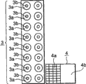
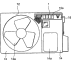
| JP3988720B2 (ja) * | 2003-12-11 | 2007-10-10 | 三菱電機株式会社 | 4方向リードフラットパッケージic実装プリント配線基板及び4方向リードフラットパッケージicの半田付け方法、4方向リードフラットパッケージic実装プリント配線基板を備えた空気調和機。 |
-
2004
- 2004-06-03 JP JP2004165621A patent/JP4222260B2/ja not_active Expired - Fee Related
-
2005
- 2005-04-15 ES ES05252366T patent/ES2401585T3/es not_active Expired - Lifetime
- 2005-04-15 EP EP05252366A patent/EP1603375B1/en not_active Expired - Lifetime
- 2005-05-20 CN CNB2005100728005A patent/CN100475002C/zh not_active Expired - Lifetime
Patent Citations (4)
| Publication number | Priority date | Publication date | Assignee | Title |
|---|---|---|---|---|
| US4835345A (en) * | 1987-09-18 | 1989-05-30 | Compaq Computer Corporation | Printed wiring board having robber pads for excess solder |
| US5243143A (en) * | 1990-11-13 | 1993-09-07 | Compaq Computer Corporation | Solder snap bar |
| US5604333A (en) * | 1994-11-30 | 1997-02-18 | Intel Corporation | Process and structure for a solder thief on circuit boards |
| US6407342B1 (en) * | 1999-03-13 | 2002-06-18 | Samsung Electronics Co., Ltd | Printed circuit board capable of preventing electrical short during soldering process |
Also Published As
| Publication number | Publication date |
|---|---|
| EP1603375A1 (en) | 2005-12-07 |
| EP1603375B1 (en) | 2013-03-06 |
| CN1705428A (zh) | 2005-12-07 |
| JP2005347529A (ja) | 2005-12-15 |
| JP4222260B2 (ja) | 2009-02-12 |
| ES2401585T3 (es) | 2013-04-22 |
Similar Documents
| Publication | Publication Date | Title |
|---|---|---|
| CN100493295C (zh) | 扁平封装ic装配印制线路板及其焊接方法、空气调节器 | |
| EP1542517B1 (en) | Printed Circuit Board for Mounting a Quad Flat Package IC, Method of Soldering a Quad Flat Package IC, and Air Conditioning Apparatus with such a Printed Circuit Board | |
| CN102595784B (zh) | 印刷布线基板、四边引线扁平封装ic的焊接方法以及空气调节器 | |
| CN100475002C (zh) | 印刷布线基板及锡焊方法以及装配有印刷布线基板的空调器 | |
| US20050284656A1 (en) | Method for manufacturing printed circuit board and printed circuit board with gas venting hole | |
| CN1929717B (zh) | 导线型电子器件安装印刷电路基板、导线型电子器件的软钎焊方法、空气调节器 | |
| EP2219427B1 (en) | Dual inline lead-type electronic-part-mounted printed circuit board, method of soldering dual inline lead-type electronic part, and air-conditioner | |
| CN101453836B (zh) | 印刷线路板、空调机、印刷线路板的钎焊方法 | |
| JP2009283983A (ja) | プリント配線基板、空気調和機、プリント配線基板の半田付け方法 | |
| JPH09181424A (ja) | 電子部品、プリント配線板及びプリント配線板の製造方法 | |
| JP2004207421A (ja) | ジャンパ線のはんだ付け方法 |
Legal Events
| Date | Code | Title | Description |
|---|---|---|---|
| C06 | Publication | ||
| PB01 | Publication | ||
| C10 | Entry into substantive examination | ||
| SE01 | Entry into force of request for substantive examination | ||
| C14 | Grant of patent or utility model | ||
| GR01 | Patent grant | ||
| CX01 | Expiry of patent term | ||
| CX01 | Expiry of patent term |
Granted publication date: 20090401 |