WO2024247461A1 - 凹部構造を有する部材を製造する方法および凹部構造を有する部材 - Google Patents
凹部構造を有する部材を製造する方法および凹部構造を有する部材 Download PDFInfo
- Publication number
- WO2024247461A1 WO2024247461A1 PCT/JP2024/012084 JP2024012084W WO2024247461A1 WO 2024247461 A1 WO2024247461 A1 WO 2024247461A1 JP 2024012084 W JP2024012084 W JP 2024012084W WO 2024247461 A1 WO2024247461 A1 WO 2024247461A1
- Authority
- WO
- WIPO (PCT)
- Prior art keywords
- recess structure
- group
- cross
- catalytic material
- workpiece
- Prior art date
- Legal status (The legal status is an assumption and is not a legal conclusion. Google has not performed a legal analysis and makes no representation as to the accuracy of the status listed.)
- Ceased
Links
Images








Classifications
-
- H—ELECTRICITY
- H10—SEMICONDUCTOR DEVICES; ELECTRIC SOLID-STATE DEVICES NOT OTHERWISE PROVIDED FOR
- H10P—GENERIC PROCESSES OR APPARATUS FOR THE MANUFACTURE OR TREATMENT OF DEVICES COVERED BY CLASS H10
- H10P50/00—Etching of wafers, substrates or parts of devices
- H10P50/20—Dry etching; Plasma etching; Reactive-ion etching
- H10P50/28—Dry etching; Plasma etching; Reactive-ion etching of insulating materials
- H10P50/282—Dry etching; Plasma etching; Reactive-ion etching of insulating materials of inorganic materials
- H10P50/283—Dry etching; Plasma etching; Reactive-ion etching of insulating materials of inorganic materials by chemical means
-
- G—PHYSICS
- G03—PHOTOGRAPHY; CINEMATOGRAPHY; ANALOGOUS TECHNIQUES USING WAVES OTHER THAN OPTICAL WAVES; ELECTROGRAPHY; HOLOGRAPHY
- G03F—PHOTOMECHANICAL PRODUCTION OF TEXTURED OR PATTERNED SURFACES, e.g. FOR PRINTING, FOR PROCESSING OF SEMICONDUCTOR DEVICES; MATERIALS THEREFOR; ORIGINALS THEREFOR; APPARATUS SPECIALLY ADAPTED THEREFOR
- G03F7/00—Photomechanical, e.g. photolithographic, production of textured or patterned surfaces, e.g. printing surfaces; Materials therefor, e.g. comprising photoresists; Apparatus specially adapted therefor
- G03F7/004—Photosensitive materials
- G03F7/038—Macromolecular compounds which are rendered insoluble or differentially wettable
-
- G—PHYSICS
- G03—PHOTOGRAPHY; CINEMATOGRAPHY; ANALOGOUS TECHNIQUES USING WAVES OTHER THAN OPTICAL WAVES; ELECTROGRAPHY; HOLOGRAPHY
- G03F—PHOTOMECHANICAL PRODUCTION OF TEXTURED OR PATTERNED SURFACES, e.g. FOR PRINTING, FOR PROCESSING OF SEMICONDUCTOR DEVICES; MATERIALS THEREFOR; ORIGINALS THEREFOR; APPARATUS SPECIALLY ADAPTED THEREFOR
- G03F7/00—Photomechanical, e.g. photolithographic, production of textured or patterned surfaces, e.g. printing surfaces; Materials therefor, e.g. comprising photoresists; Apparatus specially adapted therefor
- G03F7/16—Coating processes; Apparatus therefor
- G03F7/162—Coating on a rotating support, e.g. using a whirler or a spinner
-
- G—PHYSICS
- G03—PHOTOGRAPHY; CINEMATOGRAPHY; ANALOGOUS TECHNIQUES USING WAVES OTHER THAN OPTICAL WAVES; ELECTROGRAPHY; HOLOGRAPHY
- G03F—PHOTOMECHANICAL PRODUCTION OF TEXTURED OR PATTERNED SURFACES, e.g. FOR PRINTING, FOR PROCESSING OF SEMICONDUCTOR DEVICES; MATERIALS THEREFOR; ORIGINALS THEREFOR; APPARATUS SPECIALLY ADAPTED THEREFOR
- G03F7/00—Photomechanical, e.g. photolithographic, production of textured or patterned surfaces, e.g. printing surfaces; Materials therefor, e.g. comprising photoresists; Apparatus specially adapted therefor
- G03F7/20—Exposure; Apparatus therefor
- G03F7/2002—Exposure; Apparatus therefor with visible light or UV light, through an original having an opaque pattern on a transparent support, e.g. film printing, projection printing; by reflection of visible or UV light from an original such as a printed image
- G03F7/2004—Exposure; Apparatus therefor with visible light or UV light, through an original having an opaque pattern on a transparent support, e.g. film printing, projection printing; by reflection of visible or UV light from an original such as a printed image characterised by the use of a particular light source, e.g. fluorescent lamps or deep UV light
-
- H—ELECTRICITY
- H10—SEMICONDUCTOR DEVICES; ELECTRIC SOLID-STATE DEVICES NOT OTHERWISE PROVIDED FOR
- H10P—GENERIC PROCESSES OR APPARATUS FOR THE MANUFACTURE OR TREATMENT OF DEVICES COVERED BY CLASS H10
- H10P50/00—Etching of wafers, substrates or parts of devices
Definitions
- the present invention relates to a method for manufacturing a component having a recessed structure and a component having a recessed structure.
- microfabrication technology that can form minute recessed structures on the surface of a sample.
- Various methods have been proposed and put to practical use as microfabrication technology.
- One of the microfabrication techniques is dry etching, in which reactants such as reactive gases, ions, and/or radicals are used to etch the surface of a sample.
- RIE reactive ion etching
- ICP-RIE Inductively coupled reactive ion etching
- ICP-RIE Inductive Coupled Plasma-RIE
- Patent Document 1 describes a method for manufacturing a recess structure in which the extension axis is inclined obliquely with respect to the perpendicular line to the surface of the workpiece by the aforementioned RIE method.
- etching occurs preferentially on the opening side of the recess structure rather than on the bottom surface.
- the recess structure tends to be wider near the opening, making it difficult to form a recess structure with a uniform width dimension along the depth direction with high precision.
- the RIE method simultaneously etches the mask material placed on top of the workpiece. Since the cross section of the mask material is usually a rectangular or trapezoidal shape, when etching is performed from an oblique direction, the shape of the mask material changes. Therefore, from this point of view, there is also the problem that etching occurs preferentially on the opening side of the recess structure rather than on the bottom surface.
- Patent Document 1 does not easily allow for the formation of a recess structure that has a curved shape along the depth direction.
- the present invention has been made in consideration of the above background, and aims to provide a manufacturing method that can relatively easily form a recess structure that is biased in a predetermined direction in a member. It also aims to provide a member that has such a recess structure.
- a method for manufacturing a component having a recessed structure comprising the steps of: (1) providing a catalytic material in a first region of a first surface of a workpiece, the catalytic material comprising: the first surface is composed of an element having a fluoride boiling point of 550° C.
- the catalytic material includes an organic compound having a polar functional group; a step having a first side having a first height H1 and a second side having a second height H2 opposed to each other when viewed in a cross-section of the catalyst material, i.e., perpendicular to the first surface, where H1>0 ⁇ m, H2 ⁇ 0 ⁇ m, and where the height H1 is greater than the height H2; (2) irradiating the catalyst material with irradiation light including deep ultraviolet light having a wavelength of 380 nm or less; (3) exposing the workpiece to a fluorine-containing gas at 80° C.
- step (3) a recess structure is formed under the first region, and the recess structure has a shape that, in the cross-sectional view, at the center of the first region, is biased toward the second side surface relative to a perpendicular line drawn from the first surface.
- a member having a recess structure on a first surface comprises at least one element selected from the group consisting of B, C, Si, P, S, Ti, V, Cr, Ge, As, Se, Nb, Mo, Tc, Ru, Rh, Sn, Sb, Te, I, Ta, W, Re, Os, Ir, Pt, and Au;
- the recess structure has an opening formed in the first surface, a bottom surface, and a sidewall connecting the opening and the bottom surface;
- the recess structure has a cross-sectional view of the recess structure, i.e., a cross-section perpendicular to the first surface, It has a curved shape, a ratio P2/P1 of a dimension P2 of the bottom surface to a dimension P1 of the opening is in a range of 0.99 or more and less than 1.1;
- a member is provided, the center of the base being offset from the center of the opening relative to an axis extending perpendicular to the first
- the present invention provides a manufacturing method that can relatively easily form a recess structure that is biased in a predetermined direction in a component.
- the present invention also provides a component that has such a recess structure.
- FIG. 2 is a schematic diagram showing a reaction mechanism that may occur on a first surface of a processing target when an organic compound does not have a polar functional group.
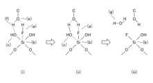
- FIG. 2 is a schematic diagram showing a reaction mechanism that may occur on a first surface of a processing target when an organic compound has a polar functional group.
- FIG. 13 is a schematic diagram showing a reaction mechanism that may occur on a first surface of a processing target when an organic compound has a different polar functional group.
- FIG. 1 is a diagram showing the relationship between the processing temperature and the etching reaction rate during hydrogen fluoride (HF) gas etching of glass.
- HF hydrogen fluoride
- 1 is a cross-sectional view showing a schematic diagram of a process in the "basic etching technique.”
- 1 is a cross-sectional view showing a schematic diagram of a process in the "basic etching technique.”
- 1 is a cross-sectional view showing a schematic state in which a pattern of catalytic material is provided on a first surface of a workpiece in a method according to an embodiment of the present invention;
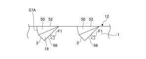
- 3A to 3C are cross-sectional views each showing a schematic state in which etching progresses on a first surface of a processing object in a method according to an embodiment of the present invention.
- FIG. 2 is a cross-sectional view showing an example of a target object after an etching process in a method for producing a member having a recess structure according to an embodiment of the present invention.
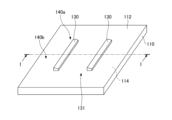
- FIG. 2 is a perspective view of a member according to one embodiment of the present invention.
- 15 is a schematic cross-sectional view taken along line II-II of the member according to the embodiment of the present invention shown in FIG. 14.
- 4A and 4B are diagrams showing the surface morphology of a sidewall of a recess structure in a member according to an embodiment of the present invention;
- FIG. 2 is a schematic diagram illustrating a cross-section of a catalytic material formed in one embodiment of the present invention.
- the conventional RIE method has a problem in that it is difficult to manufacture a member having a recess structure that includes a complex shape along the depth direction.
- the inventors of the present application conducted intensive research and development and discovered a microfabrication technique that can form recessed structures with complex shapes, particularly curved shapes, along the depth direction.
- the basic etching technique involves a process (hereinafter referred to as the "etching process") in which a workpiece having a catalytic material applied to its first surface is exposed to a fluorine-containing gas at a processing temperature of 80°C or higher.
- the basic etching technique makes it possible to selectively etch the area on the first surface of the workpiece where the catalytic material is applied (hereinafter referred to as the "covered area").
- the etching rate in the subsequent etching process is controlled by irradiating a catalytic material with specific irradiation light before performing the etching process on the workpiece.
- the catalytic material comprises an organic compound having a polar functional group, which is believed to play a role in lowering the activation energy of fluoride formation on the surface of the workpiece.
- Figures 1 to 3 show schematic diagrams of the reaction that occurs on the surface of a workpiece on which a catalytic material is placed.
- the Si atoms (b) in order for the Si atoms (b) to react with the F atoms on the surface of the workpiece, the OH groups (c) on the surface must interact with the H atoms of the HF molecules (a) to weaken the H-F bonds, as shown in (ii).
- the Si-F bonds (d) accompanied by the elimination of H 2 O (g) as shown in (iii) do not form.
- Figure 2 shows a schematic diagram of the reaction mechanism on the first surface of the workpiece when the organic compound has a polar functional group.
- the polar functional group is assumed to be a hydroxyl group.
- the O atom in the - ⁇ portion (e) of the polar functional group interacts with the H of the HF molecule (a).
- the H atom in the + ⁇ portion (f) of the polar functional group interacts with the OH group (c) on the surface.
- the H-F bond in the HF molecule (a) is weakened.
- the Si (b)-OH (c) bond is also weakened. This reduces the activation energy required for the bonding reaction between the Si atom and the F atom.
- Both SiF 4 and H 2 O produced by the reaction are in the gaseous state at the treatment temperature and are quickly dispersed outside the system.
- the area directly below the catalytic material coating on the workpiece is selectively etched.
- the above reaction is not limited to cases where the polar functional group contains a hydroxy group.
- a similar reaction may occur when the polar functional group contains at least one of an aldehyde group, a hydroxy group, a carboxy group, an amino group, a sulfo group, a thiol group, and an amide bond.
- Figure 3 shows a schematic of the reaction mechanism when the organic compound has another polar functional group.
- the HF molecule (a) when HF gas is supplied from the environment to the coating area of the catalyst material, the HF molecule (a) undergoes a nucleophilic attack on the Si atom (b), as shown in (i).
- the O atom in the - ⁇ portion (e) of the polar functional group interacts with the H atom of the HF molecule (a).
- reaction formula (1) the reaction shown in reaction formula (1) above occurs, and the area directly below the coated region in the workpiece is selectively etched.
- a similar reaction mechanism can occur, for example, when the polar functional group has at least one of a carbonyl group, a nitro group, a cyano group, an ether bond, and an ester bond.
- the processing temperature is 80°C or higher. This is because, at temperatures below 80°C, proper etching selectivity does not occur between the coated and uncoated areas on the first surface of the workpiece.
- Figure 4 shows the relationship between the processing temperature and the etching reaction rate during hydrogen fluoride (HF) gas etching of glass, as obtained by the inventors of this application.
- This phenomenon is thought to correspond to the associated/non-associated state of HF gas. That is, HF gas is in an associated state below 80°C, but is in a non-associated (single) state above 80°C. Furthermore, when HF gas is in an associated state, the bonding strength of the H-F bond is relatively weaker when viewed as a single molecule. Therefore, the F atoms of the HF molecules are more likely to bond with the surface of the workpiece and form fluorides. It is thought that this behavior is the reason why a high etching rate can be obtained below 80°C.
- the processing temperature is 80°C or higher
- the high etching power of the associated HF gas can be suppressed in the uncoated areas of the catalytic material.
- etching of the treated object becomes possible directly below the coated area.
- high etching selectivity can be obtained between the coated and uncoated areas of the catalytic material. This also makes it possible to selectively etch the coated area using basic etching techniques.
- Figures 5 and 6 show a schematic diagram of one step in the basic etching technique.
- FIG. 5 shows a schematic diagram of a catalyst material 3 placed on the surface of a workpiece 1. Note that in FIGS. 5 and 6, for ease of illustration, the workpiece 1 and the catalyst material 3 are shown spaced apart from each other, but in reality, they are in contact with each other.
- the object 1 to be processed is assumed to be made of SiO 2 and its surface is assumed to be H-terminated.
- the catalytic material 3 is an organic compound having a polar functional group, which is assumed to be an OH group here.
- etching proceeds selectively directly below the coating region 8a where the catalytic material 3 is placed. As a result, a recess structure is formed directly below the coating region 8a.
- FIG. 6 shows the state in which etching of the workpiece 1 has progressed to a certain extent and a recess structure 5 of a certain depth has been formed.
- catalytic material 3 is placed in the covering region 8a. Therefore, even as the etching reaction progresses, catalytic material 3 remains on the bottom surface 6 of the recessed structure 5. In other words, while the etching process continues, the bottom surface 6 of the recessed structure 5 continues to be in contact with catalytic material 3. As a result, the bottom surface 6 of the recessed structure 5 continues to be etched by the reaction mechanism described above, and the bottom surface 6 continues to progress in the depth direction.
- the etching reaction proceeds in the portion of the sidewall 7 that comes into contact with the catalytic material 3 according to the mechanism described above. More precisely, only the portion that comes into contact with the side of the catalytic material 3 of the workpiece 1 is etched. As a result, in the portion that comes into contact with the side of the catalytic material 3, a recess structure 5 defined by the sidewall 7 is formed.
- first sidewall portion 7a such a sidewall 7 that is no longer in contact with the side of the catalyst material 3 is referred to as the "first sidewall portion 7a.”
- etching does not substantially proceed.
- the etching reaction occurs only when the workpiece 1 is in contact with the catalytic material 3, and does not occur in any other state.
- etching virtually stops proceeding thereafter.
- etching of the workpiece 1 proceeds selectively only directly below the catalytic material 3, ultimately forming a vertical recess structure.
- the basic etching technique also includes a step of irradiating the catalytic material with irradiation light containing deep ultraviolet (DUV) rays with a wavelength of 380 nm or less (hereinafter referred to as the "DUV irradiation process") before carrying out the etching process on the workpiece.
- DUV deep ultraviolet
- the etching rate of the treated object can be controlled by performing the etching process after the DUV irradiation process, which is thought to be because the number of polar functional groups changes due to the DUV irradiation process.
- the presence of the catalytic material 3 lowers the reaction barrier in reaction formula (1), and etching proceeds selectively in the coated region 8a during the etching process.
- a crosslinking reaction occurs within the catalyst material 3 as a result of exposure to deep ultraviolet light with a wavelength of 380 nm or less.
- the crosslinking reaction reduces the number of polar functional groups (e.g., C-OH groups) contained in the catalyst material 3.
- polar functional groups e.g., C-OH groups
- the number of polar functional groups contained in the catalytic material 3 also changes by changing the irradiation intensity of the irradiation light including deep ultraviolet light and the irradiation time of the irradiation light in the DUV irradiation process. Therefore, by changing the irradiation conditions in the DUV irradiation process, the etching rate of the workpiece 1 in the etching process can be controlled.
- the irradiation intensity of the irradiation light in the DUV irradiation process may be increased and/or the irradiation time may be extended. This significantly reduces the etching rate in the etching process, making it possible to prevent over-etching of the workpiece.
- the irradiation intensity of the irradiation light in the DUV irradiation process may be weakened and/or the irradiation time may be shortened. This increases the etching rate in the etching process and shortens the processing time.
- the new microfabrication technology developed by the present inventors is based on this "basic etching technology.”
- a method for manufacturing a component having a recessed structure comprising the steps of: (1) providing a catalytic material in a first region of a first surface of a workpiece, the catalytic material comprising: the first surface is composed of an element having a fluoride boiling point of 550° C.
- the catalytic material includes an organic compound having a polar functional group; a step having a first side having a first height H1 and a second side having a second height H2 opposed to each other when viewed in a cross-section of the catalyst material, i.e., perpendicular to the first surface, where H1>0 ⁇ m, H2 ⁇ 0 ⁇ m, and where the height H1 is greater than the height H2; (2) irradiating the catalyst material with irradiation light including deep ultraviolet light having a wavelength of 380 nm or less; (3) exposing the workpiece to a fluorine-containing gas at 80° C.
- step (3) a recess structure is formed under the first region, and the recess structure has a shape that, in the cross-sectional view, at the center of the first region, is biased toward the second side surface relative to a perpendicular line drawn from the first surface.
- the shape biased toward the second side of the recess structure may be a straight line or a curved line.
- the catalytic material placed on the first surface has a first side and a second side that are mutually opposed in a cross-sectional view of the catalytic material, and is characterized in that the height H1 of the first side is greater than the height H2 of the second side (H2 ⁇ 0 ⁇ m).
- cross-sectional view of (the catalytic material) means viewing the target component (e.g., the catalytic material) in a cross section perpendicular to the first surface of the workpiece.
- a recess structure having a shape biased toward the second side surface can be formed in the workpiece.
- Figures 7 to 9 show schematic diagrams of the process of forming a recess structure on a first surface of a workpiece in one embodiment of the present invention.
- FIG. 7 shows a state in which a pattern of catalytic material 3 has been placed on the first surface 12 of the workpiece 1.
- FIG. 8 shows the state after the etching process has started (etching time t1) for the workpiece 1 after the DUV irradiation process.
- FIG. 9 shows the state in which the etching process for the workpiece 1 has progressed further (etching time t2; t2>t1).
- a catalytic material 3 that is triangular in cross section is placed on the first surface 12.
- the catalytic material 3 has a top surface 18 and a bottom surface 19.
- the height of the top surface 18 decreases continuously from a maximum value on the left side of FIG. 7 to a minimum value (zero) on the right side.
- the catalyst material 3 shown in FIG. 7 can also be said to have a configuration in which the first side (left side of FIG. 7) has a first side 17A with a height H1, and the second side 17B with a height H2 on the second side (right side of FIG. 7).
- H2 0. That is, in the present application, H1>0, whereas H2 ⁇ 0.
- the etching speed of the workpiece 1 changes on both sides. In other words, the etching speed is faster on the first side 17A side, which has more polar functional groups, than on the second side 17B side.
- the recessed structure 50 that is formed is deeper directly beneath the first side 17A of the catalytic material 3 than directly beneath the second side 17B, as shown in FIG. 8.
- the recess structure 50 formed has a longer sidewall 57A corresponding to the first side 17A of the catalyst material 3 than a longer sidewall 57B corresponding to the second side 17B.
- the recess structure 50 has a configuration biased toward the second side 17B.
- the recess structure 50 has a non-linear configuration that is curved toward the second side 17B.
- a component can be manufactured that has a recess structure 5 biased in a predetermined direction on the underside of the first surface 12.
- the areas of the bottom surface 56 and the opening 52 of the recess structure 50 are substantially the same at any stage of the etching process.
- the recess structure 50 formed has a characteristic that the width dimension is substantially constant in the cross-sectional view and in the extension direction.
- Figure 10 shows a schematic flow of a method for manufacturing a component having a recessed structure according to one embodiment of the present invention (hereinafter simply referred to as the "first method").
- the first method is as follows: (1) providing a workpiece having a first surface, A step (S110) in which the first surface contains an element having a fluoride boiling point of 550° C. or less; (2) providing a catalytic material in a first region of the first surface of the workpiece, the catalytic material comprising:
- the catalytic material includes an organic compound having a polar functional group;
- the catalytic material has, in a cross-sectional view of the catalytic material, a first side having a first height H1 and a second side having a second height H2 opposed to each other;
- a step (S120) in which a height H1 (H1>0 ⁇ m) of the first side surface is higher than a height H2 (H2 ⁇ 0 ⁇ m) of the second side surface;
- Step S110 First, an object to be processed is prepared.
- the object to be treated may be composed of a single component or multiple components.
- the object to be treated is composed of a single material
- the object to be treated is composed of an element that reacts with fluorine (F) to form a fluoride with a boiling point of 550°C or less.
- the object to be treated may contain at least one element selected from the group consisting of B, C, Si, P, S, Ti, V, Cr, Ge, As, Se, Nb, Mo, Tc, Ru, Rh, Sn, Sb, Te, I, Ta, W, Re, Os, Ir, Pt, and Au.
- the object to be treated may further contain at least one element selected from the group consisting of H, N, Cl, Br, and O.
- the object to be treated is composed of an element that reacts with fluorine to form a fluoride with a boiling point of 200°C or less.
- silicon (Si) has a boiling point of -86°C in the form of fluoride SiF4 , and a workpiece containing silicon can be suitably used as the workpiece in the first method.
- Al and Ca cannot be said to be elements that react with fluorine (F) to form fluorides with a boiling point of 550° C. or lower.
- the workpiece may be, for example, a quartz glass substrate, a quartz substrate, or a silicon substrate.
- the object to be treated is composed of a laminate of multiple components
- the object to be treated contains an element whose fluoride boiling point is 550°C or less on the outermost surface (corresponding to the "first surface” in this application).
- Such elements may be selected from the group consisting of, for example, B, C, Si, P, S, Ti, V, Cr, Ge, As, Se, Nb, Mo, Tc, Ru, Rh, Sn, Sb, Te, I, Ta, W, Re, Os, Ir, Pt, and Au.
- the first surface may further include at least one element selected from the group consisting of H, N, Cl, Br, and O.
- the workpiece may have one or more films disposed on a substrate, with the outermost film satisfying the aforementioned characteristics.
- the entirety of the multiple films may satisfy the aforementioned characteristics.
- Such films may comprise, for example, at least one of SiO 2 , Si 3 N 4 , and SiC.
- the substrate may have the above-mentioned characteristics in addition to the film.
- the first method can be used to manufacture a component in which a recess structure is formed even inside the substrate.
- the substrate may be, for example, a quartz glass substrate, a quartz substrate, or a silicon substrate.
- the workpiece is made of a single piece of quartz glass, and that a recess structure is formed on the first surface of the quartz glass.
- Step S120 Next, a catalytic material is applied to a first surface of the workpiece, the catalytic material being applied to a predetermined area of the first surface.
- the catalyst material includes an organic compound having a polar functional group.
- the polar functional group may include at least one selected from the group consisting of, for example, a hydroxy group, an aldehyde group, a carboxy group, an amino group, a sulfo group, a thiol group, an amide bond, a carbonyl group, a nitro group, a cyano group, an ether bond, and an ester bond.
- Typical examples of such organic compounds include phenolic resins, acrylic resins, and methacrylic resins.
- the catalyst material may consist solely of the organic compound having the aforementioned polar functional groups, or may be provided as a mixture with other additives.
- the catalyst material may include a solvent, a binder, and/or fine particles, etc.
- the method for installing the catalyst material is not particularly limited.
- the catalytic material may be applied to the first surface of the workpiece by, for example, a coating method, a printing method, a spin coating method, or a spraying method.
- Figure 11 shows a schematic diagram of the catalyst material being placed on the workpiece.
- the workpiece 110 has a first surface 112 and a second surface 114.
- the catalytic material 130 is disposed on a portion of the first surface 112 of the workpiece 110.
- the catalytic material 130 is arranged as a pattern 131 of multiple parallel lines. However, this is merely an example, and the catalytic material 130 may be arranged in any manner depending on the required recess structure.
- the catalytic material 130 may be arranged, for example, as a single straight line. Alternatively, the catalytic material 130 may be arranged, for example, as a circular dot pattern or a single circular dot.
- the area of the first surface 112 where the catalyst material 130 is placed is referred to as the coated area 140a, and the other areas are referred to as the non-coated areas 140b.
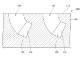
- FIG. 12 shows a schematic diagram of a portion of a cross section taken along line I-I in FIG. 11.
- each catalyst material 130 has a shape with different thicknesses (heights) on the left and right sides in a cross-sectional view.
- each catalyst material 130 has a top surface 118 and a bottom surface 119, and a first side surface 117A and a second side surface 117B of different heights.
- the height H1 of the first side surface 117A is configured to be higher than the height H2 of the second side surface 117B. Therefore, the top surface 118 of the catalyst material 130 has an inclined surface with the second side surface 117B side descending.
- the upper surface 118 of the catalytic material 130 does not necessarily have to be a straight line connecting the top of the first side surface 117A and the top of the second side surface 117B.
- the upper surface 118 of the catalytic material 130 may be non-linear, such as a downwardly convex curved line or an upwardly convex curved line, in a cross-sectional view.
- the upper surface 118 may have one or more steps.
- the catalyst material 130 may have an angle ⁇ (0° ⁇ 90°) between the straight line E connecting the first side 117A and the second side 117B (which coincides with the top surface 118 in the example shown in FIG. 12) and the first surface 112 in a cross-sectional view in the range of 1° to 80°.
- ⁇ is preferably in the range of 3° to 50°, and more preferably in the range of 5° to 15°.
- the width W (see FIG. 12) of the catalyst material 130 is not particularly limited, but is, for example, in the range of 0.1 ⁇ m to 100 ⁇ m, and preferably in the range of 0.3 ⁇ m to 50 ⁇ m.
- the irradiation light includes deep ultraviolet (DUV) light having a wavelength of 380 nm or less.
- the wavelength of deep ultraviolet light may be in the range of 200 nm to 365 nm.
- the illumination light is emitted from a light source.
- a light source may be a light source that emits light of a single wavelength (or a single range of wavelengths) or a light source that emits light of multiple wavelengths (or multiple ranges of wavelengths).
- the irradiation conditions such as the irradiation intensity and irradiation time of the irradiation light, are determined by the etching rate adopted in the subsequent step S140.
- the degree of deflection of the recess structure formed after step S140 is determined by the difference in etching rate caused by the difference in the amount of polar functional groups contained on both sides of the catalytic material (side 17A side and second side 17B side). Therefore, even if the intensity of the DUV irradiation irradiated to the entire surface of the catalytic material is changed, the degree of deflection of the recess structure itself does not change significantly.
- the dose P (mJ/cm 2 ) of the irradiated light may be 20 mJ/cm 2 or more.
- the processing temperature is 80°C or higher.
- the actual processing temperature varies depending on the elements contained in the workpiece 110 (particularly the first surface 112) and the type and depth of the recessed structure, but is usually in the range of 200°C to 450°C, and preferably in the range of 250°C to 400°C.
- the processing temperature By setting the processing temperature at 450°C or lower, it is possible to suppress the deterioration of the organic compounds contained in the catalyst material 130.
- the etching process of the workpiece 110 in such an environment causes the reaction formula (1) described above to occur in the coating region 140a. Furthermore, the fluoride and water produced by the reaction become gas and dissipate outside the system. As a result, a recess structure biased in a predetermined direction is formed in the coating region 140a of the first surface 112.
- FIG. 13 shows a schematic diagram of an example of a cross section of the workpiece 110 after etching.
- a curved recess structure 150 biased to the right may be formed.
- a process may be performed to remove the catalytic material 130 remaining on the bottom surface of the recessed structure 150.
- the catalytic material 130 may be removed by cleaning the workpiece 110 with an acid solution, an alkaline solution, an organic solvent, a corrosive gas, or plasma.
- a component 100 can be manufactured that has a recess structure 150 on the first surface 112 that is biased in a predetermined direction.
- the depth of the recess structure 150 is, for example, 10 ⁇ m or more, and may be 15 ⁇ m or more.
- FIG. 14 shows a perspective view of a member having a recess structure according to one embodiment of the present invention (hereinafter referred to as "first member 300"). Also, FIG. 15 shows a schematic enlarged cross-sectional view of the first member 300 shown in FIG. 14 taken along line II-II.
- the first member 300 has a first surface 302 and a second surface 304 that face each other.
- the first member 300 also has a recess structure 350 on the side of the first surface 302.
- the first surface 302 and the second surface 304 of the first member 300 are substantially rectangular.
- the shapes of the first surface 302 and the second surface 304 are not particularly limited.
- each recess structure 350 is formed on the first surface 302, and the two recess structures 350 are arranged parallel to each other.
- Each recess structure 350 has a linear opening that extends in one direction.
- the recess structure 350 has an opening 352 in the first surface 302.
- the recess structure 350 also has a bottom surface 356 and a sidewall 357.
- the recess structure 350 is defined by the opening 352, the bottom surface 356, and the sidewall 357.
- the recess structure 350 has a shape that is biased in a predetermined direction. Specifically, the side wall 357 of the recess structure 350 does not extend parallel to the vertical direction, but is biased to the right, and the side wall 357 of the recess structure 350 has a curved shape.
- the recess structure 350 has a feature that, when viewed from a cross section perpendicular to the first surface 302 (i.e., in a cross-sectional view), the dimension P1 of the opening 352 (which may be considered to be the area of the opening 352) and the dimension P2 of the bottom surface 356 (which may be considered to be the area of the bottom surface 356) are substantially equal.
- the ratio P2/P1 is equal to or greater than 0.90 and less than 1.1. It is particularly preferable that the ratio P2/P1 is in the range of 0.94 to 1.05.
- Such a first member 300 can be manufactured, for example, by the first method described above.
- the recess structure 350 may have a depth of 10 ⁇ m or more.
- the recess structure 350 may have a form in which the angle ⁇ (0° ⁇ 180°) of the sidewall 357 with respect to a plane parallel to the first surface 302 changes continuously from the opening 352 to the bottom surface 356.
- the angle ⁇ means the angle between the tangent of the sidewall 357 passing through the "outside" of the recess structure 350 and the horizontal plane.
- the angle ⁇ of the sidewall 357 measured at the intersection point between the sidewall 357 and the bottom surface 356 as shown in FIG. 15 is particularly referred to as " ⁇ b .”
- the angle ⁇ b may be any value, for example in the range of 10° to 80°.
- the recess structure 350 may have a curved shape in which it is not possible to connect the center of the opening 352 and the center of the bottom surface 356 in a straight line in a cross-sectional view, as shown in FIG. 21 described below.
- the first member 300 has a feature that the surface constituting the sidewall 357 in the recess structure 350 is relatively smooth and has a surface roughness Ra of 5 nm or less.
- the surface roughness Ra of the sidewall 357 is preferably 4.5 nm or less, and more preferably 4.0 nm or less.
- the coated region 8a is selectively etched by the catalytic material 3 placed on the coated region 8a. Furthermore, as long as the relationship between the catalytic material 3 and the coated region 8a continues, the recess structure 5 continues to progress in the depth direction.
- the sidewall 7 of the recessed structure 5 created by etching is affected by the state of the side of the catalytic material 3 with which the sidewall 7 comes into contact.
- the side surface of the catalyst material 3 is considered to be relatively smooth with few irregularities. Reflecting the influence of the irregularities on the side surface of such catalyst material 3, the side wall 7 of the recess structure 5 also has a relatively smooth surface. As a result, it is considered that the side wall 7 of the recess structure 5 has a surface with significantly reduced surface roughness.
- the first member 300 may also be characterized in that the sidewall 357 has a streak pattern that runs along the extension direction of the recess structure 350.
- FIG. 16 shows a schematic representation of the surface shape of the sidewall 357 of the recess structure 350.
- FIG. 16 also shows a schematic representation of a portion of the surface of the sidewall 357.
- a continuous streak (hereinafter referred to as a "continuous streak") 380 is formed on the side wall 357 of the recess structure 350, which continues from the opening 352 to the bottom surface 356.
- FIG. 16 three continuous streaks 380 are shown. However, this is merely an example, and the number of continuous streaks 380 is not particularly limited.
- the sidewall 7 of the recess structure 5 formed by etching in the basic etching technique is affected by the condition of the side surface of the catalytic material 3 with which the sidewall 7 comes into contact.
- the catalyst material 3 having such irregularities on the side advances along the depth direction of the recess structure 5 to the bottom surface 6 of the recess structure 5. Therefore, a continuous stripe pattern corresponding to such irregularities is easily formed on the side wall 7 of the finally obtained recess structure 5.
- the first member 300 may be a single member or may be made up of multiple members.
- the first member 300 When the first member 300 is composed of a single material, the first member 300 is composed of an element that reacts with fluorine (F) to form a fluoride having a boiling point of 550°C or less.
- F fluorine
- the first member 300 may contain at least one element selected from the group consisting of B, C, Si, P, S, Ti, V, Cr, Ge, As, Se, Nb, Mo, Tc, Ru, Rh, Sn, Sb, Te, I, Ta, W, Re, Os, Ir, Pt, and Au.
- the workpiece may further contain at least one element selected from the group consisting of H, N, Cl, Br, and O.
- the first member 300 When the first member 300 is composed of a single member, the first member 300 may be, for example, a quartz glass substrate or a quartz substrate.
- the first member 300 when the first member 300 is composed of multiple members, the first member 300 contains an element on the first surface 302, the fluoride of which has a boiling point of 550°C or less.
- the first surface 302 may further include at least one element selected from the group consisting of H, N, Cl, Br, and O.
- the first component 300 may have one or more films disposed on a substrate material, with the outermost film satisfying the aforementioned characteristics.
- the entirety of the multiple films may satisfy the aforementioned characteristics.
- Such a film may, for example, comprise at least one of SiO2 , Si3N4 , and SiC.
- the film as well as the substrate material may have the aforementioned characteristics .
- the first member 300 having these characteristics can be used in a variety of applications, such as MEMS devices, microfluidic devices, semiconductor devices, optical devices, metasurface devices, resin molding molds, window glass, and cover glass.
- Example 1 A recess structure was formed on one surface (first surface) of the object to be processed by the following method.
- a quartz glass substrate was prepared as the object to be treated.
- a coating liquid containing a catalyst material was also prepared.
- An i-line resist was used as the catalyst material, and the coating liquid was prepared by mixing this with a solvent (ethyl lactate, n-butyl acetate).
- the i-line resist used contains a novolac resin represented by the following chemical formula:
- the i-line resist has hydroxy groups as polar functional groups.
- the coating liquid was applied to the first surface of the substrate by spin coating.
- a line pattern of catalytic material was then deposited on the first surface of the substrate using a grayscale exposure and subsequent development process.
- Figure 17 shows a schematic cross-section of the formed catalyst material.
- the catalytic material 430 has a rectangular cross section that resembles a trapezoid rotated 90 degrees. That is, the catalytic material 430 has a first side 417A and a second side 417B that face each other, and a top surface 418.
- the height H1 of the first side 417A is approximately 1.0 ⁇ m, and the height H2 of the second side 417B is approximately 0.5 ⁇ m.
- the inclination angle of the upper surface 418 i.e., the angle ⁇ r, is 2.9°.
- the catalyst material was irradiated with light using a low-pressure mercury lamp (hereinafter referred to as "Lamp A").
- Lamp A was a DUV lamp with a dominant wavelength of 254 nm, and the dose P of irradiation to the catalyst material was set to 72000 mJ/cm 2 .
- the processing temperature was 250°C, and the processing time was 40 minutes.
- Example 1 After the etching process, a recessed structure was formed on the surface.
- the resulting treated object is referred to as "Sample 1.”
- Example 2 A recess structure was formed on the first surface of the substrate by the same method as in Example 1. However, in Example 2, the shape of the catalyst material was changed from that in Example 1 to form the recess structure. Specifically, in Fig. 17, the inclination angle ⁇ r of the upper surface 418 was set to 5.7°, and the height H2 of the second side surface 417B was set to 0. Therefore, the cross section of the catalyst material was triangular.
- Example 2 After the etching process, a recessed structure was formed on the surface.
- the resulting treated object is referred to as "Sample 2.”
- Example 3 A recess structure was formed on the first surface of the substrate by the same method as in Example 2. However, in Example 3, unlike Example 2, the dose of the irradiated light was set to 144,000 mJ/cm 2 .
- Example 3 After the etching process, a recessed structure was formed on the surface.
- the resulting treated object is referred to as "Sample 3.”
- Example 4 A recess structure was formed on the first surface of the substrate by the same method as in Example 1. However, in Example 4, the shape of the catalyst material was changed from that in Example 1 to form the recess structure. Specifically, in FIG. 17, the inclination angle ⁇ r of the upper surface 418 was set to 11.3°, and the height H2 of the second side surface 417B was set to 0. Therefore, the cross section of the catalyst material was triangular. The width of the catalyst material was 5 ⁇ m.
- Example 4 the amount of irradiation light P was changed from that in Example 1 to form the recessed structure.
- Example 4 After the etching process, a recessed structure was formed on the surface.
- the resulting treated object is referred to as "Sample 4.”
- Table 1 summarizes the preparation conditions and evaluation results for each sample.
- a method for manufacturing a component having a recessed structure comprising the steps of: (1) providing a catalytic material in a first region of a first surface of a workpiece, the catalytic material comprising: the first surface is composed of an element having a fluoride boiling point of 550° C.
- the catalytic material includes an organic compound having a polar functional group; a step having a first side having a first height H1 and a second side having a second height H2 opposed to each other when viewed in a cross-section of the catalyst material, i.e., perpendicular to the first surface, where H1>0 ⁇ m, H2 ⁇ 0 ⁇ m, and where the height H1 is greater than the height H2; (2) irradiating the catalyst material with irradiation light including deep ultraviolet light having a wavelength of 380 nm or less; (3) exposing the workpiece to a fluorine-containing gas at 80° C.
- step (3) having A method in which, after step (3), a recess structure is formed under the first region, and the recess structure has a shape that, in the cross-sectional view, at the center of the first region, is biased toward the second side surface relative to a perpendicular line drawn from the first surface.
- Aspect 4 The method of any one of aspects 1 to 3, wherein the catalytic material has an upper surface that, in the cross-section, monotonically decreases in height from the first side to the second side.
- the polar functional group includes at least one selected from the group consisting of a hydroxy group, an aldehyde group, a carboxy group, an amino group, a sulfo group, a thiol group, an amide bond, a carbonyl group, a nitro group, a cyano group, an ether bond, and an ester bond.
- the first surface comprises at least one element selected from the group consisting of H, B, C, N, O, Si, P, S, Cl, Ti, V, Cr, Ge, As, Se, Br, Nb, Mo, Tc, Ru, Rh, Sn, Sb, Te, I, Ta, W, Re, Os, Ir, Pt, and Au.
- a member having a recess structure on a first surface comprises at least one element selected from the group consisting of B, C, Si, P, S, Ti, V, Cr, Ge, As, Se, Nb, Mo, Tc, Ru, Rh, Sn, Sb, Te, I, Ta, W, Re, Os, Ir, Pt, and Au;
- the recess structure has an opening formed in the first surface, a bottom surface, and a sidewall connecting the opening and the bottom surface;
- the recess structure has a cross-sectional view of the recess structure, i.e., a cross-section perpendicular to the first surface, It has a curved shape, a ratio P2/P1 of a dimension P2 of the bottom surface to a dimension P1 of the opening is in a range of 0.99 or more and less than 1.1;
- the center of the bottom surface is offset from the center of the opening relative to an axis extending perpendicular to the first surface.
- Aspect 19 The article of any of aspects 13-18, wherein the article comprises a substrate and a membrane disposed on the substrate, the membrane comprising at least one of SiO2 , SiN, and SiC, forming the first surface.
Landscapes
- Physics & Mathematics (AREA)
- General Physics & Mathematics (AREA)
- Spectroscopy & Molecular Physics (AREA)
- Surface Treatment Of Glass (AREA)
- Catalysts (AREA)
Priority Applications (3)
| Application Number | Priority Date | Filing Date | Title |
|---|---|---|---|
| JP2025523297A JPWO2024247461A1 (https=) | 2023-05-31 | 2024-03-26 | |
| CN202480035726.0A CN121219816A (zh) | 2023-05-31 | 2024-03-26 | 制造具有凹部结构的部件的方法和具有凹部结构的部件 |
| US19/385,936 US20260063997A1 (en) | 2023-05-31 | 2025-11-11 | Method for manufacturing member with recess structure and member with recess structure |
Applications Claiming Priority (2)
| Application Number | Priority Date | Filing Date | Title |
|---|---|---|---|
| JP2023089319 | 2023-05-31 | ||
| JP2023-089319 | 2023-05-31 |
Related Child Applications (1)
| Application Number | Title | Priority Date | Filing Date |
|---|---|---|---|
| US19/385,936 Continuation US20260063997A1 (en) | 2023-05-31 | 2025-11-11 | Method for manufacturing member with recess structure and member with recess structure |
Publications (1)
| Publication Number | Publication Date |
|---|---|
| WO2024247461A1 true WO2024247461A1 (ja) | 2024-12-05 |
Family
ID=93657139
Family Applications (1)
| Application Number | Title | Priority Date | Filing Date |
|---|---|---|---|
| PCT/JP2024/012084 Ceased WO2024247461A1 (ja) | 2023-05-31 | 2024-03-26 | 凹部構造を有する部材を製造する方法および凹部構造を有する部材 |
Country Status (5)
| Country | Link |
|---|---|
| US (1) | US20260063997A1 (https=) |
| JP (1) | JPWO2024247461A1 (https=) |
| CN (1) | CN121219816A (https=) |
| TW (1) | TW202514768A (https=) |
| WO (1) | WO2024247461A1 (https=) |
Citations (6)
| Publication number | Priority date | Publication date | Assignee | Title |
|---|---|---|---|---|
| JPS531198A (en) * | 1976-05-14 | 1978-01-07 | Int Plasma Corp | Method of etching silicon dioxide |
| JPS5587436A (en) * | 1978-12-25 | 1980-07-02 | Fujitsu Ltd | Method of producing semiconductor device |
| JP2000058508A (ja) * | 1998-08-12 | 2000-02-25 | Seiko Epson Corp | ドライエッチング方法及び装置 |
| WO2006051727A1 (ja) * | 2004-11-09 | 2006-05-18 | Osaka University | 結晶基板に孔を形成する方法、及びその方法で孔が形成された結晶基板 |
| JP2014045030A (ja) * | 2012-08-24 | 2014-03-13 | Osaka Univ | 結晶基板に孔を形成する方法、並びに結晶基板内に配線や配管を有する機能性デバイス |
| JP2022127461A (ja) * | 2021-02-19 | 2022-08-31 | Agc株式会社 | 凹部を有するケイ素含有部材の製造方法 |
-
2024
- 2024-03-26 CN CN202480035726.0A patent/CN121219816A/zh active Pending
- 2024-03-26 WO PCT/JP2024/012084 patent/WO2024247461A1/ja not_active Ceased
- 2024-03-26 JP JP2025523297A patent/JPWO2024247461A1/ja active Pending
- 2024-04-01 TW TW113112268A patent/TW202514768A/zh unknown
-
2025
- 2025-11-11 US US19/385,936 patent/US20260063997A1/en active Pending
Patent Citations (6)
| Publication number | Priority date | Publication date | Assignee | Title |
|---|---|---|---|---|
| JPS531198A (en) * | 1976-05-14 | 1978-01-07 | Int Plasma Corp | Method of etching silicon dioxide |
| JPS5587436A (en) * | 1978-12-25 | 1980-07-02 | Fujitsu Ltd | Method of producing semiconductor device |
| JP2000058508A (ja) * | 1998-08-12 | 2000-02-25 | Seiko Epson Corp | ドライエッチング方法及び装置 |
| WO2006051727A1 (ja) * | 2004-11-09 | 2006-05-18 | Osaka University | 結晶基板に孔を形成する方法、及びその方法で孔が形成された結晶基板 |
| JP2014045030A (ja) * | 2012-08-24 | 2014-03-13 | Osaka Univ | 結晶基板に孔を形成する方法、並びに結晶基板内に配線や配管を有する機能性デバイス |
| JP2022127461A (ja) * | 2021-02-19 | 2022-08-31 | Agc株式会社 | 凹部を有するケイ素含有部材の製造方法 |
Also Published As
| Publication number | Publication date |
|---|---|
| US20260063997A1 (en) | 2026-03-05 |
| CN121219816A (zh) | 2025-12-26 |
| JPWO2024247461A1 (https=) | 2024-12-05 |
| TW202514768A (zh) | 2025-04-01 |
Similar Documents
| Publication | Publication Date | Title |
|---|---|---|
| US8361339B2 (en) | Antireflection structure formation method and antireflection structure | |
| WO2023119899A1 (ja) | 凹部構造を有する部材を製造する方法、および凹部構造を有する部材 | |
| JP5264237B2 (ja) | ナノ構造体およびナノ構造体の製造方法 | |
| US9927692B2 (en) | Reflective photomask and production method therefor | |
| JP2006013216A (ja) | 近接場露光によるレジストパターンの形成方法、及び該レジストパターンの形成方法を用いた基板の加工方法、デバイスの作製方法 | |
| TWI646598B (zh) | Microscopic three-dimensional structure forming method and microscopic three-dimensional structure | |
| TW202136013A (zh) | 覆板及製造覆板之方法 | |
| US20250215319A1 (en) | Method for manufacturing member with recess structure and member with recess structure | |
| US20070287100A1 (en) | Near-field exposure method | |
| WO2024247461A1 (ja) | 凹部構造を有する部材を製造する方法および凹部構造を有する部材 | |
| JP3859473B2 (ja) | スタンパの製造方法 | |
| JP2024066972A (ja) | 凹部構造を有する部材を製造する方法および凹部構造を有する部材 | |
| KR20130039477A (ko) | 나노렌즈어레이몰드의 제조방법 및 그 방법에 의해 제조된 몰드를 이용한 나노렌즈어레이의 제조방법 | |
| JP7526547B2 (ja) | マスクブランク、モールド用マスクブランクの製造方法、及びインプリントモールドの製造方法 | |
| JP4899638B2 (ja) | モールドの製造方法 | |
| JP6097028B2 (ja) | モールドの製造方法及びレジストパターンの形成方法 | |
| WO2012133187A1 (ja) | ナノインプリント用モールドの製造方法および基板作製方法 | |
| US12498643B2 (en) | Fabrication of microscale structures | |
| WO2026005055A1 (ja) | 凹部構造を有する部材を製造する方法 | |
| CN100483158C (zh) | 湿法侧向导引微透镜成形方法 | |
| Li et al. | Bulk Silicon Microfabrication Technology | |
| JP2005114973A (ja) | 微細レジストパターンの形成方法 | |
| KR101367662B1 (ko) | 임프린트용 스탬프 제조 방법 | |
| CN119330300A (zh) | 一种微悬浮结构的制造方法 | |
| JP2017080820A (ja) | 流体デバイスの製造方法および流体デバイス |
Legal Events
| Date | Code | Title | Description |
|---|---|---|---|
| 121 | Ep: the epo has been informed by wipo that ep was designated in this application |
Ref document number: 24814948 Country of ref document: EP Kind code of ref document: A1 |
|
| ENP | Entry into the national phase |
Ref document number: 2025523297 Country of ref document: JP Kind code of ref document: A |
|
| NENP | Non-entry into the national phase |
Ref country code: DE |