WO2024247230A1 - 半導体光電極の製造方法 - Google Patents
半導体光電極の製造方法 Download PDFInfo
- Publication number
- WO2024247230A1 WO2024247230A1 PCT/JP2023/020524 JP2023020524W WO2024247230A1 WO 2024247230 A1 WO2024247230 A1 WO 2024247230A1 JP 2023020524 W JP2023020524 W JP 2023020524W WO 2024247230 A1 WO2024247230 A1 WO 2024247230A1
- Authority
- WO
- WIPO (PCT)
- Prior art keywords
- thin film
- semiconductor thin
- gallium nitride
- semiconductor
- film
- Prior art date
- Legal status (The legal status is an assumption and is not a legal conclusion. Google has not performed a legal analysis and makes no representation as to the accuracy of the status listed.)
- Ceased
Links
Images

Classifications
-
- Y—GENERAL TAGGING OF NEW TECHNOLOGICAL DEVELOPMENTS; GENERAL TAGGING OF CROSS-SECTIONAL TECHNOLOGIES SPANNING OVER SEVERAL SECTIONS OF THE IPC; TECHNICAL SUBJECTS COVERED BY FORMER USPC CROSS-REFERENCE ART COLLECTIONS [XRACs] AND DIGESTS
- Y02—TECHNOLOGIES OR APPLICATIONS FOR MITIGATION OR ADAPTATION AGAINST CLIMATE CHANGE
- Y02P—CLIMATE CHANGE MITIGATION TECHNOLOGIES IN THE PRODUCTION OR PROCESSING OF GOODS
- Y02P70/00—Climate change mitigation technologies in the production process for final industrial or consumer products
- Y02P70/50—Manufacturing or production processes characterised by the final manufactured product
Definitions
- This disclosure relates to a method for manufacturing a semiconductor photoelectrode.
- Non-Patent Document 1 There is a device that produces hydrogen through a water decomposition reaction using a semiconductor photoelectrode (Non-Patent Document 1).
- This device has an oxidation tank and a reduction tank. An aqueous solution and an oxidation electrode are placed in the oxidation tank. An aqueous solution and a reduction electrode are placed in the reduction tank. The oxidation tank and reduction tank are connected via a proton exchange membrane. The oxidation electrode and reduction electrode are electrically connected by a conductor.
- the water splitting reaction using photocatalysts consists of a water oxidation reaction and a proton reduction reaction.
- light is irradiated onto an n-type photocatalyst material, electrons and holes are generated and separated in the photocatalyst.
- the holes move to the surface of the photocatalyst material and contribute to the water oxidation reaction.
- the electrons move to the reduction electrode and contribute to the proton reduction reaction.
- this type of oxidation-reduction reaction progresses, resulting in a water splitting reaction.
- the oxidation electrode is a semiconductor thin film.
- the oxidation electrode is a gallium nitride thin film grown on a sapphire substrate.
- the gallium nitride thin film is irradiated with light in an aqueous solution, the target water oxidation reaction occurs on the gallium nitride surface, and a side reaction, an etching reaction of gallium nitride (GaN), occurs.
- GaN gallium nitride
- a structure can be considered in which a protective layer is formed on the gallium nitride thin film to prevent contact between the aqueous solution and the gallium nitride thin film as much as possible and suppress the etching reaction. If the protective layer is made thicker, light transmission will be hindered according to the thickness of the protective layer. It is preferable that the thickness of the protective layer is as thin as possible, such as approximately 5 nm or less.
- Indium gallium nitride thin films with a high indium composition have a large surface roughness. When the surface roughness exceeds a few nm, it can be difficult to uniformly coat the surface with an extremely thin protective layer.
- This disclosure provides a technology that can reduce the roughness of indium gallium nitride thin films.
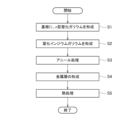
- FIG. 1 is a flowchart showing an example of a method for manufacturing a semiconductor photoelectrode according to the present disclosure.
- FIG. 2 is a cross-sectional view showing an example of the configuration of a semiconductor photoelectrode according to the present disclosure.
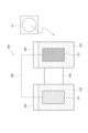
- FIG. 3 is a diagram showing an outline of an apparatus for carrying out an oxidation-reduction reaction test.
- the device 100 includes a light source 101, an oxidation tank 102, a reduction tank 103, a proton exchange membrane 104, and a lead wire 106.
- the oxidation tank 102 includes an oxidation electrode 121 and an aqueous solution 122.
- the oxidation tank 102 is provided with a light receiving window 124.
- the light receiving window 124 receives light from the light source 101 to the oxidation electrode 121.
- the reduction tank 103 includes a reduction electrode 131 and an aqueous solution 132.
- the oxidation electrode 121 is in contact with the aqueous solution 122.
- the oxidation electrode 121 is a nitride semiconductor, titanium oxide, amorphous silicon, or the like.
- the aqueous solution 122 is, for example, an aqueous sodium hydroxide solution, an aqueous potassium hydroxide solution, or hydrochloric acid.
- the reduction electrode 131 is in contact with the aqueous solution 132.
- the reduction electrode 131 is a metal or a metal compound, such as nickel, iron, gold, platinum, silver, copper, indium, or titanium.
- the aqueous solution 132 is, for example, an aqueous solution of potassium bicarbonate, sodium bicarbonate, potassium chloride, or sodium chloride.
- the proton exchange membrane 104 is sandwiched between the oxidation chamber 102 and the reduction chamber 103. Protons are generated in the oxidation chamber 102. The generated protons diffuse into the reduction chamber 103 via the proton exchange membrane 104.
- the proton exchange membrane 104 is, for example, a perfluorocarbon material. Purple carbon material is composed of a hydrophobic Teflon (registered trademark) skeleton made of carbon and fluorine, and perfluoro side chains with sulfonic acid groups.
- the proton exchange membrane 104 is, for example, Nafion (registered trademark).
- the oxidation electrode 121 and the reduction electrode 131 are electrically connected by a conductor 106. Electrons move from the oxidation electrode 121 to the reduction electrode 131 via the conductor 106.
- the light source 101 is, for example, a xenon lamp, a mercury lamp, a halogen lamp, a pseudo-sun light source, sunlight, or a combination of these.
- the light source 101 irradiates light with a wavelength that can be absorbed by the material that constitutes the oxide electrode 121.
- the wavelength that can be absorbed by the oxide electrode 121 is 365 nm or less.
- the oxidation electrode 121 is, for example, a gallium nitride thin film grown on a sapphire substrate.
- the gallium nitride thin film is irradiated with light in an aqueous solution, the target water oxidation reaction occurs on the gallium nitride surface, and a side reaction, an etching reaction of gallium nitride (GaN), occurs.
- GaN gallium nitride
- a structure can be considered in which a protective layer is formed on the gallium nitride thin film to prevent contact between the aqueous solution and the gallium nitride thin film as much as possible and suppress the etching reaction.
- the protective layer it is preferable for the protective layer to be as thin as possible, such as less than about 5 nm.
- indium gallium nitride thin films with a high indium composition are expected to achieve high efficiency by responding to visible light.
- the manufacturing method of the semiconductor photoelectrode disclosed herein forms an indium gallium nitride thin film with a high indium composition into a high-quality thin film. This makes it possible to form an extremely thin and uniform protective layer on the indium gallium nitride thin film. Furthermore, by forming an extremely thin and uniform protective layer on the indium gallium nitride thin film, it becomes possible to extend the life of the solar energy conversion efficiency.
- step S1 a first semiconductor thin film 12 of n-type gallium nitride is formed on a substrate 11.
- a second semiconductor thin film 13 of indium gallium nitride is grown on the surface of the first semiconductor thin film 12 formed in step S1.
- the processes in steps S1 and S2 are performed by metal organic chemical vapor deposition (MOCVD).
- Step S3 is performed in a nitrogen atmosphere furnace, an ammonia atmosphere furnace, or an MOCVD growth furnace.
- the annealing is preferably performed at a temperature in the range of 700°C to 1100°C for 1 to 30 minutes.
- a metal layer 14 is formed as a protective layer on the surface of the second semiconductor thin film 13 after the annealing process in step S3.
- Step S4 is performed by physical vapor deposition such as vacuum deposition or sputtering, chemical vapor deposition such as metalorganic vapor phase epitaxy, or liquid phase epitaxy.
- nickel (Ni) is used for the metal layer, but this is not limited to this.
- the metal layer may be made of one or more metals selected from nickel, cobalt (Co), copper (Cu), tungsten (W), tantalum (Ta), palladium (Pd), ruthenium (Ru), iron (Fe), zinc (Zn), and niobium (Nb).
- the film thickness is 1 nm to 10 nm. A film thickness of 1 nm to 3 nm is particularly desirable, as it allows sufficient light transmission.
- step S5 the semiconductor thin film on which the metal layer has been formed in step S4 is heat-treated.
- the heat treatment is performed on a hot plate, but this is not limited to this.
- the heat treatment may also be performed in an electric furnace.
- the heat treatment atmosphere is air, but it may also be an oxygen atmosphere.
- the aqueous solution used in the oxidation-reduction reaction test below may be an aqueous potassium hydroxide solution or hydrochloric acid in addition to sodium hydroxide.
- the aqueous solution 132 in the reduction tank 103 may be an aqueous sodium hydrogen carbonate solution, an aqueous potassium chloride solution, or an aqueous sodium chloride solution in addition to potassium hydrogen carbonate.
- the target product is hydrogen, but this is not limited to this.
- the reduction electrode can be changed to, for example, Ni, Fe, Au, Pt, Ag, Cu, In, Ti, Co, or Ru.
- Example 1 In Example 1, an n-GaN substrate was used as the substrate. A silicon-doped n-GaN semiconductor thin film was epitaxially grown on a 2-inch n-GaN substrate by MOCVD. Ammonia gas and trimethylgallium were used as growth materials. Silane gas was used as the n-type impurity source. Hydrogen was used as the carrier gas sent into the growth furnace. The thickness of the n-GaN film was 2 ⁇ m, which is sufficient to absorb light. The carrier density was 3 ⁇ 1018 cm-3.
- indium gallium nitride InGaN with an indium composition ratio of 10% was grown.
- Ammonia gas, trimethylgallium, and trimethylindium were used as growth materials.
- Hydrogen was used as the carrier gas sent into the growth furnace.
- the film thickness was set to 500 nm, which is sufficient to absorb light.
- the film was then annealed by exposing it to a temperature of 700°C for 1 minute in an ammonia atmosphere in the growth furnace. The film was then removed from the furnace, and the 2-inch semiconductor thin film was cleaved into four equal pieces, one of which was used to fabricate an electrode.
- the surface was observed with an atomic force microscope (AFM). The average arithmetic roughness of the surface was less than 1 nm.
- Ni was vacuum-deposited onto the semiconductor thin film to a thickness of 1 nm.
- the film was then placed on a hot plate set at 300°C and heat-treated in air for 1 hour to form a NiO protective layer.
- the cross section of the sample was observed with a transmission electron microscope (TEM).
- TEM transmission electron microscope
- ⁇ Oxidation-reduction reaction test> A conducting wire was connected to a part of the exposed n-GaN surface and soldered using In. After that, it was covered with epoxy resin so that the indium surface would not be exposed. This was installed as the oxidation electrode 121 in FIG. 3.
- the aqueous solution 122 in the oxidation layer was a 1 mol/l aqueous solution of sodium hydroxide.
- the aqueous solution 132 in the reduction tank 103 was a 0.5 mol/l aqueous solution of potassium bicarbonate.
- the reduction electrode 131 was made of platinum (manufactured by Nilaco).
- the proton exchange membrane 104 was made of Nafion (registered trademark).
- Nitrogen gas was flowed in each reaction tank at 10 ml/min.
- the light irradiation area of the oxidation electrode 121 was set to 1 cm2 .
- the aqueous solution was stirred at the center of the bottom of each reaction tank using a stirrer and a stirrer at a rotation speed of 250 rpm.
- the light source 101 was fixed so that it faced the surface of the semiconductor photoelectrode prepared by the above-mentioned procedure on which the NiO protective layer was formed.
- a 300W high-pressure xenon lamp (illuminance 5mW/ cm2 ) was used as the light source 101 to uniformly irradiate the semiconductor photoelectrode with light.
- gas in each reaction tank was collected and the reaction products were analyzed by gas chromatography. As a result, it was confirmed that oxygen was generated in the oxidation tank 102 and hydrogen was generated in the reduction tank 103.
- Example 2 After the film was formed, the film was annealed in a furnace at a temperature of 800° C. for 1 minute. The subsequent steps were the same as in Example 1. When the surface was observed with an AFM, the average arithmetic roughness of the surface was 1 nm or less.
- Example 3 After the film was formed, the film was annealed in a furnace at a temperature of 900° C. for 1 minute. The subsequent steps were the same as in Example 1. When the surface was observed with an AFM, the average arithmetic roughness of the surface was 1 nm or less.
- Example 4 After the film was formed, the film was annealed in a furnace at a temperature of 1000° C. for 1 minute. The subsequent steps were the same as in Example 1. When the surface was observed with an AFM, the average arithmetic roughness of the surface was 1 nm or less.
- Example 5 After the film was formed, the film was annealed in a furnace at a temperature of 1100° C. for 1 minute. The subsequent steps were the same as in Example 1. When the surface was observed with an AFM, the average arithmetic roughness of the surface was 1 nm or less.
- Example 6 After the film was formed, the film was annealed in a furnace at a temperature of 1100° C. for 5 minutes. The subsequent steps were carried out in the same manner as in Example 1. When the surface was observed with an AFM, the average arithmetic roughness of the surface was 1 nm or less.
- Example 7 After the film was formed, the film was annealed in a furnace at a temperature of 1100° C. for 10 minutes. The subsequent steps were the same as in Example 1. When the surface was observed with an AFM, the average arithmetic roughness of the surface was 1 nm or less.
- Example 8 After the film was formed, the film was annealed in a furnace at a temperature of 1100° C. for 30 minutes. The subsequent steps were the same as in Example 1. When the surface was observed with an AFM, the average arithmetic roughness of the surface was 1 nm or less.
- Example 9 After the film was formed, annealing was performed in a nitrogen atmosphere at a temperature of 700° C. for 1 minute. The subsequent steps were performed in the same manner as in Example 1. When the surface was observed with an AFM, the average arithmetic roughness of the surface was 1 nm or less.
- Example 1 After the film was formed, the film was annealed in a furnace at a temperature of 600° C. for 1 minute. The subsequent steps were the same as in Example 1. When the surface was observed with an AFM, the average arithmetic roughness of the surface was about 10 nm.
- Example 2 After the film was formed, the film was annealed in a furnace at a temperature of 600° C. for 30 minutes. The subsequent steps were the same as in Example 1. When the surface was observed with an AFM, the average arithmetic roughness of the surface was about 10 nm.
- Example 4 After the film was formed, the film was annealed in a furnace at a temperature of 1100° C. for 60 minutes. The subsequent steps were the same as in Example 1. When the surface was observed with an AFM, the average arithmetic roughness of the surface was about 15 nm.
- Table 1 shows the amount of hydrogen gas produced versus light exposure time in the examples and comparative examples.
- the amount of each gas produced was normalized by the surface area of the semiconductor photoelectrode. It was found that hydrogen was produced in all cases when exposed to light.
- the amount of hydrogen generated is compared between Examples 1 to 4 and Comparative Examples 1 and 2. There is no significant difference in the amount generated immediately after light irradiation. As time passed from the start of light irradiation, differences in the amount generated were observed. In Comparative Examples 1 and 2, the amount of hydrogen generated was reduced by approximately 30% 100 hours after light irradiation. On the other hand, in Examples 1 to 4, the amount of hydrogen generated was maintained at approximately 10% reduction 100 hours after light irradiation. Compared to Comparative Example 1, Examples 1 to 4, which were annealed at a higher temperature, have improved surface flatness and are thought to have formed a uniform protective layer, thereby suppressing the etching reaction. Furthermore, as in Comparative Example 2, no effect was observed even when the annealing treatment time was extended.
- Example 9 the same effect as in Example 1 was obtained. It is believed that ammonia or nitrogen is preferable as the N source effective for improving the quality of InGaN.
- the manufacturing method of the semiconductor photoelectrode disclosed herein involves growing an indium gallium nitride thin film with a high indium composition, followed by an annealing treatment. This reduces the surface roughness of the semiconductor photoelectrode, making it possible to form an extremely thin and uniform protective layer.
- the manufacturing method of the semiconductor photoelectrode disclosed herein can achieve a long life for solar energy conversion efficiency.
Landscapes
- Photovoltaic Devices (AREA)
Priority Applications (2)
| Application Number | Priority Date | Filing Date | Title |
|---|---|---|---|
| JP2025523173A JPWO2024247230A1 (cg-RX-API-DMAC7.html) | 2023-06-01 | 2023-06-01 | |
| PCT/JP2023/020524 WO2024247230A1 (ja) | 2023-06-01 | 2023-06-01 | 半導体光電極の製造方法 |
Applications Claiming Priority (1)
| Application Number | Priority Date | Filing Date | Title |
|---|---|---|---|
| PCT/JP2023/020524 WO2024247230A1 (ja) | 2023-06-01 | 2023-06-01 | 半導体光電極の製造方法 |
Publications (1)
| Publication Number | Publication Date |
|---|---|
| WO2024247230A1 true WO2024247230A1 (ja) | 2024-12-05 |
Family
ID=93657198
Family Applications (1)
| Application Number | Title | Priority Date | Filing Date |
|---|---|---|---|
| PCT/JP2023/020524 Ceased WO2024247230A1 (ja) | 2023-06-01 | 2023-06-01 | 半導体光電極の製造方法 |
Country Status (2)
| Country | Link |
|---|---|
| JP (1) | JPWO2024247230A1 (cg-RX-API-DMAC7.html) |
| WO (1) | WO2024247230A1 (cg-RX-API-DMAC7.html) |
Citations (3)
| Publication number | Priority date | Publication date | Assignee | Title |
|---|---|---|---|---|
| JP2013084955A (ja) * | 2011-10-07 | 2013-05-09 | Qinghua Univ | 発光ダイオード |
| WO2020116151A1 (ja) * | 2018-12-03 | 2020-06-11 | 日本電信電話株式会社 | 窒化物半導体光電極の製造方法 |
| WO2021236382A1 (en) * | 2020-05-18 | 2021-11-25 | Nanosys, Inc. | Subpixel light emitting diodes for direct view display and methods of making the same |
-
2023
- 2023-06-01 JP JP2025523173A patent/JPWO2024247230A1/ja active Pending
- 2023-06-01 WO PCT/JP2023/020524 patent/WO2024247230A1/ja not_active Ceased
Patent Citations (3)
| Publication number | Priority date | Publication date | Assignee | Title |
|---|---|---|---|---|
| JP2013084955A (ja) * | 2011-10-07 | 2013-05-09 | Qinghua Univ | 発光ダイオード |
| WO2020116151A1 (ja) * | 2018-12-03 | 2020-06-11 | 日本電信電話株式会社 | 窒化物半導体光電極の製造方法 |
| WO2021236382A1 (en) * | 2020-05-18 | 2021-11-25 | Nanosys, Inc. | Subpixel light emitting diodes for direct view display and methods of making the same |
Also Published As
| Publication number | Publication date |
|---|---|
| JPWO2024247230A1 (cg-RX-API-DMAC7.html) | 2024-12-05 |
Similar Documents
| Publication | Publication Date | Title |
|---|---|---|
| US12286718B2 (en) | Method for producing nitride semiconductor photoelectrode | |
| US20220008906A1 (en) | Semiconductor Optical Electrode | |
| He et al. | Thin film photoelectrodes for solar water splitting | |
| Tyagi et al. | Direct growth of self-aligned single-crystalline GaN nanorod array on flexible Ta foil for photocatalytic solar water-splitting | |
| JP6875636B2 (ja) | 半導体電極とその製造方法 | |
| JP6715172B2 (ja) | 半導体光電極の製造方法 | |
| WO2014006864A1 (ja) | アルコールを生成する方法 | |
| JP2018090862A (ja) | 半導体光電極 | |
| JP7343810B2 (ja) | 窒化物半導体光電極の製造方法 | |
| JP7406167B2 (ja) | 窒化物半導体光触媒薄膜の製造方法 | |
| WO2024116358A1 (ja) | 半導体光電極 | |
| JP7485991B2 (ja) | 半導体光電極および半導体光電極の製造方法 | |
| WO2023089656A1 (ja) | 半導体光電極の製造方法 | |
| US20250327199A1 (en) | Nitride Semiconductor Photoelectrode | |
| JP6898566B2 (ja) | 半導体光電極 | |
| JP7553836B2 (ja) | 窒化物半導体光触媒薄膜 | |
| JP2015050224A (ja) | Iii−v族窒化物半導体、半導体発光素子、半導体発光装置、光触媒半導体素子、光触媒酸化還元反応装置および光電気化学反応実行方法 | |
| JP7602149B2 (ja) | 半導体光電極および半導体光電極の製造方法 | |
| WO2025257986A1 (ja) | 半導体光電極の製造方法 | |
| WO2023089654A1 (ja) | 半導体光電極の製造方法 | |
| US20210123150A1 (en) | Semiconductor Photoelectrode | |
| WO2025257987A1 (ja) | 半導体光電極の製造方法 | |
| JP2008264769A (ja) | 光触媒半導体素子及びその作製方法、光触媒酸化還元反応装置及び光電気化学反応実行方法 | |
| JP7801605B2 (ja) | 半導体光電極 | |
| WO2023238387A1 (ja) | 窒化物半導体光電極およびその製造方法 |
Legal Events
| Date | Code | Title | Description |
|---|---|---|---|
| 121 | Ep: the epo has been informed by wipo that ep was designated in this application |
Ref document number: 23939704 Country of ref document: EP Kind code of ref document: A1 |
|
| ENP | Entry into the national phase |
Ref document number: 2025523173 Country of ref document: JP Kind code of ref document: A |
|
| NENP | Non-entry into the national phase |
Ref country code: DE |
|
| 122 | Ep: pct application non-entry in european phase |
Ref document number: 23939704 Country of ref document: EP Kind code of ref document: A1 |