WO2024228364A1 - 半導体チップの洗浄方法及び半導体装置の製造方法 - Google Patents
半導体チップの洗浄方法及び半導体装置の製造方法 Download PDFInfo
- Publication number
- WO2024228364A1 WO2024228364A1 PCT/JP2024/016316 JP2024016316W WO2024228364A1 WO 2024228364 A1 WO2024228364 A1 WO 2024228364A1 JP 2024016316 W JP2024016316 W JP 2024016316W WO 2024228364 A1 WO2024228364 A1 WO 2024228364A1
- Authority
- WO
- WIPO (PCT)
- Prior art keywords
- semiconductor
- cleaning
- circuit layer
- adhesive film
- semiconductor chips
- Prior art date
- Legal status (The legal status is an assumption and is not a legal conclusion. Google has not performed a legal analysis and makes no representation as to the accuracy of the status listed.)
- Ceased
Links
Images






Classifications
-
- H—ELECTRICITY
- H10—SEMICONDUCTOR DEVICES; ELECTRIC SOLID-STATE DEVICES NOT OTHERWISE PROVIDED FOR
- H10P—GENERIC PROCESSES OR APPARATUS FOR THE MANUFACTURE OR TREATMENT OF DEVICES COVERED BY CLASS H10
- H10P70/00—Cleaning of wafers, substrates or parts of devices
- H10P70/30—Cleaning after the substrates have been singulated
-
- H—ELECTRICITY
- H10—SEMICONDUCTOR DEVICES; ELECTRIC SOLID-STATE DEVICES NOT OTHERWISE PROVIDED FOR
- H10P—GENERIC PROCESSES OR APPARATUS FOR THE MANUFACTURE OR TREATMENT OF DEVICES COVERED BY CLASS H10
- H10P52/00—Grinding, lapping or polishing of wafers, substrates or parts of devices
-
- H—ELECTRICITY
- H10—SEMICONDUCTOR DEVICES; ELECTRIC SOLID-STATE DEVICES NOT OTHERWISE PROVIDED FOR
- H10P—GENERIC PROCESSES OR APPARATUS FOR THE MANUFACTURE OR TREATMENT OF DEVICES COVERED BY CLASS H10
- H10P54/00—Cutting or separating of wafers, substrates or parts of devices
-
- H—ELECTRICITY
- H10—SEMICONDUCTOR DEVICES; ELECTRIC SOLID-STATE DEVICES NOT OTHERWISE PROVIDED FOR
- H10P—GENERIC PROCESSES OR APPARATUS FOR THE MANUFACTURE OR TREATMENT OF DEVICES COVERED BY CLASS H10
- H10P72/00—Handling or holding of wafers, substrates or devices during manufacture or treatment thereof
- H10P72/70—Handling or holding of wafers, substrates or devices during manufacture or treatment thereof for supporting or gripping
- H10P72/74—Handling or holding of wafers, substrates or devices during manufacture or treatment thereof for supporting or gripping using temporarily an auxiliary support
- H10P72/7402—Wafer tapes, e.g. grinding or dicing support tapes
-
- H—ELECTRICITY
- H10—SEMICONDUCTOR DEVICES; ELECTRIC SOLID-STATE DEVICES NOT OTHERWISE PROVIDED FOR
- H10P—GENERIC PROCESSES OR APPARATUS FOR THE MANUFACTURE OR TREATMENT OF DEVICES COVERED BY CLASS H10
- H10P72/00—Handling or holding of wafers, substrates or devices during manufacture or treatment thereof
- H10P72/70—Handling or holding of wafers, substrates or devices during manufacture or treatment thereof for supporting or gripping
- H10P72/74—Handling or holding of wafers, substrates or devices during manufacture or treatment thereof for supporting or gripping using temporarily an auxiliary support
- H10P72/7416—Handling or holding of wafers, substrates or devices during manufacture or treatment thereof for supporting or gripping using temporarily an auxiliary support used during dicing or grinding
-
- H—ELECTRICITY
- H10—SEMICONDUCTOR DEVICES; ELECTRIC SOLID-STATE DEVICES NOT OTHERWISE PROVIDED FOR
- H10P—GENERIC PROCESSES OR APPARATUS FOR THE MANUFACTURE OR TREATMENT OF DEVICES COVERED BY CLASS H10
- H10P95/00—Generic processes or apparatus for manufacture or treatments not covered by the other groups of this subclass
-
- H—ELECTRICITY
- H10—SEMICONDUCTOR DEVICES; ELECTRIC SOLID-STATE DEVICES NOT OTHERWISE PROVIDED FOR
- H10W—GENERIC PACKAGES, INTERCONNECTIONS, CONNECTORS OR OTHER CONSTRUCTIONAL DETAILS OF DEVICES COVERED BY CLASS H10
- H10W72/00—Interconnections or connectors in packages
- H10W72/071—Connecting or disconnecting
Definitions
- This disclosure relates to a method for cleaning semiconductor chips and a method for manufacturing semiconductor devices.
- semiconductor devices are manufactured through the following process. That is, a semiconductor wafer is attached to a dicing adhesive sheet, and in this state, the semiconductor wafer is divided into semiconductor chips (dicing process). Then, a process of picking up the semiconductor chips and a process of bonding the semiconductor chips to an adherend (e.g., a substrate) are carried out.
- stacked MCPs Multi Chip Packages
- stacked MCPs Multi Chip Packages
- hybrid bonding that connects different types of devices together has also been developed.
- Patent Document 1 discloses bonding multiple semiconductor chips to a substrate by hybrid bonding.
- hybrid bonding often involves bonding different types of devices together at their surfaces, and if a foreign matter remains between the two surfaces, even if the foreign matter is very small, it can cause a decrease in the connection reliability of the semiconductor device.
- the present disclosure provides a method for cleaning semiconductor chips that can efficiently and thoroughly remove foreign matter adhering to semiconductor chips during the manufacturing process of semiconductor devices.
- the present disclosure also provides a method for manufacturing semiconductor devices that uses semiconductor chips cleaned by this method.
- One aspect of the present disclosure relates to a method for cleaning semiconductor chips.
- the method includes the steps of (a) cleaning a plurality of semiconductor chips arranged in an area on the surface of an adhesive film and within a dicing ring attached to the surface, with a chemical solution, and (b) picking up the semiconductor chips from the surface after cleaning, the chemical solution being one selected from the group consisting of a solvent-based, acid-based, and alkaline-based chemical solution.
- the above cleaning method is also useful in that it can be carried out efficiently in the semiconductor manufacturing process. That is, in the manufacturing process of semiconductor devices, it is not efficient to transport semiconductor chips to equipment for extensive cleaning of the semiconductor chips and then return the cleaned semiconductor chips to the mounting equipment. In contrast, according to the present invention, extensive cleaning with chemicals is carried out on the surface of the adhesive film and with the dicing ring attached to the adhesive film, so that the semiconductor chips after cleaning can be picked up and directly used in the next process.
- One aspect of the present disclosure relates to a method for manufacturing a semiconductor device.
- This method includes a step of bonding a semiconductor chip that has undergone a step of carrying out the above-mentioned semiconductor chip cleaning method to an adherend. According to this method, a semiconductor chip that has been highly cleaned is used, so that it is possible to manufacture a semiconductor device with excellent connection reliability.
- the present disclosure provides a method for cleaning semiconductor chips that can efficiently and thoroughly remove foreign matter adhering to semiconductor chips during the manufacturing process of semiconductor devices.
- the present disclosure also provides a method for manufacturing semiconductor devices that uses semiconductor chips cleaned by this method.
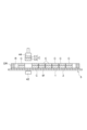
- FIG. 1 is a cross-sectional view that shows a schematic state in which preparations are complete for carrying out the cleaning method according to the present disclosure.
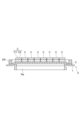
- FIG. 2 is a cross-sectional view showing a schematic diagram of a state in which a semiconductor chip is picked up after cleaning.
- 3A to 3C are cross-sectional views that diagrammatically show the process of manufacturing a semiconductor device by the method according to the first embodiment.
- 4A to 4C are cross-sectional views that diagrammatically show the process of manufacturing a semiconductor device by the method according to the first embodiment.
- FIG. 5 is a cross-sectional view showing a schematic diagram of a state in which the space between two adjacent semiconductor chips is widened by applying tension to an adhesive film.
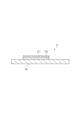
- FIG. 6 is a cross-sectional view showing a schematic state in which one semiconductor chip is bonded onto a substrate.
- FIG. 7 is a cross-sectional view that shows a schematic state in which a plurality of semiconductor chips are stacked on a substrate.
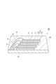
- FIG. 8 is a cross-sectional view showing a schematic example of a semiconductor device having a configuration in which a plurality of semiconductor chips are stacked.
- 9A and 9B are cross-sectional views illustrating the process of manufacturing a semiconductor device by the method according to the second embodiment.
- 10A and 10B are cross-sectional views illustrating the process of manufacturing a semiconductor device by the method according to the second embodiment.
- 11A and 11B are cross-sectional views illustrating the process of manufacturing a semiconductor device by the method according to the third embodiment.
- 12A and 12B are cross-sectional views illustrating the process of manufacturing a semiconductor device by the method according to the third embodiment.
- 13A and 13B are cross-sectional views illustrating the process of manufacturing a semiconductor device by the method according to the fourth embodiment.
- 14A to 14C are cross-sectional views showing a schematic process for manufacturing a semiconductor device by the method according to the fifth embodiment.
- Figure 1 is a cross-sectional view that shows a state in which preparations are complete for carrying out the cleaning method according to this embodiment.
- a plurality of semiconductor chips C shown in Figure 1 are to be cleaned.
- Figure 2 is a cross-sectional view that shows a state in which the semiconductor chips C are picked up after cleaning.
- the semiconductor chips C are obtained through a process of singulating the workpiece Pw shown in Figure 3(a), and include a circuit layer C1 and a die C2.
- the circuit layer C1 is obtained by singulating the circuit layer Lc
- the die C2 is obtained by singulating the semiconductor wafer W (see Figure 4(c)).
- the cleaning method includes the following steps. (a) A step of cleaning, with a chemical solution, a plurality of semiconductor chips C arranged in a region R on the surface 5f of the adhesive film 5 and in a dicing ring DR attached to the surface 5f. (b) A step of picking up the semiconductor chip C from above the surface after cleaning.
- multiple semiconductor chips C are arranged in a region R surrounded by a dicing ring DR.
- the semiconductor chips C are cleaned by spraying a chemical solution from a nozzle toward the semiconductor chips C.
- the chemical solution is, for example, a solvent-based chemical solution, an acid-based chemical solution, or an alkaline-based chemical solution.
- the solvent-based chemical solution contains, for example, NMP (N-methyl-2-pyrrolidone), MEK (methyl ethyl ketone), PGMEA (propylene glycol monomethyl ether acetate), DMSO (dimethyl sulfoxide) or cyclopentanone, and can effectively remove foreign matter such as cutting debris, grinding debris, processing debris, and dust from the semiconductor chip C.
- NMP N-methyl-2-pyrrolidone
- MEK methyl ethyl ketone
- PGMEA propylene glycol monomethyl ether acetate
- DMSO dimethyl sulfoxide
- cyclopentanone cyclopentanone
- the acid-based chemical solution contains, for example, sulfuric acid, citric acid, or hydrofluoric acid, and can effectively remove foreign matter such as cutting debris, grinding debris, processing debris, and dust from the semiconductor chip C.
- the alkaline chemical solution contains, for example, potassium hydroxide, sodium hydroxide, ammonium hydroxide, sodium bicarbonate, hydroxylamine, TMAH (tetramethylammonium hydroxide) or aqueous ammonia, and can effectively remove foreign matter such as cutting chips, grinding chips, processing chips and dust from the semiconductor chip C.
- the adhesive film 5 is composed of a base film 1 and an adhesive layer 2 formed on the surface of the base film 1.
- the base film 1 include plastic films such as polytetrafluoroethylene film, polyethylene terephthalate film, polyethylene film, polypropylene film, polymethylpentene film, and polyimide film. Of these, a film that is resistant to the chemicals used to clean the semiconductor chips C may be used. If necessary, a surface treatment such as primer application, UV treatment, corona discharge treatment, polishing treatment, or etching treatment may be performed.
- the adhesive layer 2 is formed, for example, through a process of applying a coating liquid containing a resin composition having a suitable adhesive strength to the surface of the substrate film 1.
- a resin composition that is resistant to the chemicals used to clean the semiconductor chips C may be used.
- the adhesive layer 2 may have the property that its adhesive strength decreases when exposed to activation energy (e.g., ultraviolet light).
- the semiconductor chip C is pushed up by a push-up jig 42 to peel the semiconductor chip C from the adhesive layer 2, and the semiconductor chip C is picked up by suction with a suction collet 44.
- the adhesive layer 2 is one whose adhesive strength decreases when exposed to activation energy, the adhesive layer 2 is irradiated with activation energy rays prior to picking up.
- the amount of irradiation is, for example, 10 to 1000 mJ/ cm2 , and may be 100 to 700 mJ/ cm2 or 200 to 500 mJ/ cm2 .
- the cleaning method of this embodiment by cleaning the semiconductor chip C on the adhesive film 5 with a chemical solution, foreign matter adhering to the semiconductor chip C can be removed to a greater extent than by cleaning with water.
- a semiconductor device with excellent connection reliability can be manufactured.
- This cleaning method is also useful in that it can be efficiently carried out in the semiconductor manufacturing process. That is, according to this cleaning method, the advanced cleaning with a chemical solution is carried out on the surface 5f of the adhesive film 5 and with the dicing ring DR attached to the adhesive film 5, so that the semiconductor chip C after cleaning can be picked up and directly subjected to the next process.
- the semiconductor chip C may be cleaned with pure water before and/or after cleaning with the chemicals.
- the method for manufacturing a semiconductor device includes the following steps.
- (3a) A step of cutting the circuit layer Lc through the grooves G1 by plasma dicing and half-cutting the semiconductor wafer W to form grooves G2 (see FIG. 3(c)).
- (4a) A step of stripping the photoresist Rp from the circuit layer Lc (see FIG. 4(a)).
- (5a) A step of adhering a backgrind tape TBG so as to cover the circuit layer Lc (see FIG. 4(b)).
- (6a) A step of obtaining a plurality of semiconductor chips C on the surface of the backgrind tape T BG by grinding the semiconductor wafer W from the second surface f2 side (see FIG. 4(c)).
- the workpiece Pw shown in FIG. 3(a) includes a semiconductor wafer W and a circuit layer Lc.
- the thickness of the semiconductor wafer W is, for example, 5 to 775 ⁇ m, and may be 50 to 300 ⁇ m.
- the diameter of the semiconductor wafer W is, for example, 50 to 300 mm, and may be 150 to 300 mm.
- the circuit layer Lc has various electronic circuits (e.g., integrated circuits and power supply circuits) formed thereon depending on the application of the semiconductor device.
- the thickness of the circuit layer Lc is, for example, 0.01 to 50 ⁇ m, and may be 0.1 to 10 ⁇ m.
- the photoresist Rp is made of a photosensitive insulating material, and a groove portion G1 can be formed in the photoresist Rp by a photolithography process (FIG. 3(b)).
- the groove G2 shown in FIG. 3(c) penetrates the circuit layer Lc and extends from the first surface f1 to the inside of the semiconductor wafer W.
- the groove G2 does not reach the second surface f2.
- the groove G2 is formed by plasma dicing.
- a process called the Bosch process a process called the Bosch process is known.
- a passivation step using C 4 F 8 plasma and an etching step using SF 6 plasma are alternately performed to etch the silicon constituting the semiconductor wafer W. That is, in the passivation step, a fluorocarbon-based polymer film (hereinafter simply referred to as the "polymer film”) is isotropically formed on the entire inner surface of the groove G1.
- the etching step a bias is applied to the semiconductor wafer W, and the polymer film at the bottom of the groove G1 is removed by etching with ions.
- the polymer film on the sidewall of the groove G1 is not removed and forms the sidewall of the groove G1.
- Only the silicon exposed at the bottom of the groove G1 from which the polymer film has been removed is etched by fluorine radicals.
- the groove G2 is formed.
- the side surface of the groove G2 thus formed is covered with a polymer film. If the polymer film peels off in a subsequent process, it may become a foreign object that reduces the reliability of the semiconductor device.
- the circuit layer Lc is divided by the groove G2, thereby forming a plurality of circuit layers C1.
- the thickness of the die C2 (the thickness of the semiconductor chip C excluding the circuit layer C1) is, for example, 5 to 775 ⁇ m, and may be 50 to 300 ⁇ m. Grinding debris generated in the above step (6a) can also become foreign matter that reduces the reliability of the semiconductor device.
- tension may be applied to the adhesive film 5 to widen the gap between two adjacent semiconductor chips C. That is, as shown in FIG. 5, tension is applied to the adhesive film 5 by pushing up the inside of the dicing ring DR with the ring Ra from the base film 1 side of the adhesive film 5.
- This makes it easier to supply the chemical solution to the side of the semiconductor chip C in the above step (8a), and the polymer film adhering to the side can be sufficiently removed with the chemical solution.
- HFE hydrofluoroether
- HAD hydroxylamine
- FIG. 6 is a cross-sectional view showing a schematic state in which a semiconductor chip C is bonded to a substrate 10 (adherend) after cleaning.
- a die bonding film (not shown) is used to bond the semiconductor chip C to the substrate 10.
- the object (adherend) to which the second and subsequent semiconductor chips C are bonded is the semiconductor chip C in the lower layer.
- the method for manufacturing a semiconductor device includes the following steps. (1b) A step of placing a workpiece Pw in a region R within a dicing ring DR attached onto the surface 5f of an adhesive film 5 (see FIG. 9(a)). (2b) A step of forming a photoresist Rp so as to cover the circuit layer Lc (see FIG. 9(b)). (3b) A process of forming a groove portion G3 in the photoresist Rp, which reaches the circuit layer Lc, by performing exposure and development processing on the photoresist Rp (see FIG. 10(a)).
- (4b) A process of cutting the circuit layer Lc and the semiconductor wafer W through the grooves G3 by plasma dicing to obtain a plurality of semiconductor chips C on the front surface 5f of the adhesive film 5 (see FIG. 10(b)).
- (5b) A step of carrying out the above-mentioned semiconductor chip cleaning method (see FIGS. 1 and 2).
- (6b) A step of bonding the cleaned semiconductor chip C to an adherend (see FIG. 6).
- the present embodiment will be described mainly with respect to the differences from the first embodiment.
- the above steps (2b) to (5b) are performed on the surface of the adhesive film 5 to which the dicing ring DR is attached.
- the photoresist Rp remains on the upper surface of the semiconductor chip C.
- the photoresist Rp may be removed using a resist remover prior to performing the above step (5b), or may be removed using a chemical solution in the above step (5b). It is preferable to use a solvent-based chemical solution (especially NMP) to remove the photoresist Rp.
- NMP solvent-based chemical solution
- the groove portion G4 may be formed by plasma dicing, as with the above groove portion G2.
- the polymer film resulting from plasma dicing may be removed using an HFE-based or HDA-based chemical solution, as with the first embodiment.
- the method for manufacturing a semiconductor device includes the following steps. (1c) A step of placing a workpiece Pw in region R within a dicing ring DR attached onto surface 5f of adhesive film 5 (see FIG. 11(a)). (2c) A step of forming a protective film Mp so as to cover the circuit layer Lc (see FIG. 11(b)). (3c) A step of cutting the protective film Mp and the circuit layer Lc with a laser to form a groove portion G5 reaching the first surface f1 of the semiconductor wafer W (see FIG. 12(a)).
- (4c) A process of cutting the semiconductor wafer W through the grooves G5 by plasma dicing to obtain a plurality of semiconductor chips C on the front surface 5f of the adhesive film 5 (see FIG. 12(b)).
- (5c) A step of carrying out the above-mentioned semiconductor chip cleaning method (see FIGS. 1 and 2).
- (6c) A step of bonding the washed semiconductor chip C to an adherend (see FIG. 6).
- a protective film Mp is formed in the above step (2c).
- the protective film Mp is intended to prevent the circuit layer Lc from being damaged.
- the protective film Mp is made of, for example, a water-soluble resin, and can be formed by applying a coating containing such a resin to the surface of the workpiece Pw.
- the protective film Mp remains on the upper surface of the semiconductor chip C after the above step (4c) (see FIG. 12(b)).
- the protective film Mp is removed by pure water in the above step (5c).
- the groove portion G6 shown in FIG. 12(b) penetrates the semiconductor wafer W and reaches the surface 5f of the adhesive film 5.
- the groove portion G6 may be formed by plasma dicing, as with the above groove portion G2.
- the polymer film resulting from plasma dicing may be removed using an HFE-based or HDA-based chemical solution, as with the first embodiment.
- the grooves G6 may be formed by blade dicing instead of plasma dicing.
- the circuit layer Lc includes a low-k film
- the circuit layer Lc is cut by a laser to form the grooves G5 in order to prevent the peeling of the low-k film, which has a relatively low mechanical strength.
- the process of cutting the semiconductor wafer W (the process of forming the grooves G6) may be performed by blade dicing.
- the low-k film is a film made of a material with a low dielectric constant, and is mainly used as an interconnect layer, that is, an insulating material between metal wiring that electrically connects different electronic components in a chip.
- the use of the low-k film can reduce the parasitic capacitance between wiring, thereby improving the signal transmission speed and suppressing crosstalk between wiring.
- the process of forming grooves in the circuit layer Lc by a laser is called laser grooving.
- the method for manufacturing a semiconductor device includes the following steps. (1d) A step of placing a workpiece Pw in region R within a dicing ring DR attached to surface 5f of adhesive film 5 (see FIG. 13(a)). (2d) A process of cutting the workpiece Pw by blade dicing to obtain a plurality of semiconductor chips C on the front surface 5f of the adhesive film 5 (see FIG. 13(b)). (3d) A step of carrying out the above-mentioned semiconductor chip cleaning method (see FIGS. 1 and 2). (4d) A step of bonding the cleaned semiconductor chip to an adherend (see FIG. 6).
- the workpiece Pw is divided into a plurality of semiconductor chips C by blade dicing.
- the grooves G7 formed by blade dicing penetrate the circuit layer Lc and the semiconductor wafer W, and reach the surface 5f of the adhesive film 5.
- the grinding debris generated in the above step (2d) can become foreign matter that reduces the reliability of the semiconductor device.
- the above-mentioned solvent-based, acid-based or alkaline-based chemicals are preferably used as the chemical for removing the grinding debris generated by blade dicing. According to this embodiment, the process of forming a photoresist or a protective film is not necessary, and the process of removing them is also not necessary.
- the method for manufacturing a semiconductor device includes the following steps. (1e) A step of placing a workpiece Pw in region R within a dicing ring DR attached onto surface 5f of adhesive film 5 (see FIG. 14(a)). (2e) A step of cutting the circuit layer Lc with a laser to form a groove portion G8 reaching the first surface f1 of the semiconductor wafer W (see FIG. 14(b)). (3e) A process of cutting the semiconductor wafer W through the grooves G8 by blade dicing to obtain a plurality of semiconductor chips C on the front surface 5f of the adhesive film 5 (see FIG. 14(c)). (4e) A step of carrying out the above-mentioned semiconductor chip cleaning method (see FIGS. 1 and 2). (5e) A step of bonding the cleaned semiconductor chip to an adherend (see FIG. 6).
- the circuit layer Lc is cut by a laser. Since a laser is used to cut the circuit layer Lc, even if the circuit layer Lc includes a low-k film, peeling of the low-k film can be suppressed.
- the semiconductor wafer W is cut by blade dicing.
- the groove portion G9 shown in FIG. 14(c) penetrates the semiconductor wafer W and reaches the surface 5f of the adhesive film 5.
- the grinding debris generated in the above steps (2e) and (3e) can become foreign matter that reduces the reliability of the semiconductor device. According to this embodiment, the grinding debris generated in these steps can be removed in the subsequent step (4e).
- the chemical solution it is preferable to use the above solvent-based, acid-based, or alkaline-based chemical solution.
- the semiconductor wafer W is used as is without backgrinding, but the semiconductor wafer W may be backgrinded before being placed in the region R of the adhesive film 5. That is, in the above-mentioned specific embodiment, before placing the workpiece Pw in the region R of the adhesive film 5, the semiconductor wafer W may be ground from the second surface f2 side with a backgrind tape attached to the workpiece Pw so as to cover the circuit layer Lc.
- the circuit layer Lc may also include a low-k film.
Landscapes
- Cleaning Or Drying Semiconductors (AREA)
- Dicing (AREA)
Priority Applications (5)
| Application Number | Priority Date | Filing Date | Title |
|---|---|---|---|
| CN202480027940.1A CN121002620A (zh) | 2023-05-01 | 2024-04-25 | 半导体芯片的清洗方法及半导体装置的制造方法 |
| JP2025518141A JP7794362B2 (ja) | 2023-05-01 | 2024-04-25 | 半導体チップの洗浄方法及び半導体装置の製造方法 |
| KR1020257034723A KR20260002717A (ko) | 2023-05-01 | 2024-04-25 | 반도체 칩의 세정 방법 및 반도체 장치의 제조 방법 |
| JP2025188267A JP7819808B2 (ja) | 2023-05-01 | 2025-11-07 | 半導体チップの洗浄方法及び半導体装置の製造方法 |
| JP2026020196A JP2026066333A (ja) | 2023-05-01 | 2026-02-10 | 半導体チップの洗浄方法 |
Applications Claiming Priority (2)
| Application Number | Priority Date | Filing Date | Title |
|---|---|---|---|
| JP2023-075732 | 2023-05-01 | ||
| JP2023075732 | 2023-05-01 |
Publications (1)
| Publication Number | Publication Date |
|---|---|
| WO2024228364A1 true WO2024228364A1 (ja) | 2024-11-07 |
Family
ID=93333002
Family Applications (1)
| Application Number | Title | Priority Date | Filing Date |
|---|---|---|---|
| PCT/JP2024/016316 Ceased WO2024228364A1 (ja) | 2023-05-01 | 2024-04-25 | 半導体チップの洗浄方法及び半導体装置の製造方法 |
Country Status (5)
| Country | Link |
|---|---|
| JP (3) | JP7794362B2 (https=) |
| KR (1) | KR20260002717A (https=) |
| CN (1) | CN121002620A (https=) |
| TW (1) | TW202445727A (https=) |
| WO (1) | WO2024228364A1 (https=) |
Citations (10)
| Publication number | Priority date | Publication date | Assignee | Title |
|---|---|---|---|---|
| JP2010093273A (ja) * | 2009-11-13 | 2010-04-22 | Casio Computer Co Ltd | 半導体装置の製造方法 |
| JP2012169484A (ja) * | 2011-02-15 | 2012-09-06 | Nitto Denko Corp | 半導体装置の製造方法 |
| JP2016034993A (ja) * | 2014-08-01 | 2016-03-17 | リンテック株式会社 | 粘着シート |
| JP2016039186A (ja) * | 2014-08-05 | 2016-03-22 | 株式会社ディスコ | ウエーハの加工方法 |
| JP2018190902A (ja) * | 2017-05-10 | 2018-11-29 | 株式会社ディスコ | 加工方法 |
| JP2018195746A (ja) * | 2017-05-19 | 2018-12-06 | 日東電工株式会社 | ダイシングダイボンドフィルム |
| JP2018200957A (ja) * | 2017-05-26 | 2018-12-20 | パナソニックIpマネジメント株式会社 | 素子チップの製造方法 |
| JP2020188154A (ja) * | 2019-05-15 | 2020-11-19 | パナソニックIpマネジメント株式会社 | 樹脂組成物、樹脂被覆基板および素子チップの製造方法 |
| WO2022250130A1 (ja) * | 2021-05-28 | 2022-12-01 | 三井化学東セロ株式会社 | バックグラインド用粘着性フィルムおよび電子装置の製造方法 |
| JP2023043724A (ja) * | 2021-09-16 | 2023-03-29 | 古河電気工業株式会社 | 半導体加工用テープ、及び半導体チップの製造方法 |
Family Cites Families (3)
| Publication number | Priority date | Publication date | Assignee | Title |
|---|---|---|---|---|
| JP2001197431A (ja) | 2000-11-02 | 2001-07-19 | Sony Corp | 情報処理装置および情報処理方法、並びにプログラム格納媒体 |
| CN111739854B (zh) | 2020-07-06 | 2022-03-29 | 绍兴同芯成集成电路有限公司 | 一种开窗孔双面电镀厚铜膜 |
| JP2022096079A (ja) | 2020-12-17 | 2022-06-29 | パナソニックIpマネジメント株式会社 | 素子チップの製造方法 |
-
2024
- 2024-04-25 WO PCT/JP2024/016316 patent/WO2024228364A1/ja not_active Ceased
- 2024-04-25 KR KR1020257034723A patent/KR20260002717A/ko active Pending
- 2024-04-25 JP JP2025518141A patent/JP7794362B2/ja active Active
- 2024-04-25 CN CN202480027940.1A patent/CN121002620A/zh active Pending
- 2024-04-26 TW TW113115719A patent/TW202445727A/zh unknown
-
2025
- 2025-11-07 JP JP2025188267A patent/JP7819808B2/ja active Active
-
2026
- 2026-02-10 JP JP2026020196A patent/JP2026066333A/ja active Pending
Patent Citations (10)
| Publication number | Priority date | Publication date | Assignee | Title |
|---|---|---|---|---|
| JP2010093273A (ja) * | 2009-11-13 | 2010-04-22 | Casio Computer Co Ltd | 半導体装置の製造方法 |
| JP2012169484A (ja) * | 2011-02-15 | 2012-09-06 | Nitto Denko Corp | 半導体装置の製造方法 |
| JP2016034993A (ja) * | 2014-08-01 | 2016-03-17 | リンテック株式会社 | 粘着シート |
| JP2016039186A (ja) * | 2014-08-05 | 2016-03-22 | 株式会社ディスコ | ウエーハの加工方法 |
| JP2018190902A (ja) * | 2017-05-10 | 2018-11-29 | 株式会社ディスコ | 加工方法 |
| JP2018195746A (ja) * | 2017-05-19 | 2018-12-06 | 日東電工株式会社 | ダイシングダイボンドフィルム |
| JP2018200957A (ja) * | 2017-05-26 | 2018-12-20 | パナソニックIpマネジメント株式会社 | 素子チップの製造方法 |
| JP2020188154A (ja) * | 2019-05-15 | 2020-11-19 | パナソニックIpマネジメント株式会社 | 樹脂組成物、樹脂被覆基板および素子チップの製造方法 |
| WO2022250130A1 (ja) * | 2021-05-28 | 2022-12-01 | 三井化学東セロ株式会社 | バックグラインド用粘着性フィルムおよび電子装置の製造方法 |
| JP2023043724A (ja) * | 2021-09-16 | 2023-03-29 | 古河電気工業株式会社 | 半導体加工用テープ、及び半導体チップの製造方法 |
Also Published As
| Publication number | Publication date |
|---|---|
| JP2026066333A (ja) | 2026-04-16 |
| JP7819808B2 (ja) | 2026-02-25 |
| JP2026009401A (ja) | 2026-01-19 |
| KR20260002717A (ko) | 2026-01-06 |
| CN121002620A (zh) | 2025-11-21 |
| JPWO2024228364A1 (https=) | 2024-11-07 |
| JP7794362B2 (ja) | 2026-01-06 |
| TW202445727A (zh) | 2024-11-16 |
Similar Documents
| Publication | Publication Date | Title |
|---|---|---|
| TWI855065B (zh) | 封裝結構及製作方法 | |
| JP7129427B2 (ja) | 処理された積層ダイ | |
| KR100741864B1 (ko) | 반도체장치의 제조방법 | |
| US8883615B1 (en) | Approaches for cleaning a wafer during hybrid laser scribing and plasma etching wafer dicing processes | |
| TWI698954B (zh) | 切割晶圓背側上具有焊料凸塊的晶圓 | |
| JP6519759B2 (ja) | 素子チップの製造方法 | |
| JP6524594B2 (ja) | 素子チップの製造方法 | |
| JP7233019B2 (ja) | 素子チップの製造方法 | |
| US10410923B2 (en) | Method of processing wafer | |
| US9105710B2 (en) | Wafer dicing method for improving die packaging quality | |
| CN113649709A (zh) | 晶圆切割方法 | |
| JP7819808B2 (ja) | 半導体チップの洗浄方法及び半導体装置の製造方法 | |
| CN114628250A (zh) | 晶圆划片方法 | |
| JP6062254B2 (ja) | ウエーハの加工方法 | |
| US20240006239A1 (en) | Device wafer processing method | |
| JP2019169686A (ja) | 素子チップの製造方法 | |
| JPWO2024228364A5 (https=) | ||
| JPH0778868A (ja) | 誘電体分離基板の製造方法 |
Legal Events
| Date | Code | Title | Description |
|---|---|---|---|
| 121 | Ep: the epo has been informed by wipo that ep was designated in this application |
Ref document number: 24800095 Country of ref document: EP Kind code of ref document: A1 |
|
| ENP | Entry into the national phase |
Ref document number: 2025518141 Country of ref document: JP Kind code of ref document: A |
|
| WWE | Wipo information: entry into national phase |
Ref document number: 2025518141 Country of ref document: JP |
|
| NENP | Non-entry into the national phase |
Ref country code: DE |