WO2024225312A1 - ゲートドライブ回路 - Google Patents
ゲートドライブ回路 Download PDFInfo
- Publication number
- WO2024225312A1 WO2024225312A1 PCT/JP2024/016058 JP2024016058W WO2024225312A1 WO 2024225312 A1 WO2024225312 A1 WO 2024225312A1 JP 2024016058 W JP2024016058 W JP 2024016058W WO 2024225312 A1 WO2024225312 A1 WO 2024225312A1
- Authority
- WO
- WIPO (PCT)
- Prior art keywords
- signal
- gate drive
- pair
- circuit
- input
- Prior art date
- Legal status (The legal status is an assumption and is not a legal conclusion. Google has not performed a legal analysis and makes no representation as to the accuracy of the status listed.)
- Ceased
Links
Images



Classifications
-
- H—ELECTRICITY
- H04—ELECTRIC COMMUNICATION TECHNIQUE
- H04L—TRANSMISSION OF DIGITAL INFORMATION, e.g. TELEGRAPHIC COMMUNICATION
- H04L25/00—Baseband systems
- H04L25/02—Details ; arrangements for supplying electrical power along data transmission lines
- H04L25/0264—Arrangements for coupling to transmission lines
- H04L25/0272—Arrangements for coupling to multiple lines, e.g. for differential transmission
-
- H—ELECTRICITY
- H03—ELECTRONIC CIRCUITRY
- H03F—AMPLIFIERS
- H03F3/00—Amplifiers with only discharge tubes or only semiconductor devices as amplifying elements
- H03F3/20—Power amplifiers, e.g. Class B amplifiers, Class C amplifiers
- H03F3/21—Power amplifiers, e.g. Class B amplifiers, Class C amplifiers with semiconductor devices only
- H03F3/217—Class D power amplifiers; Switching amplifiers
- H03F3/2173—Class D power amplifiers; Switching amplifiers of the bridge type
-
- H—ELECTRICITY
- H03—ELECTRONIC CIRCUITRY
- H03F—AMPLIFIERS
- H03F3/00—Amplifiers with only discharge tubes or only semiconductor devices as amplifying elements
- H03F3/30—Single-ended push-pull [SEPP] amplifiers; Phase-splitters therefor
- H03F3/3001—Single-ended push-pull [SEPP] amplifiers; Phase-splitters therefor with field-effect transistors
-
- H—ELECTRICITY
- H03—ELECTRONIC CIRCUITRY
- H03F—AMPLIFIERS
- H03F3/00—Amplifiers with only discharge tubes or only semiconductor devices as amplifying elements
- H03F3/45—Differential amplifiers
- H03F3/45071—Differential amplifiers with semiconductor devices only
- H03F3/45076—Differential amplifiers with semiconductor devices only characterised by the way of implementation of the active amplifying circuit in the differential amplifier
- H03F3/4508—Differential amplifiers with semiconductor devices only characterised by the way of implementation of the active amplifying circuit in the differential amplifier using bipolar transistors as the active amplifying circuit
- H03F3/45085—Long tailed pairs
- H03F3/45094—Folded cascode stages
-
- H—ELECTRICITY
- H03—ELECTRONIC CIRCUITRY
- H03K—PULSE TECHNIQUE
- H03K17/00—Electronic switching or gating, i.e. not by contact-making and –breaking
- H03K17/51—Electronic switching or gating, i.e. not by contact-making and –breaking characterised by the components used
- H03K17/56—Electronic switching or gating, i.e. not by contact-making and –breaking characterised by the components used by the use, as active elements, of semiconductor devices
- H03K17/687—Electronic switching or gating, i.e. not by contact-making and –breaking characterised by the components used by the use, as active elements, of semiconductor devices the devices being field-effect transistors
- H03K17/689—Electronic switching or gating, i.e. not by contact-making and –breaking characterised by the components used by the use, as active elements, of semiconductor devices the devices being field-effect transistors with galvanic isolation between the control circuit and the output circuit
- H03K17/691—Electronic switching or gating, i.e. not by contact-making and –breaking characterised by the components used by the use, as active elements, of semiconductor devices the devices being field-effect transistors with galvanic isolation between the control circuit and the output circuit using transformer coupling
-
- H—ELECTRICITY
- H03—ELECTRONIC CIRCUITRY
- H03K—PULSE TECHNIQUE
- H03K19/00—Logic circuits, i.e. having at least two inputs acting on one output; Inverting circuits
- H03K19/0175—Coupling arrangements; Interface arrangements
Definitions
- the present invention relates to a gate drive circuit.
- a primary gate drive signal is input to the primary winding of the pulse transformer, and the output of the secondary winding of the pulse transformer is compared.
- the differential is amplified by the secondary winding and output as a secondary gate drive signal.
- an electrostatic shield grounded to a second ground potential point is provided between the primary winding and the secondary winding of the pulse transformer. The plate is placed.
- the gate drive circuit of Patent Document 1 can remove common mode noise superimposed on the output side, but cannot remove common mode noise superimposed on the input side.
- the present invention has been made to solve these problems, and aims to provide a gate drive circuit that can remove common mode noise superimposed on the output side and input side.
- a gate drive circuit includes a signal conversion circuit that operates with the potential of a first ground as a reference potential and converts a gate control signal, which is a single-ended signal, into a differential signal consisting of a positive signal and a negative signal whose signal level difference corresponds to the gate control signal; a first pulse transformer having a primary winding and a secondary winding that are electrically insulated from each other and each having a neutral point, the neutral point of the primary winding being set to the potential of the first ground and the positive signal and the negative signal of the differential signal being input to both ends of the primary winding, respectively; and a pair of resistance elements connected in series with each other, the ends and connections of the pair of resistance elements being connected to each other.
- the input differential voltage generation circuit has two resistance elements, each of which is electrically connected to both ends of the secondary winding of the first pulse transformer and the neutral point, either directly or via a transmission cable and a second pulse transformer, and generates a pair of input differential voltages based on the potential of the connection points across the pair of resistance elements; a differential amplifier circuit is electrically connected to the input differential voltage generation circuit and differentially amplifies the pair of input differential voltages to output a pair of output differential voltages; and a gate drive signal generation circuit is electrically connected to the differential amplifier circuit and generates a gate drive signal, which is a single-ended signal based on a predetermined potential, based on the pair of output differential voltages, and outputs the gate drive signal to a switching element that operates based on the potential of a second ground.
- the present invention has the effect of providing a gate drive circuit that can remove common mode noise superimposed on the output side and input side.
- FIG. 1 is a circuit diagram showing the configuration of a push-pull amplifier circuit in which a gate drive circuit according to the present disclosure is used.
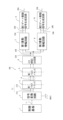
- FIG. 2A is a block diagram showing a first configuration example of the gate drive circuit of FIG.
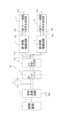
- FIG. 2B is a block diagram showing a second configuration example of the gate drive circuit of FIG.
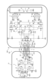
- FIG. 3 is a circuit diagram showing an example of a specific circuit configuration of the first configuration example of the gate drive circuit of FIG. 2A.
- FIG. 4A is a waveform diagram showing the waveform of a differential signal on which common mode noise is superimposed.
- FIG. 4B is a waveform diagram showing the waveform of a differential signal induced in the first pulse transformer by the differential signal of FIG. 4A.
- FIG. 4C is a waveform diagram showing the waveform of an input differential voltage generated by an input differential voltage generating circuit from a signal derived from the differential signal induced in the first pulse transformer of FIG. 4B.
- FIG. 5 is a circuit diagram showing the operation of a switching power supply device using the push-pull amplifier circuit of FIG.
- FIG. 6 is a schematic diagram showing switching noise generated by the switching module of FIG.
- a gate drive circuit includes a signal conversion circuit that operates with the potential of a first ground as a reference potential and converts a gate control signal, which is a single-ended signal, into a differential signal consisting of a positive signal and a negative signal whose signal level difference corresponds to the gate control signal; a first pulse transformer having a primary winding and a secondary winding that are electrically insulated from each other and each having a neutral point, the neutral point of the primary winding being set to the potential of the first ground and the positive signal and the negative signal of the differential signal being input to both ends of the primary winding, respectively; and a pair of resistance elements connected in series with each other, both ends and a connection point of the pair of resistance elements being directly connected to each other.
- the input differential voltage generating circuit is electrically connected to both ends of the secondary winding of the first pulse transformer and the neutral point, respectively, via a transmission cable and a second pulse transformer, and generates a pair of input differential voltages across the pair of resistance elements, with the potential of the connection point as a reference;
- a differential amplifier circuit is electrically connected to the input differential voltage generating circuit and differentially amplifies the pair of input differential voltages to output a pair of output differential voltages;
- a gate drive signal generating circuit is electrically connected to the differential amplifier circuit and generates a gate drive signal, which is a single-ended signal with a predetermined potential as a reference, based on the pair of output differential voltages, and outputs the gate drive signal to a switching element that operates with the potential of a second ground as a reference.
- the input side and output side of the gate drive circuit are insulated from each other by the first pulse transformer, and the input side is based on the potential of the first ground, while the output side is connected to the switching element and is in a floating state based on the potential of the second ground.
- the gate control signal which is a single-ended signal, is converted by the signal conversion circuit into a differential signal consisting of a positive signal and a negative signal whose signal level difference corresponds to the gate control signal, and the neutral point of the primary winding of the first pulse transformer is set to the potential of the first ground, and the differential signal is input to both ends of the primary winding.
- the positive signal and the negative signal are converted into a pair of single-ended voltage signals that are induced in the winding of the same transformer as voltages at both ends, have twice the amplitude, and are in opposite phases (positive and negative). Therefore, when common mode noise is superimposed on these positive and negative signals on the input side, the common mode noise of the positive signal and the common mode noise of the negative signal are inversely positive and negative (plus and minus) to each other, so they are offset and removed in the first pulse transformer.
- both ends and the connection point of the pair of resistive elements of the input differential voltage generating circuit are connected electrically directly or via a transmission cable and a second pulse transformer to both ends and the neutral point of the secondary winding of the first pulse transformer, respectively, and a pair of input differential voltages based on the potential of the connection points are generated across the pair of resistive elements, and this pair of input differential voltages is differentially amplified by the differential amplifier circuit.
- the common mode noise of the pair of wirings has opposite positive and negative values in the pair of input differential voltages generated by the input differential voltage generating circuit, and is removed by the differential amplifier circuit. Also, since the load current of the first pulse transformer flows through the pair of resistive elements of the input differential voltage generating circuit, the impedance of the transmission path of the differential signal is lowered, and the ability to remove common mode noise is improved.
- the second pulse transformer may have a primary winding and a secondary winding that are electrically insulated from each other and each have a neutral point, and both ends and the neutral point of the primary winding are electrically connected to both ends and the neutral point of the secondary winding of the first pulse transformer, respectively, via the transmission cable, and the input differential voltage generating circuit may have both ends and the connection point of the pair of resistive elements connected to both ends and the neutral point of the secondary winding of the second pulse transformer, respectively.
- the common mode noise when common mode noise is superimposed on the secondary winding of the first pulse transformer and the transmission cable, the common mode noise can be removed by the second pulse transformer, just as with the first pulse transformer.
- the control device that generates the gate control signal can be placed away from the switching elements, and the computer that constitutes the control device can be suitably protected from noise generated by the switching operation of the switching elements.
- the two switching elements constitute a first switching element and a second switching element that are push-pull connected to each other
- the differential amplifier circuit includes a first differential amplifier circuit and a second differential amplifier circuit
- the gate drive signal generation circuit includes a first and a second gate drive signal generation circuit
- the first differential amplifier circuit is electrically connected to the input difference voltage generation circuit, and is a circuit that differentially amplifies the pair of input difference voltages to output a pair of first output difference voltages at a high potential
- the second differential amplifier circuit is electrically connected to the input difference voltage generation circuit, and is a circuit that differentially amplifies the pair of input difference voltages to output a pair of first output difference voltages at a low potential that is lower than the pair of first output difference voltages.
- the first gate drive signal generation circuit is electrically connected to the first differential amplifier circuit, and generates a first gate drive signal, which is the gate drive signal based on a positive potential based on the pair of first output difference voltages, and outputs the first gate drive signal to the first switching element.
- the second gate drive signal generation circuit is electrically connected to the second differential amplifier circuit, and generates a second gate drive signal, which is the gate drive signal based on a negative potential based on the pair of second output difference voltages, and outputs the second gate drive signal to the second switching element.
- the first switching element and the second switching element which are connected to each other in a push-pull manner, can be driven while removing common mode noise superimposed on the output side and the input side.
- the gate drive signal generation circuit may include a flip-flop that receives the pair of output difference voltages and outputs a single-ended signal based on a predetermined potential, and outputs the single-ended signal as the gate drive signal.
- the flip-flop can generate a gate drive signal that is a single-ended signal based on a predetermined potential.
- the waveform of the pair of output difference voltages of the differential amplifier circuit can be shaped, which further eliminates common-mode noise.
- FIG. 1 is a circuit diagram showing the configuration of a push-pull amplifier circuit 500 in which the gate drive circuit 100 of the present disclosure is used.
- the push-pull amplifier circuit 500 includes a pair of switching elements 60 connected in a push-pull manner and a gate drive circuit 100.
- the pair of switching elements 60 is configured by connecting a high-side first switching element 61, for example, a PMOSFET, and a low-side second switching element 62, for example, an NMOSFET, in series between a positive power supply VDD and a second ground GND2, and an output is taken out from the connection point between them.
- a high-side first switching element 61 for example, a PMOSFET
- a low-side second switching element 62 for example, an NMOSFET
- the input side and the output side of the gate drive circuit 100 are insulated, the input side is connected to a first ground GND1, and the output side is electrically connected to the pair of switching elements 60. Therefore, the output side is in a floating state with respect to the first ground GND1 on the input side.
- the gate drive circuit 100 generates a gate drive signal from a gate control signal 11 input from a control board 1, and drives the pair of switching elements 60 by the gate drive signal. Next, the configuration of the gate drive circuit 100 will be described.
- the gate drive circuit 100 includes first to third configuration examples.
- FIG. 2A is a block diagram showing a first configuration example of the gate drive circuit 100 of FIG.
- the first configuration example is a configuration example of a gate drive circuit 100 including a transmission cable 4 and a second pulse transformer.
- the gate drive circuit 100 includes a signal conversion circuit 2, a first pulse transformer 3, a transmission cable 4, a second pulse transformer 5, an input difference voltage generation circuit 6, a first differential amplifier circuit 7, a second differential amplifier circuit 8, a first gate drive signal generation circuit 9, and a second gate drive signal generation circuit 10.
- the signal conversion circuit 2 operates with the potential of the first ground GND1 as a reference potential, and converts the gate control signal 11, which is a single-ended signal from the control board 1, into a differential signal 21 consisting of a positive signal 21A and a negative signal 21B whose signal level difference corresponds to the gate control signal 11.
- the first pulse transformer 3 transmits this differential signal 21 to the input differential voltage generating circuit 6 via the transmission cable 4 and the second pulse transformer 5.
- the input side and output side of the gate drive circuit 100 are insulated by the first pulse transformer 3 and the second pulse transformer 5.
- the input differential voltage generating circuit 6 generates a pair of input differential voltages 22A, 22B based on the transmitted differential signal 21.
- the first differential amplifier circuit 7 differentially amplifies the pair of input differential voltages 22A, 22B to output a pair of high potential first output differential voltages 23A, 23B.
- the first gate drive signal generating circuit 9 generates a first gate drive signal 25A based on the pair of first output differential voltages 23A, 23B and uses a predetermined positive potential as a reference, and outputs the first gate drive signal 25A to the first switching element 61 (see FIG. 1).
- the second differential amplifier circuit 8 differentially amplifies the pair of input differential voltages 22A, 22B to output a pair of second output differential voltages 24A, 24B that are lower in potential than the pair of first output differential voltages 23A, 23B.
- the second gate drive signal generation circuit 10 generates a second gate drive signal 25B based on the pair of second output difference voltages 24A, 24B and references a predetermined negative potential, and outputs the second gate drive signal 25B to the second switching element 62 (see FIG. 1).
- This first configuration example is applied when you want to protect the computer that constitutes the control board (control device) 1 by keeping it as far away as possible from the source of common mode noise.
- FIG. 2B is a block diagram showing a second configuration example of the gate drive circuit 100 of FIG. 1.
- the transmission cable 4 and the second pulse transformer 5 are omitted. Therefore, in the second configuration example, the input side and the output side of the gate drive circuit 100 are insulated by the first pulse transformer 3.
- the input differential voltage generating circuit 6 generates a pair of input differential voltages 22A, 22B based on the differential signal 21 output to the secondary winding of the first pulse transformer 3.
- the rest of the configuration is the same as in the first configuration example, so a description thereof will be omitted.
- Such a second configuration example is applied when it is not necessary to place the control board 1 away from the source of common mode noise.
- the gate drive circuit 100 has only one set of differential amplifier circuit and gate drive signal generation circuit (for example, the first differential amplifier circuit 7 and the first gate drive signal generation circuit 9, or the second differential amplifier circuit 8 and the second gate drive signal generation circuit 10).
- the rest of the configuration is the same as the first or second configuration example, so the description will be omitted.
- This third configuration example is applied when driving a single switching element (for example, the first switching element 61 or the second switching element 62 in FIG. 1).
- FIG. 3 is a circuit diagram showing an example of a specific circuit configuration of the first configuration example of the gate drive circuit 100 of FIG. 2A.
- the circuit shown in FIG. 3 includes the gate drive circuit 100 of FIG. 2A and a pair of push-pull connected switching elements 60 of FIG. 1, and is configured as a push-pull amplifier circuit 500.
- the signal conversion circuit 2 includes a logic circuit 31, a positive signal generation circuit 32, and a negative signal generation circuit 33.
- the logic circuit 31 uses a logic circuit to generate the in-phase signal 12A and the anti-phase signal 12B from the gate control signal 11 from the control board 1.
- the positive signal generating circuit 32 is configured with a pair of push-pull connected transistors Q1, Q2, which are connected to a 5V positive power supply and a first ground GND1 via resistor elements R3, R4, respectively. Note that a diode facing in the opposite direction is connected in parallel to the pair of transistors Q1, Q2.
- Transistors Q1 and Q2 are configured, for example, as a PMOSFET and an NMOSFET, and the in-phase signal 12A from the logic circuit 31 is input to their gates via resistor element R1. As a result, the positive signal generating circuit 32 outputs a positive signal that is an amplified version of the in-phase signal 12A from the connection point between transistors Q1 and Q2.
- the negative signal generating circuit 33 is configured with a pair of push-pull connected transistors Q3, Q4, which are connected to a 5V positive power supply and a first ground GND1 via resistor elements R5, R6, respectively. Diodes facing in the opposite direction are connected in parallel to the pair of transistors Q3, Q4.
- Transistors Q3 and Q4 are configured, for example, as a PMOSFET and an NMOSFET, and the antiphase signal 12B from the logic circuit 31 is input to their gates via resistor element R2.
- the negative signal generating circuit 33 outputs a negative signal 21B, which is an amplified version of the antiphase signal 12B, from the connection point between transistors Q3 and Q4.
- the first pulse transformer 3 has a primary winding and a secondary winding that are electrically insulated from each other and each have a neutral point MP1, MP2.
- the neutral point MP1 of the primary winding is connected to the first ground GND1.
- the first end EP1 of the primary winding is connected to the connection point between the transistor Q1 and the transistor Q2 of the positive signal generating circuit 32, and the positive signal 21A is input to the first end EP1.
- the second end EP2 of the primary winding is connected to the connection point between the transistor Q3 and the transistor Q4 of the negative signal generating circuit 33, and the negative signal 21B is input to the second end EP2.
- the second pulse transformer 5 has a primary winding and a secondary winding that are electrically insulated from each other and have neutral points MP3 and MP4, respectively.
- the first end EP5, the second end EP6, and the neutral point MP3 of the primary winding are connected to the first end EP3, the second end EP4, and the neutral point MP2 of the secondary winding of the first pulse transformer 3, respectively, via the transmission cable 4.
- the input differential voltage generating circuit 6 has a pair of resistor elements R9, R10 connected in series.
- the pair of resistor elements R9, R10 have appropriate resistance values that are equal to each other. It is preferable that the resistance values of the pair of resistor elements R9, R10 are equal to each other from the viewpoint of completely canceling out common mode noise. However, the resistance values of the pair of resistor elements R9, R10 do not have to be equal to each other. Even in this case, common mode noise can be reduced, although imperfectly.
- the high potential side end, the low potential side end, and the connection point N1 of the pair of resistor elements R9, R10 are connected to the first end EP7, the second end EP8, and the neutral point MP4 of the secondary winding of the second pulse transformer 5, respectively. As a result, a pair of input differential voltages 22A, 22B based on the potential of the connection point N1 are generated across the pair of resistor elements R9, R10.
- the first differential amplifier circuit 7 includes a pair of transistors Q5 and Q6 as amplifying elements.
- One of the transistors, Q5, is connected to the positive power supply VCC via the transistor Q7 and the resistor element R19, and is connected to the negative power supply VEE via the common resistor element R21.
- the other transistor Q6 is connected to the positive power supply VCC via the transistor Q8 and the resistor element R20, and is connected to the negative power supply VEE via the common resistor element R21.
- the pair of transistors Q5 and Q6 are, for example, npn-type bipolar transistors.
- the base of the transistor Q5 is connected to the high-potential end of the pair of resistor elements R9 and R10 via the base resistor element R17, and an input differential voltage 22A (high-potential side differential voltage) is input to the base of the transistor Q5.
- the base of the transistor Q6 is connected to the low-potential end of the pair of resistor elements R9 and R10 via the base resistor element R18, and an input differential voltage 22B (low-potential side differential voltage) is input to the base of the transistor Q6.
- the gate drive circuit 100 also includes a circuit that resistively divides the voltage between the positive power supply VCC and the negative power supply VEE.
- this circuit for example, four resistor elements R11 to R14 are connected in series between the positive power supply VCC and the negative power supply VEE, and the resistor elements R11 and R14 have the same resistance value, and the resistor elements R12 and R13 have the same resistance value.
- the connection point N2 between the resistor elements R12 and R13 has an intermediate potential between the positive power supply VCC and the negative power supply VEE, and this connection point N2 is connected to the connection point N1 of the input difference voltage generation circuit 6.
- the potential of the connection point N1 is fixed by the positive power supply VCC and the negative power supply VEE, but this configuration may be omitted.
- transistors Q7 and Q8 are connected to the connection point between resistor elements R11 and R12, and the resistance values of these resistor elements R11 and R12 are appropriately selected so that transistors Q7 and Q8 have a predetermined high resistance value.
- the first differential amplifier circuit 7 differentially amplifies the pair of input difference voltages 22A and 22B and outputs a pair of first output difference voltages 23A and 23B to the connection points N3 and N4, respectively.
- the second differential amplifier circuit 8 includes a pair of transistors Q9 and Q10 as amplifying elements.
- One of the transistors Q9 is connected to the positive power supply VCC via a common resistor element R22 and is connected to the negative power supply VEE via a transistor Q11 and a resistor element R23.
- the other transistor Q10 is connected to the positive power supply VCC via a common resistor element R22 and is connected to the negative power supply VEE via a transistor Q12 and a resistor element R24.
- the pair of transistors Q9 and Q10 are, for example, pnp-type bipolar transistors.
- the base of the transistor Q9 is connected to the high-potential end of the pair of resistor elements R9 and R10 via a base resistor element R16, and an input differential voltage 22A (high-potential side differential voltage) is input to the base of the transistor Q9.
- the base of the transistor Q10 is connected to the low-potential end of the pair of resistor elements R9 and R10 via a base resistor element R15, and an input differential voltage 22B (low-potential side differential voltage) is input to the base of the transistor Q9.
- transistors Q11 and Q12 are connected to the connection point between resistor elements R13 and R14, and the resistance values of these resistor elements R13 and R14 are appropriately selected so that transistors Q11 and Q12 have a predetermined high resistance value.
- the second differential amplifier circuit 8 differentially amplifies the pair of input difference voltages 22A and 22B and outputs a pair of second output difference voltages 24A and 24B to the connection points N5 and N6, respectively.
- the first gate drive signal generating circuit 9 is composed of a square wave waveform shaping circuit.
- an RS flip-flop which is a logic circuit, is used as this waveform shaping circuit.
- This RS flip-flop operates based on a predetermined high potential.
- the set input terminal of this RS flip-flop is connected to the connection point N3 via a resistor element R25
- the reset input terminal is connected to the connection point N4 via a resistor element R26
- the set output terminal is connected to the gate of the first switching element 61.
- a pair of first output difference voltages 23A and 23B consisting of single-ended signals of opposite phases are input to the set input terminal and the reset input terminal, so that a single-ended signal of the same phase as the first output difference voltage 23A is output to the set output terminal.
- the first gate drive signal generating circuit 9 outputs this single-ended signal to the first switching element 61 as the first gate drive signal 25A.
- the second gate drive signal generating circuit 10 is composed of a square wave waveform shaping circuit.
- an RS flip-flop which is a logic circuit, is used as this waveform shaping circuit.
- This RS flip-flop operates based on a predetermined low potential.
- the set input terminal of this RS flip-flop is connected to the connection point N5 via a resistor element R28, the reset input terminal is connected to the connection point N6 via a resistor element R27, and the set output terminal is connected to the gate of the second switching element 62.
- a pair of second output difference voltages 24A and 24B consisting of single-ended signals of opposite phases are input to the set input terminal and the reset input terminal, so that a single-ended signal of the same phase as the second output difference voltage 24A is output to the set output terminal.
- the second gate drive signal generating circuit 10 outputs this single-ended signal to the second switching element 62 as the second gate drive signal 25B.
- Fig. 4A is a waveform diagram showing the waveform of the differential signal 21 on which common mode noise is superimposed.
- the upper waveform diagram of Fig. 4A shows the waveform of the positive signal 21A
- the lower waveform diagram of Fig. 4A shows the waveform of the negative signal 21B.
- Fig. 4B is a waveform diagram showing the waveform of the differential signal 21 induced in the first pulse transformer 3 by the differential signal 21 of Fig. 4A.
- Fig. 4C is a waveform diagram showing the waveforms of the input differential voltages 22A and 22B generated by the input differential voltage generating circuit 6 from the signal derived from the differential signal 21 induced in the first pulse transformer 3 of Fig. 4B.
- the logic circuit 31 generates an in-phase signal 12A and an anti-phase signal 12B from the gate control signal 11 from the control board 1.
- the positive signal generating circuit 32 outputs a positive signal 21A obtained by amplifying the in-phase signal 12A.
- the negative signal generating circuit 33 outputs a negative signal 21B obtained by amplifying the anti-phase signal 12B.
- the positive signal 21A and the negative signal 21B are input to the first end EP1 and the second end EP2 of the primary winding of the first pulse transformer 3, respectively.
- the positive signal 21A and the negative signal 21B are both single-ended signals that take two values, a high level of a positive voltage (5V) and a low level of zero voltage (potential of the first ground GND1 is 0V), and have opposite phases.
- the positive signal 21A and the negative signal 21B are input to the first end EP1 and the second end EP2 of the primary winding, respectively.
- the positive voltage of the positive signal 21A is applied to the first terminal EP1 in the primary winding of the first pulse transformer, and the zero voltage of the negative signal 21B is applied to the second terminal EP2, so that an excitation current flows from the first terminal EP1 to the neutral point MP1.
- this induces a voltage from the second terminal EP2 to the first terminal EP1 in the primary winding of the first pulse transformer 3.
- the potential of the neutral point MP1 of the primary winding is 0V
- the voltage V1 of the first terminal EP1 becomes a positive voltage.
- the second terminal EP2 since the second terminal EP2 is connected to the first ground GND1 via the resistive element R8 at this time t0, the voltage V2 of the second terminal EP2 becomes a negative voltage, and a current flows from the neutral point MP1 to the second terminal EP2. At this time, the excitation current induces a voltage in the secondary winding of the first pulse transformer 3 and the primary winding and secondary winding of the second pulse transformer 5 according to the turns ratio of the first pulse transformer 3 and the second pulse transformer 5.
- the zero voltage of the positive signal 21A is applied to the first terminal EP1 and the positive voltage of the negative signal 21B is applied to the second terminal EP2 in the primary winding of the first pulse transformer 3, so that an excitation current flows from the second terminal EP2 to the neutral point MP1.
- This induces a voltage from the first terminal EP1 to the second terminal EP2 in the primary winding of the first pulse transformer 3.
- the potential of the neutral point MP1 of the primary winding is 0V
- the voltage V2 of the second terminal EP2 becomes a positive voltage.
- the voltage V1 of the first terminal EP1 becomes a negative voltage, and a current flows from the neutral point MP1 to the first terminal EP1.
- the excitation current induces a voltage in the secondary winding of the first pulse transformer 3 and the primary winding and secondary winding of the second pulse transformer 5 according to the turn ratio of the first pulse transformer 3 and the second pulse transformer 5.
- the positive signal 21A and the negative signal 21B are converted by the first pulse transformer 3 into a pair of single-ended voltage signals with voltages V1 and V2, respectively, having twice the amplitude and in opposite phases (positive and negative are reversed), and are transmitted to the secondary winding of the second pulse transformer 5 via the transmission cable 4.
- the common mode noise removal action on the input side of the gate drive circuit 100 will be described.
- FIG. 4A for example, assume that common mode noise is superimposed on the positive signal 21A and the negative signal 21B between time t0 and time t1.
- the common mode noise superimposed on the positive signal 21A causes an excitation current to flow between the first end EP1 and the neutral point MP1 of the primary winding of the first pulse transformer 3
- the common mode noise superimposed on the negative signal 21B causes an excitation current to flow between the second end EP2 and the neutral point MP1 of the primary winding of the first pulse transformer 3.
- FIG. 4A for example, assume that common mode noise is superimposed on the positive signal 21A and the negative signal 21B between time t0 and time t1.
- the common mode noise superimposed on the positive signal 21A causes an excitation current to flow between the first end EP1 and the neutral point MP1 of the primary winding of the first pulse transformer 3
- the common mode noise superimposed on the negative signal 21B causes an excitation current to flow between the second
- the input differential voltages 22A and 22B are generated from a pair of single-ended voltage signals transmitted to the secondary winding of the second pulse transformer 5 as follows.
- a single-ended voltage signal corresponding to the voltage V1 in FIG. 4B appears at the high-potential end of the resistor element R9.
- the connection point N2 is used as a reference, the intermediate voltage of the amplitude of this single-ended voltage signal becomes a low-level zero voltage, so that it becomes a single-ended voltage signal having a waveform as shown in the upper part of FIG. 4C.
- connection point N2 When the connection point N2 is used as a reference, the intermediate voltage of the amplitude of this single-ended voltage signal becomes a low-level zero voltage, so that it becomes a single-ended voltage signal having a waveform as shown in the lower part of FIG. 4C. Therefore, the pair of input differential voltages 22A and 22B have waveforms corresponding to the positive signal 21A and the negative signal 21B in FIG. 4A, respectively.
- FIG. 3 shows the current through the transmission path of the differential signal 21 when the positive signal 21A is at a high level. This reduces the impedance of the first pulse transformer 3 and the second pulse transformer 5, allowing a large current to pass through the transmission path of the differential signal 21 including the first pulse transformer 3, the transmission cable 4, and the second pulse transformer 5, improving the common mode noise removal capability on the input side of the gate drive circuit 100.
- the common mode noise on the pair of wires has opposite positive and negative values in the pair of input differential voltages 22A and 22B generated by the input differential voltage generating circuit 6.
- the first and second differential amplifier circuits 7 and 8 differentially amplify this pair of input differential voltages 22A and 22B, thereby removing the superimposed common mode noise.
- the timing at which the pair of input differential voltages 22A and 22B are input to the first and second differential amplifier circuits 7 and 8 may be slightly different from each other, and when the first and second differential amplifier circuits 7 and 8 operate at high speed, the slight difference in timing may prevent the common mode noise from being completely removed.
- the first and second gate drive signal generating circuits 9 and 10 are configured as waveform shaping circuits, the waveforms of the pair of first output differential voltages 23A and 23B and the pair of second output differential voltages 24A and 24B output from the first and second differential amplifier circuits 7 and 8 are shaped, thereby removing the remaining components of the common mode noise from the pair of first output differential voltages 23A and 23B and the pair of second output differential voltages 24A and 24B.
- the waveform shaping circuit is a flip-flop, the noise in which the common mode noise is converted to normal mode in the previous circuit is preferably removed. In this way, common mode noise is eliminated at the output side of the gate drive circuit 100.
- the signal conversion circuit 2 and the first pulse transformer 3 are mounted on a first board 81, and the second pulse transformer 5, the input differential voltage generation circuit 6, the first differential amplifier circuit 7, the second differential amplifier circuit 8, the first gate drive signal generation circuit 9, the second gate drive signal generation circuit 10, and a pair of switching elements 60 are mounted on a second board 82.
- the secondary winding of the first pulse transformer 3 on the first board 81 and the primary winding of the second pulse transformer 5 on the second board 82 are connected by a transmission cable 4.
- the second board 82 for example, near a switching module 800 (see FIG. 5) driven by a pair of switching elements 60, and extending the transmission cable 4 to place the first board 81 away from the switching module 800 and near the control board 1, the computer constituting the control board 1 can be suitably protected from common mode noise generated by the switching operation of the switching module 800.
- FIG. 5 is a circuit diagram showing the operation of a switching power supply device 1000 using the push-pull amplifier circuit 500 of Fig. 3.
- reference numerals of detailed elements are omitted in order to make the drawing easier to see.
- the switching power supply device 1000 includes a switching module 800 and first and second push-pull amplifier circuits 500A, 500B.
- the switching module 800 includes a high-side switching element SWH and a low-side switching element SWL.
- the high-side switching element SWH and the low-side switching element SWL are configured, for example, with IGBTs.
- a reverse diode is connected in parallel to each of the high-side switching element SWH and the low-side switching element SWL.
- the first push-pull amplifier circuit 500A includes a first gate drive circuit 100A and a first pair of switching elements 60A.
- the second push-pull amplifier circuit 500B includes a second gate drive circuit 100B and a second pair of switching elements 60B.
- the high-side switching element SWH is connected to the first pair of switching elements 60A of the first push-pull amplifier circuit 500A, and the output of the first pair of switching elements 60A is input to its gate.
- the low-side switching element SWL is connected to the second pair of switching elements 60B of the second push-pull amplifier circuit 500B, and the output of the second pair of switching elements 60B is input to its gate.
- the control board 1 and the signal conversion circuits 2 of the first and second gate drive circuits 100A and 100B are grounded.
- the first pair of switching elements 60A is connected to the frame ground, and the second pair of switching elements 60B is connected to the signal ground.
- the high-side gate control signal 11A is input from the control board 1 to the logic circuit 31 of the first gate drive circuit 100A. Then, the first and second gate drive signals are generated in the first gate drive circuit 100A, and the high-side gate drive signal 26A is output from the first pair of switching elements 60A to the gate of the high-side switching element SWH.
- the low-side gate control signal 11B is input from the control board 1 to the logic circuit 31 of the second gate drive circuit 100B. Then, the second gate drive circuit 100B generates the first and second gate drive signals, and the low-side gate drive signal 26B is output from the second pair of switching elements 60B to the gate of the low-side switching element SWL.
- the high-side gate control signal 11A and the low-side gate control signal 11B are out of phase with each other, as shown in FIG. 5.
- the high-side switching element SWH and the low-side switching element SWL are turned on and off at different times, and the control power of the switching module 800 is output from the connection point Nout between the high-side switching element SWH and the low-side switching element SWL.
- FIG. 6 is a schematic diagram showing switching noise generated by the switching module 800 of FIG. 5.
- Vm1 indicates the voltage fluctuation of the connection point Nout when the low-side switching element SWL turns on while the high-side switching element SWH is off
- Vm2 indicates the voltage fluctuation of the connection point Nout when the low-side switching element SWL turns off while the high-side switching element SWH is on.
- the voltage fluctuations Vm1 and Vm2 occur at different times, but for convenience, they are shown to occur at the same time in FIG. 6. Note that FIG. 6 was created by tracing the waveform image of the voltage actually obtained, so the waveform is not accurate.
- the gate drive circuit 100 of the present disclosure can remove common mode noise superimposed on the output side and the input side.
- the computer constituting the control board 1 can be effectively protected from common mode noise generated by the switching operation of the switching module 800.
- the gate drive circuit of the present invention is useful as a gate drive circuit capable of removing common mode noise superimposed on the output side and input side.
- Control board 2 Signal conversion circuit 3 First pulse transformer 4 Transmission cable 5 Second pulse transformer 6 Input differential voltage generation circuit 7 First differential amplifier circuit 8 Second differential amplifier circuit 9 First gate drive signal generation circuit 10 Second gate drive signal generation circuit 11 Gate control signal 12A In-phase signal 12B Anti-phase signal 21 Differential signal 21A Positive signal 21B Negative signal 22A, 22B Input differential voltage 23A, 23B First output differential voltage 24A, 24B Second output differential voltage 25A First gate drive signal 25B Second gate drive signal 26A High side gate drive signal 26B Low side gate drive signal 31 Logic circuit 32 Positive signal generation circuit 33 Negative signal generation circuit 60 Pair of switching elements 61 First switching element 62 Second switching element 81 First board 82 Second board 100 Gate drive circuit 500 Push-pull amplifier circuit 800 Switching module 1000 Switching power supply device GND1 First ground GND2 Second ground
Landscapes
- Engineering & Computer Science (AREA)
- Power Engineering (AREA)
- Computer Hardware Design (AREA)
- Computing Systems (AREA)
- General Engineering & Computer Science (AREA)
- Mathematical Physics (AREA)
- Physics & Mathematics (AREA)
- Computer Networks & Wireless Communication (AREA)
- Signal Processing (AREA)
- Power Conversion In General (AREA)
- Electronic Switches (AREA)
- Dc Digital Transmission (AREA)
- Logic Circuits (AREA)
- Amplifiers (AREA)
Priority Applications (2)
| Application Number | Priority Date | Filing Date | Title |
|---|---|---|---|
| CN202480027999.0A CN121039953A (zh) | 2023-04-28 | 2024-04-24 | 栅极驱动电路 |
| EP24797058.5A EP4704338A1 (en) | 2023-04-28 | 2024-04-24 | Gate drive circuit |
Applications Claiming Priority (2)
| Application Number | Priority Date | Filing Date | Title |
|---|---|---|---|
| JP2023-074978 | 2023-04-28 | ||
| JP2023074978A JP2024159160A (ja) | 2023-04-28 | 2023-04-28 | ゲートドライブ回路 |
Publications (1)
| Publication Number | Publication Date |
|---|---|
| WO2024225312A1 true WO2024225312A1 (ja) | 2024-10-31 |
Family
ID=93256486
Family Applications (1)
| Application Number | Title | Priority Date | Filing Date |
|---|---|---|---|
| PCT/JP2024/016058 Ceased WO2024225312A1 (ja) | 2023-04-28 | 2024-04-24 | ゲートドライブ回路 |
Country Status (4)
| Country | Link |
|---|---|
| EP (1) | EP4704338A1 (https=) |
| JP (1) | JP2024159160A (https=) |
| CN (1) | CN121039953A (https=) |
| WO (1) | WO2024225312A1 (https=) |
Citations (6)
| Publication number | Priority date | Publication date | Assignee | Title |
|---|---|---|---|---|
| WO2011055611A1 (ja) * | 2009-11-05 | 2011-05-12 | ローム株式会社 | 信号伝達回路装置、半導体装置とその検査方法及び検査装置、並びに、信号伝達装置及びこれを用いたモータ駆動装置 |
| WO2013047476A1 (ja) * | 2011-09-28 | 2013-04-04 | サンケン電気株式会社 | ゲート駆動回路 |
| JP2013074079A (ja) | 2011-09-28 | 2013-04-22 | Beat Sonic:Kk | Ledランプ |
| WO2017029774A1 (ja) * | 2015-08-18 | 2017-02-23 | パナソニックIpマネジメント株式会社 | 信号伝送回路 |
| JP2020010085A (ja) * | 2018-07-03 | 2020-01-16 | ローム株式会社 | 信号伝達装置 |
| JP2023074978A (ja) | 2021-11-18 | 2023-05-30 | Dic株式会社 | エポキシ樹脂組成物及びその製造方法、硬化性組成物、硬化物、半導体封止材料、半導体装置、プリプレグ、回路基板、並びに、ビルドアップフィルム |
-
2023
- 2023-04-28 JP JP2023074978A patent/JP2024159160A/ja active Pending
-
2024
- 2024-04-24 WO PCT/JP2024/016058 patent/WO2024225312A1/ja not_active Ceased
- 2024-04-24 EP EP24797058.5A patent/EP4704338A1/en active Pending
- 2024-04-24 CN CN202480027999.0A patent/CN121039953A/zh active Pending
Patent Citations (6)
| Publication number | Priority date | Publication date | Assignee | Title |
|---|---|---|---|---|
| WO2011055611A1 (ja) * | 2009-11-05 | 2011-05-12 | ローム株式会社 | 信号伝達回路装置、半導体装置とその検査方法及び検査装置、並びに、信号伝達装置及びこれを用いたモータ駆動装置 |
| WO2013047476A1 (ja) * | 2011-09-28 | 2013-04-04 | サンケン電気株式会社 | ゲート駆動回路 |
| JP2013074079A (ja) | 2011-09-28 | 2013-04-22 | Beat Sonic:Kk | Ledランプ |
| WO2017029774A1 (ja) * | 2015-08-18 | 2017-02-23 | パナソニックIpマネジメント株式会社 | 信号伝送回路 |
| JP2020010085A (ja) * | 2018-07-03 | 2020-01-16 | ローム株式会社 | 信号伝達装置 |
| JP2023074978A (ja) | 2021-11-18 | 2023-05-30 | Dic株式会社 | エポキシ樹脂組成物及びその製造方法、硬化性組成物、硬化物、半導体封止材料、半導体装置、プリプレグ、回路基板、並びに、ビルドアップフィルム |
Non-Patent Citations (1)
| Title |
|---|
| See also references of EP4704338A1 |
Also Published As
| Publication number | Publication date |
|---|---|
| EP4704338A1 (en) | 2026-03-04 |
| JP2024159160A (ja) | 2024-11-08 |
| CN121039953A (zh) | 2025-11-28 |
Similar Documents
| Publication | Publication Date | Title |
|---|---|---|
| JP4235561B2 (ja) | 半ブリッジ駆動回路とその駆動回路を備える電力変換システム | |
| CN109560807B (zh) | 高电压电平移位器电路 | |
| JP5841293B2 (ja) | デジタルアンプ、3値信号出力方法、及び、スピーカー | |
| KR20100078400A (ko) | 고속 차동 레벨 쉬프터 및 이를 포함하는 부트스트랩 드라이버 | |
| JP2990889B2 (ja) | 磁気ヘッドドライブ回路 | |
| JP3922129B2 (ja) | D級増幅器 | |
| JP3928515B2 (ja) | D級増幅器 | |
| CN109687861B (zh) | 一种抗噪声的高压栅驱动电路 | |
| WO2018020782A1 (ja) | リンギング抑制回路 | |
| WO2024225312A1 (ja) | ゲートドライブ回路 | |
| JP4923442B2 (ja) | 差動信号伝送回路および差動信号伝送装置 | |
| KR100582172B1 (ko) | D급 증폭기 | |
| JP3988555B2 (ja) | D級増幅器 | |
| JP2007235245A (ja) | スイッチングデバイスの駆動回路 | |
| US20060087363A1 (en) | Apparatus for driving an electromagnetic load | |
| JP3972601B2 (ja) | レベルシフト回路 | |
| JP3124179B2 (ja) | パルス幅変調回路 | |
| JP4835665B2 (ja) | リンギング低減回路および該リンギング低減回路を備えた半導体集積回路 | |
| JP4222389B2 (ja) | リンギング低減回路および該リンギング低減回路を備えた半導体集積回路 | |
| JP3967248B2 (ja) | レベルシフト回路 | |
| JP3285088B2 (ja) | Emiノイズ除去機構を備える波形出力装置 | |
| KR200210110Y1 (ko) | 오버스트로크방지용 액셀레이터 케이블 | |
| JP2005184656A (ja) | レベルシフト回路 | |
| KR100276568B1 (ko) | 파워업 리셋 회로 | |
| KR950033825A (ko) | 신호선 절환 회로 |
Legal Events
| Date | Code | Title | Description |
|---|---|---|---|
| 121 | Ep: the epo has been informed by wipo that ep was designated in this application |
Ref document number: 24797058 Country of ref document: EP Kind code of ref document: A1 |
|
| WWE | Wipo information: entry into national phase |
Ref document number: 2024797058 Country of ref document: EP |
|
| NENP | Non-entry into the national phase |
Ref country code: DE |
|
| ENP | Entry into the national phase |
Ref document number: 2024797058 Country of ref document: EP Effective date: 20251128 |
|
| ENP | Entry into the national phase |
Ref document number: 2024797058 Country of ref document: EP Effective date: 20251128 |
|
| ENP | Entry into the national phase |
Ref document number: 2024797058 Country of ref document: EP Effective date: 20251128 |
|
| ENP | Entry into the national phase |
Ref document number: 2024797058 Country of ref document: EP Effective date: 20251128 |
|
| ENP | Entry into the national phase |
Ref document number: 2024797058 Country of ref document: EP Effective date: 20251128 |
|
| ENP | Entry into the national phase |
Ref document number: 2024797058 Country of ref document: EP Effective date: 20251128 |
|
| ENP | Entry into the national phase |
Ref document number: 2024797058 Country of ref document: EP Effective date: 20251128 |
|
| ENP | Entry into the national phase |
Ref document number: 2024797058 Country of ref document: EP Effective date: 20251128 |
|
| ENP | Entry into the national phase |
Ref document number: 2024797058 Country of ref document: EP Effective date: 20251128 |
|
| WWP | Wipo information: published in national office |
Ref document number: 2024797058 Country of ref document: EP |