WO2024162191A1 - 印刷配線板 - Google Patents
印刷配線板 Download PDFInfo
- Publication number
- WO2024162191A1 WO2024162191A1 PCT/JP2024/002344 JP2024002344W WO2024162191A1 WO 2024162191 A1 WO2024162191 A1 WO 2024162191A1 JP 2024002344 W JP2024002344 W JP 2024002344W WO 2024162191 A1 WO2024162191 A1 WO 2024162191A1
- Authority
- WO
- WIPO (PCT)
- Prior art keywords
- insulating layer
- wiring
- groove
- ground conductor
- wiring board
- Prior art date
- Legal status (The legal status is an assumption and is not a legal conclusion. Google has not performed a legal analysis and makes no representation as to the accuracy of the status listed.)
- Ceased
Links
Images




Classifications
-
- H—ELECTRICITY
- H01—ELECTRIC ELEMENTS
- H01P—WAVEGUIDES; RESONATORS, LINES, OR OTHER DEVICES OF THE WAVEGUIDE TYPE
- H01P3/00—Waveguides; Transmission lines of the waveguide type
- H01P3/02—Waveguides; Transmission lines of the waveguide type with two longitudinal conductors
- H01P3/08—Microstrips; Strip lines
-
- H—ELECTRICITY
- H05—ELECTRIC TECHNIQUES NOT OTHERWISE PROVIDED FOR
- H05K—PRINTED CIRCUITS; CASINGS OR CONSTRUCTIONAL DETAILS OF ELECTRIC APPARATUS; MANUFACTURE OF ASSEMBLAGES OF ELECTRICAL COMPONENTS
- H05K3/00—Apparatus or processes for manufacturing printed circuits
- H05K3/46—Manufacturing multilayer circuits
Definitions
- This disclosure relates to a printed wiring board.
- One aspect of the printed wiring board according to the present disclosure is (1) a printed wiring board comprising a first ground conductor, a first insulating layer located on the first ground conductor and having a first surface opposite the first ground conductor, wiring extending over a first region of the first surface, a second insulating layer located on the first surface covering the wiring and having a second surface opposite the first insulating layer, and a second ground conductor located on the second surface, the first insulating layer having a groove with an opening that is aligned at least along the direction in which the wiring on the first surface extends in a planar perspective view, the second insulating layer having a first portion located within the groove, and the relative dielectric constant of the second insulating layer being smaller than the relative dielectric constant of the first insulating layer.
- the groove is positioned around the wiring, and an opening edge of the groove is positioned along the outline of the wiring in a plan view.
- at least a portion of the groove is a through groove penetrating the first insulating layer, and the first portion of the second insulating layer is in contact with the first ground conductor.
- the wiring includes differential signal wiring in which a first signal wiring conductor and a second signal wiring conductor are positioned alongside each other, and the groove is positioned around and between the first signal wiring conductor and the second signal wiring conductor in a planar perspective view.
- the first surface includes a second region in which the wiring is not located, and the first region and the second region are located on opposite sides of the opening.
- a sidewall surface of the groove following a contour of the wiring is perpendicular to the first ground conductor.
- a width of the wiring contacting the first region and a width of the first surface of the first insulating layer contacting the wiring are equal to each other.
- the width of the wiring in contact with the first region is equal to the width of the first surface of the first insulating layer in contact with the wiring.
- FIG. 2 is a plan view parallel to the top surface of the printed wiring board.
- 1 is a cross-sectional view perpendicular to the top surface of a printed wiring board.
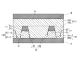
- FIG. 11 is a diagram showing another example 1 of a cross-sectional shape of a printed wiring board.
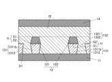
- FIG. 11 is a diagram showing another example 2 of a cross-sectional shape of a printed wiring board.
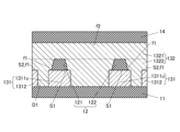
- 13 is a diagram showing another example 3 of a cross-sectional shape of a printed wiring board.
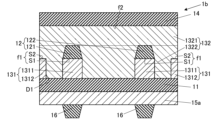
- FIG. 13 is a diagram showing another example 4 of a cross-sectional shape of a printed wiring board.
- FIG. 11 is a table showing the results of calculating differential impedance in a printed wiring board by a numerical simulation.
- FIG. 5 is a diagram showing another example 5 of a cross-sectional shape of a printed wiring board.
- FIG. 13 is a diagram showing another example 6 of a cross-sectional shape of a printed wiring board.
- FIG. 1A is a plan view parallel to the upper surface of a printed wiring board 1 of this embodiment
- FIG. Fig. 1A is a plan view taken along the line BB in Fig. 1B
- Fig. 1B is a cross-sectional view taken along the line AA in Fig. 1A, and includes a conductor layer not shown in Fig. 1A. Note that these figures may show only a portion of the printed wiring board 1. Also, the scale and aspect ratio of each component in these figures are for explanation purposes and do not necessarily reflect the optimal configuration.
- the printed wiring board 1 includes a first ground conductor 11 located on the bottom side, a second ground conductor 14 located on the top side, and wiring 12 and an insulating layer 13 located between the first ground conductor 11 and the second ground conductor 14.
- the first ground conductor 11 and the second ground conductor 14 are solid conductor layers made of metal or the like that include at least a planar perspective position that corresponds to the wiring 12.
- the first ground conductor 11 and the second ground conductor 14 may be made of, for example, copper, aluminum, gold, etc.
- the insulating layer 13 is located on the side of the second ground conductor 14 of the first ground conductor 11.
- the insulating layer 13 includes a first insulating layer 131 and a second insulating layer 132.
- the lower surface of the first insulating layer 131 is in contact with the first ground conductor 11.
- the first insulating layer 131 has a groove D1 having an opening along the extension direction of the wiring 12 in a planar perspective. At least a part of the groove D1 may be a through groove that penetrates the first insulating layer 131 from top to bottom.
- the side wall surface of the groove D1 may be perpendicular to the upper surface of the first ground conductor 11.
- the perpendicular here includes a tilt within the range of error that may occur during manufacturing, for example, a tilt range of about ⁇ 5%, i.e., ⁇ 4.5 degrees or less.
- the first ground conductor 11 may be, for example, copper, aluminum, gold, etc.
- the wiring 12 extends in a first region S1, which is a region of the surface (first surface f1) opposite to the surface in contact with the first ground conductor 11.
- the wiring 12 is not particularly limited, but may be a differential signal wiring in which the first signal wiring conductor 121 and the second signal wiring conductor 122 are positioned parallel to each other. In the differential signal wiring, the distance between the wirings 12 may be, for example, 250 ⁇ m. Both ends of the wiring 12 in the extension direction may be connected to a through conductor such as a through hole or a via.
- the wiring 12 may be curved and/or bent in the middle.
- the wiring 12 may be made of a material having high electrical conductivity, excellent workability, and corrosion resistance, such as copper.
- the wiring 12 has a slightly flattened trapezoidal shape in a cross section perpendicular to the extension direction, but is not limited to this.
- the wiring 12 may also have a rectangular shape, a shape with rounded corners, an ellipse, etc. in a cross section.
- the width of the wiring 12 may be 50 ⁇ m.
- the opening edge of the groove D1 on the first surface f1 may be located along the contours of the first signal wiring conductor 121 and the second signal wiring conductor 122 in planar perspective. Being located along the contours means that the width of the wiring 12 (first region S1) may be equal to the width of the first surface f1, which is the upper surface of a portion 1311 of the first insulating layer 131 in contact with the wiring 12, or the width of the first insulating layer 131 in contact with the wiring 12 may be greater than the width of the wiring 12.
- the entire area between the first signal wiring conductor 121 and the second signal wiring conductor 122 may be a groove D1.
- the groove D1 may not be within a certain distance from the first signal wiring conductor 121 and the second signal wiring conductor 122.
- the first insulating layer 131 has a portion 1312 corresponding to the second region S2 located at a position sandwiching the groove D1 from the portion 1311 corresponding to the first region S1 in planar perspective. That is, the second region S2 (part 1312) is located surrounding the wiring 12 and the groove D1.
- the second insulating layer 132 is located on the first surface f1 of the first insulating layer 131 (part 1311) so as to cover the wiring 12.
- the second insulating layer 132 also includes a first portion 1322 located in the groove D1. That is, the second insulating layer 132 is connected to the portion 1321 covering the side (upper surface) of the first insulating layer 131 opposite to the first ground conductor 11 and the first portion 1322 filling the groove D1. As a result, the second insulating layer 132 is in direct contact with the first ground conductor 11 at the first portion.
- the relative dielectric constant of the second insulating layer 132 is smaller than the relative dielectric constant of the first insulating layer 131 (e.g., about 3.5 to 5.0).
- the second insulating layer 132 may be a liquid crystal polymer (relative dielectric constant is, for example, about 2.8 to 3.3).
- the upper surface of the second insulating layer 132 i.e., the side opposite to the wiring 12 (second surface f2), is in contact with the second ground conductor.
- the first insulating layer 131 and the second insulating layer 132 may each include a glass cloth (not shown).
- the glass cloth extends in the extension direction of each layer corresponding to, for example, the front-rear and left-right directions in FIG. 1B, but the glass cloth in the first insulating layer 131 is interrupted at the groove D1, which is the part corresponding to the first part 1322 in a planar perspective.
- the glass cloth increases the rigidity of the printed wiring board 1 and reduces the thermal expansion coefficient, but has a higher dielectric constant than resin.
- the first insulating layer 131 may be, for example, R-5670 (GC) or R-5670 (GF) of MEGTRON6 manufactured by Panasonic (registered trademark) and may have a thickness of 0.06 mm.
- the second insulating layer 132 may be, for example, R-1551 (MD) manufactured by Panasonic Corporation, and may have a thickness of 0.055 mm.
- the first insulating layer 131 and the second insulating layer 132 may contain an inorganic filler in addition to the above.
- the second insulating layer 132 (first portion 1322) is located within the groove D1 of the first insulating layer 131.
- the conventional insulating layer 13 does not have the groove D1, that is, the insulating layer 13 between the wiring 12 and the first ground conductor 11 is only the first insulating layer 131 with an uninterrupted glass cloth. Therefore, in the present disclosure, the volume ratio of the insulating material with a low relative dielectric constant around the wiring 12 can be increased in the cross-sectional view of FIG. 1B compared to the conventional embodiment. Therefore, this embodiment can mitigate the decrease in characteristic impedance of the wiring 12 more than the conventional embodiment.
- Such a printed wiring board 1 may be obtained, for example, by the following manufacturing procedure.
- a first insulating layer 131 is uniformly formed on the first ground conductor 11, and the wiring 12 is then arranged. After that, unnecessary first insulating layer 131 is removed by laser processing to match the shape of the required groove D1. At this time, the glass cloth in the corresponding area in the first insulating layer 131 is also removed. Then, a second insulating layer is laminated to cover the wiring 12, and at the same time, the groove D1 is filled with the resin of the second insulating layer 132. Next, the second ground conductor 14 is arranged on the second insulating layer 132.
- FIG. 2A, 2B, 3A, and 3B are diagrams showing other examples of the cross-sectional shape shown in FIG. 1B.
- a portion 1311a of the first insulating layer 131 corresponding to the first region S1 may have a width that gradually decreases from the side of the first ground conductor 11 toward the side of the wiring 12.
- the volume ratio of the insulating material with a low relative dielectric constant around the wiring 12 is reduced compared to the case of Fig. 1B. Therefore, the printed wiring board 1 can structurally support the wiring 12 more stably while reducing an increase in characteristic impedance.
- the portion 1311b of the first insulating layer 131 corresponding to the first region S1 may have a width that gradually increases from the side of the first ground conductor 11 toward the side of the wiring 12.
- the width, i.e., the planar area, of a portion 1311c of the first insulating layer 131 including the first surface f1 may be larger than the first region S1, which is the contact surface of the wiring 12 with the first insulating layer 131.
- the width of the wiring 12 and the width of the first surface in contact with the wiring 12 may not be the same.
- a portion 1312d of the first insulating layer 131 corresponding to the second region S2d may be present near the center between the first signal wiring conductor 121 and the second signal wiring conductor 122.
- the groove D11 around the first signal wiring conductor 121 and the groove D12 around the second signal wiring conductor 122 may have a bifurcated portion.
- the width of the groove D1 is narrower than in the above embodiment, the range of a certain distance from the contour of the first signal wiring conductor 121 and the range of a certain distance from the contour of the second signal wiring conductor 122 are separated.
- a portion 1312d of the first insulating layer 131 where no wiring 12 is arranged may be located near the center between the first signal wiring conductor 121 and the second signal wiring conductor 122.
- the bond between the insulating materials of the first insulating layer 131 and the second insulating layer 132 tends to be weaker than the bond between the insulating material and the ground conductor.
- the bond area can be increased, improving the bond strength.
- the glass cloth in the insulating layer 13 remains without being removed in the area where the second insulating layer 132 overlaps with a portion 1312d of the central first insulating layer 131 in a plan view. Therefore, the flow of resin during the formation of the printed wiring board 1 is reduced more than in the above examples 1 to 3, and the misalignment of the wiring between the layers and the decrease in rigidity due to the presence of the groove D12 can be suppressed.
- FIG. 4 is a table showing the results of calculating the characteristic (differential) impedance of printed wiring board 1 of this embodiment by numerical simulation.
- the wiring 12, which is a differential wiring has a first signal wiring conductor 121 and a second signal wiring conductor 122 each having a circuit width of 50 ⁇ m, and a circuit gap between the first signal wiring conductor 121 and the second signal wiring conductor 122 of 250 ⁇ m.
- the thickness of the wiring 12 is 16 ⁇ m.
- the thickness of the first insulating layer 131 is 60 ⁇ m, and the first insulating layer 131 made of resin and glass cloth has a uniform relative dielectric constant of 4.40 throughout.
- the second insulating layer 132 has a thickness of 54 ⁇ m excluding the first portion filling the groove D1, and the second insulating layer 132 made of resin and glass cloth has a uniform relative dielectric constant of 3.26 throughout, and the resin of the second insulating layer 132 has a relative dielectric constant of 3.07.
- the groove D1 is located around each of the wirings 12 along its contour in plan view.
- the width of the groove D1 is 150 ⁇ m at the opening and 130 ⁇ m at the lower end in contact with the first ground conductor 11. That is, the first portion 1322 of the second insulating layer 132 between the first signal wiring conductor 121 and the second signal wiring conductor 122 does not have the portion 1312d of the first insulating layer 131 in Example 4.
- the groove D1 has a tapered shape as a whole as in Example 1.
- the depth of the groove D1 is the same as the thickness of the first insulating layer 131, that is, 60 ⁇ m.
- the simulation was performed using Electronics Pro 2D manufactured by ANSYS.
- the differential impedance of the wiring 12 in the printed wiring board 1 can be set to approximately the target of 100 ⁇ . Since the differential impedance varies by approximately ⁇ 9% during manufacturing, the resulting printed wiring board 1 falls within the range of 90 ⁇ to 110 ⁇ , which is ⁇ 10% of the target of 100 ⁇ . Therefore, the yield during manufacturing of the printed wiring board 1 can be improved.
- Comparative example 1 is a case where the first insulating layer 131 does not have the groove D1. That is, with the plane including the bottom surface of the wiring 12 as the boundary, all of the insulating layer 13 on the side of the first ground conductor 11 from this boundary is the first insulating layer 131, and all of the insulating layer 13 on the side of the second ground conductor 14 from this boundary is the second insulating layer 132.
- the differential impedance does not reach the target of 100 ⁇ , and the overall value is low.
- Comparative Example 2 the circuit width is narrowed to 46 ⁇ m, and the rest of the design is the same as in the Example.
- the median differential impedance is about 100 ⁇ , and the variation is suppressed to within 90 ⁇ to 110 ⁇ , which is ⁇ 10% of 100 ⁇ .
- the circuit gap is expanded to 950 ⁇ m, and other design values are the same as in the Example. Simply widening the circuit gap does not increase the differential impedance sufficiently. Therefore, the median is slightly lower than 100 ⁇ , and within the range of variation, products may be produced that are below 90 ⁇ , which is -10% of 100 ⁇ . Furthermore, the circuit accommodation capacity deteriorates as the circuit gap increases, and the size of the printed wiring board 1 also increases, leading to increased costs and required space.
- FIG. 5A and 5B are diagrams showing other examples of the cross-sectional shape of printed wiring board 1.
- FIG. 5A As in the printed wiring board 1a of Example 5 shown in FIG. 5A, a plurality of stripline structures may be laminated.
- the lamination order (upper-lower relationship) of the first insulating layer 131 and the second insulating layer 132 may be different between the insulating layers 13 relating to the plurality of stripline structures.
- the wiring 12 is overlapped and positioned at the same position in a planar perspective here, this is not limited to this.
- the position of the wiring 12 may be different between the plurality of insulating layers 13.
- the insulating layer 15 positioned between the plurality of stripline structures may be made of the same material as the first insulating layer 131, or may be made of the same material as the second insulating layer 132 having a low relative dielectric constant.
- wiring 16 connected to the stripline structure or separate wiring 16 may be exposed on the outer surface of printed wiring board 1.
- This wiring 16 may be covered with a protective film or the like.
- the printed wiring board 1 may be used as a core substrate, with a build-up layer or the like located on one or both sides of the core substrate.
- a solder resist layer may also be located on the outer surface of the printed wiring board 1.
- the printed wiring board 1 of the present embodiment includes the first ground conductor 11, the first insulating layer 131 located on the first ground conductor 11 and having a first surface f1 on the opposite side to the first ground conductor 11, the wiring 12 extending over the first region S1 of the first surface f1, the second insulating layer 132 located on the first surface f1 to cover the wiring 12 and having a second surface f2 on the opposite side to the first insulating layer 131, and the second ground conductor 14 located on the second surface f2.
- the first insulating layer 131 has a groove D1 having an opening that is at least along the direction in which the wiring 12 on the first surface f1 extends in a planar perspective view.
- the second insulating layer 132 has a first portion 1322 located in the groove D1.
- the relative dielectric constant of the second insulating layer 132 is smaller than the relative dielectric constant of the first insulating layer 131.
- the groove D1 may be located around the wiring 12, and the opening edge of the groove D1 may be located along the contour of the wiring 12 in a planar perspective.
- the printed wiring board 1 can control the characteristic impedance over a wider range.
- At least a portion of the groove D1 may be a through groove penetrating the first insulating layer 131.
- the first portion 1322 of the second insulating layer 132 may be in contact with the first ground conductor 11. This allows the printed wiring board 1 to control the characteristic impedance over a wider range even though it is small and thin.
- the second insulating layer 132 is in direct contact with the first ground conductor 11, it is easier to increase the bonding strength than when the second insulating layer 132 is bonded to the first insulating layer 131. Therefore, the printed wiring board 1 can improve the robustness and durability of the structure.
- the wiring 12 may also include differential signal wiring in which the first signal wiring conductor 121 and the second signal wiring conductor 122 are positioned next to each other.
- the groove D1 is positioned around and between the first signal wiring conductor 121 and the second signal wiring conductor 122.
- the second insulating layer 132 which has a relatively low dielectric constant, is positioned between the two differential signal wirings, so that the characteristic impedance of the wiring 12 can be set to a value within an appropriate range even if the interlayer distance is small.
- the first surface f1 may include a second region S2 (an upper surface of a portion 1312 of the first insulating layer 131) in which the wiring 12 is not located.
- the first region S1 and the second region S2 may be located with an opening (groove D1) therebetween. Therefore, first portion 1322 having a low dielectric constant is surrounded by portion 1312 of first insulating layer 131, improving the bonding strength between the insulating layers, and allowing printed wiring board 1 to have a stable shape.
- the sidewall surface of the groove D1 that follows the contour of the wiring 12 may be perpendicular to the first ground conductor 11.
- the portion 1311 of the first insulating layer 131 from becoming unnecessarily thick, a more stable and appropriate characteristic impedance can be obtained.
- the portion 1311 from becoming unnecessarily thin the wiring 12 can be reliably supported and the wiring is less likely to collapse during manufacturing.
- the width of the wiring 12 in contact with the first region S1 and the width of the first surface, which is the upper surface of the portion 1311 of the first insulating layer 131 in contact with the wiring 12, may be equal.
- the portion 1311 of the first insulating layer 131 does not become unnecessarily thick, so that an appropriate characteristic impedance can be obtained.
- “equal” here includes the width of the error that may occur during manufacturing, for example, the difference between the width of the wiring 12 in contact with the first region S1 and the width of the first insulating layer 131 in contact with the wiring 12 being about ⁇ 30% or less of the width of the wiring 12.
- the wiring 12 does not have to be a differential signal wiring, and may be a wiring that transmits one or more signals independently, such as a signal or power.
- groove D1 is described as being a through groove, but it does not necessarily have to be a through groove. Also, only a portion of it may be a through groove, with the remaining portion being a non-through groove. As described above, it is difficult to increase the bonding strength between different insulating layers, but by increasing the unevenness of the contact surface, the overall bonding strength can be improved.
- the first insulating layer 131 is described as having a portion 1312 that corresponds to the second region S2, but this is not necessary.
- the first insulating layer 131 may have only a portion 1311 that corresponds to the first region S1.
- the cross-sectional shape of the side wall surface may be different between a portion 1311 and another portion 1312 of the first insulating layer 131. Alternatively, the same portion may have a portion whose side wall surface has a different cross-sectional shape. Furthermore, each cross-sectional shape does not have to be linear.
- the specific configurations, structures, materials, sizes, manufacturing procedures, etc. shown in the above embodiments can be modified as appropriate without departing from the spirit of the present invention. The scope of the present invention includes the scope of the invention described in the claims and its equivalents.
- This disclosure can be used for printed wiring boards.
Landscapes
- Engineering & Computer Science (AREA)
- Manufacturing & Machinery (AREA)
- Microelectronics & Electronic Packaging (AREA)
- Structure Of Printed Boards (AREA)
Priority Applications (1)
| Application Number | Priority Date | Filing Date | Title |
|---|---|---|---|
| JP2024574848A JP7817459B2 (ja) | 2023-01-31 | 2024-01-26 | 印刷配線板 |
Applications Claiming Priority (2)
| Application Number | Priority Date | Filing Date | Title |
|---|---|---|---|
| JP2023-012570 | 2023-01-31 | ||
| JP2023012570 | 2023-01-31 |
Publications (1)
| Publication Number | Publication Date |
|---|---|
| WO2024162191A1 true WO2024162191A1 (ja) | 2024-08-08 |
Family
ID=92146707
Family Applications (1)
| Application Number | Title | Priority Date | Filing Date |
|---|---|---|---|
| PCT/JP2024/002344 Ceased WO2024162191A1 (ja) | 2023-01-31 | 2024-01-26 | 印刷配線板 |
Country Status (3)
| Country | Link |
|---|---|
| JP (1) | JP7817459B2 (https=) |
| TW (1) | TW202435672A (https=) |
| WO (1) | WO2024162191A1 (https=) |
Citations (3)
| Publication number | Priority date | Publication date | Assignee | Title |
|---|---|---|---|---|
| JPH0341803A (ja) * | 1989-07-07 | 1991-02-22 | Hitachi Chem Co Ltd | 信号線相互間のクロストークノイズを低減した配線板およびその製造法 |
| JP2006245291A (ja) * | 2005-03-03 | 2006-09-14 | Nec Corp | 伝送線路及び配線形成方法 |
| JP2017108455A (ja) * | 2014-09-26 | 2017-06-15 | 株式会社村田製作所 | 伝送線路および電子機器 |
Family Cites Families (1)
| Publication number | Priority date | Publication date | Assignee | Title |
|---|---|---|---|---|
| WO2022124179A1 (ja) | 2020-12-07 | 2022-06-16 | 株式会社村田製作所 | 回路基板及び回路基板の製造方法 |
-
2024
- 2024-01-26 JP JP2024574848A patent/JP7817459B2/ja active Active
- 2024-01-26 WO PCT/JP2024/002344 patent/WO2024162191A1/ja not_active Ceased
- 2024-01-30 TW TW113103566A patent/TW202435672A/zh unknown
Patent Citations (3)
| Publication number | Priority date | Publication date | Assignee | Title |
|---|---|---|---|---|
| JPH0341803A (ja) * | 1989-07-07 | 1991-02-22 | Hitachi Chem Co Ltd | 信号線相互間のクロストークノイズを低減した配線板およびその製造法 |
| JP2006245291A (ja) * | 2005-03-03 | 2006-09-14 | Nec Corp | 伝送線路及び配線形成方法 |
| JP2017108455A (ja) * | 2014-09-26 | 2017-06-15 | 株式会社村田製作所 | 伝送線路および電子機器 |
Also Published As
| Publication number | Publication date |
|---|---|
| JP7817459B2 (ja) | 2026-02-18 |
| JPWO2024162191A1 (https=) | 2024-08-08 |
| TW202435672A (zh) | 2024-09-01 |
Similar Documents
| Publication | Publication Date | Title |
|---|---|---|
| US9674941B2 (en) | Printed circuit board for mobile platforms | |
| EP2785155B1 (en) | Circuit board and electronic device | |
| JPWO2020130010A1 (ja) | 伝送線路部材 | |
| CN103260339A (zh) | 多层布线板和电子装置 | |
| JP6151794B2 (ja) | 回路基板、電子部品収納用パッケージおよび電子装置 | |
| CN116209138B (zh) | 电路板与其制造方法 | |
| KR101439089B1 (ko) | 다층 쓰루홀 적층 구조체 | |
| US20060285273A1 (en) | Composite distributed dielectric structure | |
| JP4848490B2 (ja) | 伝送線路及びこれを有する配線基板並びに半導体装置 | |
| US8841561B1 (en) | High performance PCB | |
| TWM540453U (zh) | 軟式印刷電路板與硬式印刷電路板焊接結構 | |
| JP7817459B2 (ja) | 印刷配線板 | |
| JP7574863B2 (ja) | 回路基板 | |
| CN114828399B (zh) | 共轴通孔结构 | |
| JP6465451B1 (ja) | 電子回路 | |
| JP7197057B2 (ja) | 伝送線路 | |
| JP7455730B2 (ja) | 配線基板 | |
| JP6491080B2 (ja) | 多層配線基板 | |
| US20220346231A1 (en) | Printed wiring board | |
| WO2025089165A1 (ja) | 配線基板およびそれを用いた実装構造体 | |
| TWI684245B (zh) | 差動訊號傳輸電路板 | |
| JP2024134851A (ja) | 大判配線基板 | |
| CN120711602A (zh) | 折叠式电路板及其制造方法 | |
| WO2023204099A1 (ja) | 多層基板 | |
| JP2024098882A (ja) | 樹脂多層基板及び電子部品 |
Legal Events
| Date | Code | Title | Description |
|---|---|---|---|
| 121 | Ep: the epo has been informed by wipo that ep was designated in this application |
Ref document number: 24750140 Country of ref document: EP Kind code of ref document: A1 |
|
| ENP | Entry into the national phase |
Ref document number: 2024574848 Country of ref document: JP Kind code of ref document: A |
|
| WWE | Wipo information: entry into national phase |
Ref document number: 2024574848 Country of ref document: JP |
|
| NENP | Non-entry into the national phase |
Ref country code: DE |
|
| 122 | Ep: pct application non-entry in european phase |
Ref document number: 24750140 Country of ref document: EP Kind code of ref document: A1 |