EP2785155B1 - Circuit board and electronic device - Google Patents
Circuit board and electronic device Download PDFInfo
- Publication number
- EP2785155B1 EP2785155B1 EP14160209.4A EP14160209A EP2785155B1 EP 2785155 B1 EP2785155 B1 EP 2785155B1 EP 14160209 A EP14160209 A EP 14160209A EP 2785155 B1 EP2785155 B1 EP 2785155B1
- Authority
- EP
- European Patent Office
- Prior art keywords
- electrodes
- circuit board
- pair
- signal
- ground
- Prior art date
- Legal status (The legal status is an assumption and is not a legal conclusion. Google has not performed a legal analysis and makes no representation as to the accuracy of the status listed.)
- Not-in-force
Links
Images


Classifications
-
- H—ELECTRICITY
- H05—ELECTRIC TECHNIQUES NOT OTHERWISE PROVIDED FOR
- H05K—PRINTED CIRCUITS; CASINGS OR CONSTRUCTIONAL DETAILS OF ELECTRIC APPARATUS; MANUFACTURE OF ASSEMBLAGES OF ELECTRICAL COMPONENTS
- H05K1/00—Printed circuits
- H05K1/02—Details
- H05K1/0213—Electrical arrangements not otherwise provided for
- H05K1/0216—Reduction of cross-talk, noise or electromagnetic interference
- H05K1/0218—Reduction of cross-talk, noise or electromagnetic interference by printed shielding conductors, ground planes or power plane
- H05K1/0219—Printed shielding conductors for shielding around or between signal conductors, e.g. coplanar or coaxial printed shielding conductors
- H05K1/0222—Printed shielding conductors for shielding around or between signal conductors, e.g. coplanar or coaxial printed shielding conductors for shielding around a single via or around a group of vias, e.g. coaxial vias or vias surrounded by a grounded via fence
-
- H—ELECTRICITY
- H05—ELECTRIC TECHNIQUES NOT OTHERWISE PROVIDED FOR
- H05K—PRINTED CIRCUITS; CASINGS OR CONSTRUCTIONAL DETAILS OF ELECTRIC APPARATUS; MANUFACTURE OF ASSEMBLAGES OF ELECTRICAL COMPONENTS
- H05K1/00—Printed circuits
- H05K1/02—Details
- H05K1/0213—Electrical arrangements not otherwise provided for
- H05K1/0237—High frequency adaptations
- H05K1/025—Impedance arrangements, e.g. impedance matching, reduction of parasitic impedance
- H05K1/0251—Impedance arrangements, e.g. impedance matching, reduction of parasitic impedance related to vias or transitions between vias and transmission lines
-
- H—ELECTRICITY
- H01—ELECTRIC ELEMENTS
- H01L—SEMICONDUCTOR DEVICES NOT COVERED BY CLASS H10
- H01L2224/00—Indexing scheme for arrangements for connecting or disconnecting semiconductor or solid-state bodies and methods related thereto as covered by H01L24/00
- H01L2224/01—Means for bonding being attached to, or being formed on, the surface to be connected, e.g. chip-to-package, die-attach, "first-level" interconnects; Manufacturing methods related thereto
- H01L2224/10—Bump connectors; Manufacturing methods related thereto
- H01L2224/15—Structure, shape, material or disposition of the bump connectors after the connecting process
- H01L2224/16—Structure, shape, material or disposition of the bump connectors after the connecting process of an individual bump connector
-
- H—ELECTRICITY
- H01—ELECTRIC ELEMENTS
- H01L—SEMICONDUCTOR DEVICES NOT COVERED BY CLASS H10
- H01L2924/00—Indexing scheme for arrangements or methods for connecting or disconnecting semiconductor or solid-state bodies as covered by H01L24/00
- H01L2924/15—Details of package parts other than the semiconductor or other solid state devices to be connected
- H01L2924/151—Die mounting substrate
- H01L2924/1517—Multilayer substrate
- H01L2924/15172—Fan-out arrangement of the internal vias
- H01L2924/15174—Fan-out arrangement of the internal vias in different layers of the multilayer substrate
-
- H—ELECTRICITY
- H01—ELECTRIC ELEMENTS
- H01L—SEMICONDUCTOR DEVICES NOT COVERED BY CLASS H10
- H01L2924/00—Indexing scheme for arrangements or methods for connecting or disconnecting semiconductor or solid-state bodies as covered by H01L24/00
- H01L2924/15—Details of package parts other than the semiconductor or other solid state devices to be connected
- H01L2924/151—Die mounting substrate
- H01L2924/153—Connection portion
- H01L2924/1531—Connection portion the connection portion being formed only on the surface of the substrate opposite to the die mounting surface
- H01L2924/15311—Connection portion the connection portion being formed only on the surface of the substrate opposite to the die mounting surface being a ball array, e.g. BGA
-
- H—ELECTRICITY
- H05—ELECTRIC TECHNIQUES NOT OTHERWISE PROVIDED FOR
- H05K—PRINTED CIRCUITS; CASINGS OR CONSTRUCTIONAL DETAILS OF ELECTRIC APPARATUS; MANUFACTURE OF ASSEMBLAGES OF ELECTRICAL COMPONENTS
- H05K1/00—Printed circuits
- H05K1/02—Details
- H05K1/0213—Electrical arrangements not otherwise provided for
- H05K1/0216—Reduction of cross-talk, noise or electromagnetic interference
- H05K1/0228—Compensation of cross-talk by a mutually correlated lay-out of printed circuit traces, e.g. for compensation of cross-talk in mounted connectors
-
- H—ELECTRICITY
- H05—ELECTRIC TECHNIQUES NOT OTHERWISE PROVIDED FOR
- H05K—PRINTED CIRCUITS; CASINGS OR CONSTRUCTIONAL DETAILS OF ELECTRIC APPARATUS; MANUFACTURE OF ASSEMBLAGES OF ELECTRICAL COMPONENTS
- H05K1/00—Printed circuits
- H05K1/02—Details
- H05K1/0213—Electrical arrangements not otherwise provided for
- H05K1/0216—Reduction of cross-talk, noise or electromagnetic interference
- H05K1/023—Reduction of cross-talk, noise or electromagnetic interference using auxiliary mounted passive components or auxiliary substances
- H05K1/0231—Capacitors or dielectric substances
-
- H—ELECTRICITY
- H05—ELECTRIC TECHNIQUES NOT OTHERWISE PROVIDED FOR
- H05K—PRINTED CIRCUITS; CASINGS OR CONSTRUCTIONAL DETAILS OF ELECTRIC APPARATUS; MANUFACTURE OF ASSEMBLAGES OF ELECTRICAL COMPONENTS
- H05K1/00—Printed circuits
- H05K1/02—Details
- H05K1/11—Printed elements for providing electric connections to or between printed circuits
- H05K1/115—Via connections; Lands around holes or via connections
-
- H—ELECTRICITY
- H05—ELECTRIC TECHNIQUES NOT OTHERWISE PROVIDED FOR
- H05K—PRINTED CIRCUITS; CASINGS OR CONSTRUCTIONAL DETAILS OF ELECTRIC APPARATUS; MANUFACTURE OF ASSEMBLAGES OF ELECTRICAL COMPONENTS
- H05K2201/00—Indexing scheme relating to printed circuits covered by H05K1/00
- H05K2201/10—Details of components or other objects attached to or integrated in a printed circuit board
- H05K2201/10613—Details of electrical connections of non-printed components, e.g. special leads
- H05K2201/10621—Components characterised by their electrical contacts
- H05K2201/10734—Ball grid array [BGA]; Bump grid array
Definitions
- the embodiment discussed herein is related to a circuit board and an electronic device.
- Circuit boards on which various components are mounted have been widely used for electronic devices.
- an electronic device a semiconductor package
- a circuit board a package substrate
- an electronic device includes a circuit board, such as a mother board, on which a semiconductor package is mounted.
- a differential transmission type circuit board as a circuit board has been used, signals in the differential transmission type circuit are transmitted through a pair of transmission paths.
- US 2012/0247825 discloses a printed circuit board including a top signal layer, a bottom signal layer, a ground layer, a plurality of vias and at least two ground vias.
- circuit board as defined in claim 1.
- Preferred features are defined in the dependent claims.
- FIG. 1 is a diagram illustrating an example electronic device. Specifically, FIG. 1 is a cross-sectional view illustrating a major part of an example electronic device.
- An electronic device 100a illustrated in FIG. 1 includes a package substrate (a circuit board) 200, a semiconductor element 300 mounted on the package substrate 200, and a mother board (a circuit board) 400 connected to the package substrate 200 on which the semiconductor element 300 is mounted.
- the package substrate 200 is, for example, a build-up circuit board, and includes a core layer 210, and wire layers 220 and 230 formed on front and back surfaces of the core layer 210 using a build-up technology.
- a through hole via 211 is provided in the core layer 210 of the package substrate 200.
- a via 221 and a wire 222 are provided in a wire layer 220 provided on one side of the core layer 210 so as to be electrically connected to the through hole via 211 of the core layer 210, and an electrode 223 is provided on a surface of the wire layer 220 so as to be located in a position corresponding to an electrode 310 of the semiconductor element 300.
- a via 231 and a wire 232 are provided in a wire layer 230 provided on the other side of the core layer 210 so as to be electrically connected to the through hole via 211 of the core layer 210, and an electrode 233 is provided on a surface of the wire layer 230 so as to be located in a position corresponding to an electrode 410 of the mother board 400.
- the semiconductor element 300 is mounted on the package substrate 200 configured in the above-described manner.
- the electrode 310 of the semiconductor element 300 and the electrode 223 of the package substrate 200 are joined together via a bump 320, and thus, the semiconductor element 300 is mounted on the package substrate 200.
- the semiconductor element 300 is mounted on the package substrate 200 to form a semiconductor package 110a.
- the electrode 233 of the package substrate 200 of the semiconductor package 110a is connected to the electrode 410 of the mother board 400 via a bump 120, and thus, the semiconductor package 110a is mounted on the mother board 400.
- a laminated body of prepreg 420 may be used as the mother board 400, where the laminated body of prepreg 420 includes a conductor pattern 420a provided on both of front and back surfaces thereof, or the front surface or the back surface thereof may.
- a through hole 430 is formed so that the front surface of the mother board 400 is electrically connected to the back surface thereof.
- FIG. 1 illustrates as an example a case where an AC coupling capacitor 500 is bonded, via a solder 510, to a transmission path of the mother board 400 through which the relatively high frequency signal is transmitted.
- some of the electronic device may use a circuit board, in which transmits a relatively high frequency signal, including a pair of transmission paths (pair transmission paths) through which a signal is transmitted by a differential transmission method.
- a circuit board in which transmits a relatively high frequency signal, including a pair of transmission paths (pair transmission paths) through which a signal is transmitted by a differential transmission method.
- crosstalk an electromagnetic interference
- One of methods for reducing crosstalk is to provide an electromagnetic shielding structure using a conductor body at a ground potential between the different pairs of transmission paths in the circuit board.
- signal electrodes extended from the pair transmission paths are exposed on a surface of the circuit board, and therefore, crosstalk might occur in a joint part where the signal electrode and an electrode of a component joined to the circuit board are joined together.
- FIGs. 2A-2B , FIG. 3 , and FIG. 4 are diagrams illustrating an example circuit board.
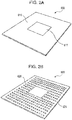
- FIGs. 2A-2B illustrate, as an example circuit board, a package substrate 600 on which a semiconductor element is mounted.
- a mounting area 611 for a semiconductor element is provided on one surface 610 of the package substrate 600 illustrated in FIG. 2A .
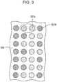
- the group of electrodes 621 arranged in the latticed pattern as illustrated in FIG. 2B includes signal electrodes extending from pairs of wires (pair wires) provided in the package substrate 600.
- the group of electrodes 621 includes pairs of signal electrodes 621a (a single pair is surrounded by a dashed line in FIG. 3 ) and ground electrodes 621b, and these electrodes are mixedly arranged in the latticed pattern on the surface 620 of the package substrate 600.
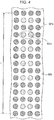
- ground electrodes 621b are disposed between the different pairs of signal electrodes 621a (a single pair is surrounded by a dashed line in FIG. 4 ), and thus, a certain distance is ensured between the different pairs of signal electrodes 621a.
- the number of groups of electrodes 621 (including the signal electrodes 621a and the ground electrodes 621b) arranged on the surface 620 of the package substrate 600 is increased, and accordingly, an arrangement area of the group of electrodes 621 is increased. If the number of pins provided in the semiconductor element which is mounted on the electronic device is increased because of the demand for high performance, the number of the groups of electrodes 621 and the arrangement area thereof are increased for the purpose of reducing crosstalk, thus increasing the number of pins provided on the package substrate 600 and the size of the package substrate 600.
- the group of electrodes 621 is provided with reduced intervals to increase arrangement density, thereby reducing increase in size of the package substrate 600 due to increase in the number of pins and also reducing a wire length.
- crosstalk is not effectively reduced, and furthermore, in the electrode arrangement illustrated in FIG. 4 , although a certain crosstalk reduction effect is achieved, there is a probability that the number of pins provided in the package substrate 600 and the size of the package substrate 600 are increased, the wire length is increased, and thus, transmission loss is increased.
- FIG. 5 is a diagram illustrating a first example of electrode arrangement. Specifically, FIG. 5 is a schematic view of an example electrode arrangement in a part of an area of a circuit board.
- a circuit board 10 illustrated in FIG. 5 includes, in a part of the surface 11, four ground electrodes 21 disposed at vertexes of a rectangular area 20A indicated by dashed lines and a pair of signal electrodes 22 disposed in the rectangular area 20A and surrounded by the ground electrodes 21.
- the circuit board 10 is, for example, a package substrate.
- the package substrate include various types of substrate, such as, a build-up substrate, a ceramic substrate, a glass ceramic substrate, a coreless substrate, and the like.
- a surface 11 of the circuit board 10 on which the ground electrodes 21 and the signal electrodes 22 are disposed is, for example, a surface which is joined to another component, such as a mother board, and the like.
- the ground electrodes 21 are electrodes which have a potential serving as a ground potential of the circuit board 10
- the pair of signal electrodes 22 is electrodes each of which is electrically connected to the corresponding one of pair wires provided in the circuit board 10.
- the pair of signal electrodes 22 is arranged in a direction S which is parallel to a side 23 of the rectangular area 20A with an interval a (with a distance (a pitch) a) between respective centers of the pair of signal electrodes 22).
- the rectangular area 20A has, for example, a square shape.
- the four ground electrodes 21 are disposed at the vertexes of the rectangular area 20A having a square shape with intervals b (with a pitch b between respective centers of the adjacent ones of the ground electrodes 21) which are greater than the interval a between the pair of signal electrodes 22.
- an electrode arrangement is employed in which the pair of signal electrodes 22 disposed in line in the direction S is surrounded by the four ground electrodes 21 disposed at the vertexes of the rectangular area 20A having a square shape.
- FIG. 6 is a diagram illustrating an example joint part where a circuit board and a component are joined together.
- FIG. 6 is a perspective view schematically illustrating an example joint part where a circuit board and a mother board are joined together.
- the four ground electrodes 21 and the pair of signal electrodes 22 are provided on the surface of the circuit board 10 in the basis of the electrode arrangement illustrated in FIG. 5 .
- Each of vias 15 provided in the circuit board 10 is coupled to the corresponding one of the ground electrodes 21 and the signal electrodes 22.
- a pair of signal wires (pair wires) 16 provided in the circuit board 10 is connected to the vias 15 connected to the pair of signal electrodes 22.
- Each of the ground electrodes 21 and the signal electrodes 22 configured in the above-described manner is joined to the corresponding one of ground electrodes 61 and signal electrodes 62 provided on the surface of the mother board via the corresponding one of bumps 60.
- Each of the vias 63 provided in the mother board is coupled to the corresponding one of the ground electrodes 61 and signal electrodes 62.
- Signal wires 64 provided in the mother board are coupled to the vias 63 electrically connected to the signal electrodes 22.
- the circuit board 10 including the electrode arrangement illustrated in FIG. 5 is, for example, connected to the mother board in the manner illustrated in FIG. 6 .
- the joint parts where the signal electrodes 22 of the circuit board 10 and the signal electrodes 62 of the mother board are connected together are surrounded by the joint parts where the ground electrodes 21 of the circuit board 10 and the ground electrodes 61 of the mother board are joined together, thus reducing crosstalk in the joint parts where the signal electrodes 22 and the signal electrodes 62 are joined together.
- the electrode arrangement illustrated in FIG. 5 may be provided on a plurality of parts of the surface 11 of the circuit board 10.
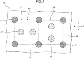
- FIG. 7 is a diagram illustrating a second electrode arrangement example. Specifically, FIG. 7 is a schematic view of an example of an electrode arrangement in an area of a circuit board.
- FIG. 7 illustrates, as an example, the circuit board 10 on which the above-described electrode arrangement illustrated in FIG. 5 is provided on two adjacent parts of the surface 11.
- the circuit board 10 illustrated in FIG. 7 includes, in the surface 11, the ground electrodes 21 disposed at the vertexes of the rectangular area 20A and the pair of signal electrodes 22 disposed in the rectangular area 20A so as to be arranged in the direction S.
- the circuit board 10 illustrated in FIG. 7 includes, in the surface 11, four ground electrodes 21 disposed at vertexes of a rectangular area 20B located adjacent to the rectangular area 20A and a pair of signal electrodes 22 disposed in the rectangular area 20B.
- the pair of signal electrodes 22 disposed in the rectangular area 20B is arranged in a direction T which is parallel to a side 24 of the rectangular area 20B and is perpendicular to the direction S.
- the pair of ground electrodes 21 disposed in the rectangular area 20A so as to be arranged in the direction T and the pair of ground electrodes 21 disposed in the rectangular area 20B so as to be arranged in the direction T are common.
- the two pairs of signal electrodes 22 are arranged in the direction S and the direction T which are perpendicular to each other, and thus, as compared to the case where the two pairs are arranged in the same direction, the two pairs of signal electrodes 22 may be disposed with an increased distance between the two pairs.
- FIG. 8 is an explanatory diagram illustrating a third electrode arrangement example.
- FIG. 8 is a schematic view of an example electrode arrangement in an area of a circuit board.
- FIG. 8 illustrates, as an example, the circuit board 10 on which multiple ones of the electrode arrangement illustrated in FIG. 7 are provided in combination on the surface 11 such that some of the pairs of ground electrodes 21 are shared.
- the ground electrodes 21 and the signal electrodes 22 are disposed such that each of the directions (the directions U and V indicated by dashed lines in FIG. 8 ) in which the pairs of the signal electrodes 22 are arranged is a direction which is neither parallel to an end side 12 of the circuit board 10 nor perpendicular to the end side 12.
- the ground electrodes 21 and the signal electrodes 22 are disposed on the circuit board 10 such that each of the directions U and V in which the pairs of the signal electrodes 22 are arranged intersects the end side 12 at an acute angle of ⁇ .
- the ground electrodes 21 and the signal electrodes 22 are arranged such that the directions U and V in which the pairs of the signal electrodes 22 are arranged form an equal angle ⁇ , that is, 45 degrees, with the end side 12 of the circuit board 10.
- ground electrodes 21 and the signal electrodes 22 as illustrated in FIG. 8 , as compared to the electrode arrangement of the latticed pattern illustrated in FIG. 4 , it may be achieved to reduce the number of ground electrodes 21 disposed in order to surround a certain number of pairs of signal electrodes 22.
- FIG. 8 illustrates a case where seven pairs of signal electrodes 22 are arranged.
- the length L of an electrode arrangement area may be reduced by about 20%, as compared to the case where seven pairs of signal electrodes 621a are arranged as illustrated in FIG. 4 .
- FIG. 9 is an explanatory diagram illustrating a fourth electrode arrangement example.
- FIG. 9 is a schematic plan view of a circuit board viewed from one surface side of the circuit board.
- FIG. 9 illustrates, as an example, the circuit board 10 on which a plurality of electrodes according to the electrode arrangement illustrated in FIG. 8 is provided in a peripheral part 13 of the surface 11.
- a group of electrodes 30 is arranged in a latticed pattern in a further inner area than the peripheral part 13 in the circuit board 10.
- pairs of signal electrodes 22 in the peripheral part 13 as in the circuit board 10 illustrated in FIG. 9 , it may be reduced to occur a worse situation where wires extended from the pairs of signal electrodes 22 are located close to other electrodes (signal electrodes) , and thus, crosstalk may be reduced.
- the number of ground electrodes 21 surrounding a certain number of pairs of signal electrodes 22 may be reduced, as compared to the case ( FIG. 4 ) where the signal electrodes 22 and the ground electrodes 21 are arranged in a latticed pattern.
- the peripheral part 13 of the circuit board 10 in the electrode arrangement illustrated in FIG. 9 , when a certain number of pairs of signal electrodes 22 are provided in the peripheral part 13, the length of the electrode arrangement area may be reduced, as compared to the case ( FIG. 4 ) where the pairs of signal electrodes 22 are arranged in a latticed pattern with the ground electrodes 21.
- circuit board 10 illustrated in FIG. 9 it may be achieved to reduce crosstalk in the joint parts where the circuit board 10 and the mother board are joined together via the signal electrodes 22 by the reduced number of the ground electrodes 21 provided around the signal electrodes 22. Furthermore, it may be achieved to reduce the length of the arrangement area in the peripheral part 13 in which the ground electrodes 21 and the signal electrodes 22 are arranged. Accordingly, the overall size of the circuit board 10 may be reduced. The reduction in overall size of the circuit board 10 enables reduction in length of wires extended from the signal electrodes 22, and thus, when the circuit board 10 is used in transmitting a relatively high frequency signal, transmission loss may be reduced.
- power supply electrodes are disposed as electrodes 30 in a further inner area than the peripheral part 13.
- the electrodes for use in transmitting a relatively high frequency signal and electrodes for a relatively low frequency signal are arranged in the circuit board 10
- the electrodes for use in transmitting a relatively high frequency signal are disposed as the signal electrodes 22 in the peripheral part 13 and the electrodes for use in transmitting relatively low frequency signals are disposed as the electrodes 30 in a further inner side than the peripheral part 13.
- a group of the electrodes 30 located in a central part of the circuit board 10 may include, in addition to the power supply electrode, signal electrodes for use in transmitting signals.
- the electrodes 30 may be arranged in a latticed pattern, as illustrated in FIG. 9 .
- the electrodes 30 are arranged in a latticed pattern with the same intervals as or substantially the same intervals as the interval a between a pair of signal electrodes 22 arranged in the peripheral part 13.
- the electrodes 30 may be arranged with higher density in the central part, as compared to the electrode arrangement in the peripheral part 13.
- FIG. 9 explanatory illustrates a configuration of a non-electrode formation area, in the central part of the surface 11 of the circuit board 10, without forming the group of electrodes 30, the circuit board 10 may be configured such that the electrodes 30 are arranged in a latticed pattern in the central part of the surface 11.
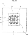
- FIG. 10 is a diagram illustrating a fifth electrode arrangement example. Specifically, FIG. 10 is a schematic plan view of a circuit board viewed from the other surface side of the circuit board.
- FIG. 10 illustrates as an example a configuration in which the above-described electrode arrangement illustrated in FIG. 8 is employed for a semiconductor element mounting area 14a provided in a surface 14 of the circuit board 10 on which a semiconductor element is mounted.
- multiple ones of an electrode arrangement in which a pair of signal electrodes 22 is surrounded by four ground electrodes 21 disposed at vertexes of a rectangular area are provided in combination in a peripheral part 14aa such that some of the pairs of ground electrodes 21 are shared.
- Adjacent pairs of signal electrodes 22 are arranged such that the direction in which one of the adjacent pairs of signal electrodes 22 is perpendicular to the direction in which the other one of the adjacent pairs.
- the pairs of signal electrodes 22 are disposed in the mounting area 14a such that the direction in which each pair is arranged forms an equal angle (45 degrees) with an end side 14ab of the mounting area 14a.
- Power supply electrodes and signal electrodes for use in transmitting relatively low frequency signals may be provided in a further inner area than the peripheral part 14aa in the mounting area 14a so as to be arranged in a latticed pattern.
- the number of the ground electrodes 21 provided around the signal electrodes 22 may be reduced, thus, enabling reduction of crosstalk in the joint parts where the circuit board 10 and the semiconductor element are joined together via the signal electrodes 22. Furthermore, by using the electrode arrangement illustrated in FIG. 10 , the size of the mounting area 14a may be reduced, and the length of each wire provided in the circuit board 10 may be reduced.
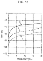
- FIG. 11 is a diagram illustrating a simulation of crosstalk
- FIG. 12 and FIG. 13 are graphs illustrating example simulation results.
- a transmission path between a port 1 and a port 2 is a reference transmission path 5 and a transmission path between a port 3 and a port 4 is an evaluation target transmission path 6, crosstalk which the evaluation target transmission path 6 receives from the reference transmission path 5 is evaluated.
- the transmission path 5 and the transmission path 6 are joint parts (joint parts of different pairs) where the signal electrodes 22 (which correspond to the port 1 and port 3) of the circuit board 10 and electrodes (which correspond to the port 2 and the port 4) of a component, such as a mother board, are joined together.
- a near-end crosstalk (Sdd31) between the port 1 and the port 3 and a far-end crosstalk (Sdd41) between the port 1 and the port 4 are evaluated.
- FIG. 12 and FIG. 13 illustrate an example of the relationship between a transmission signal frequency [GHz] obtained by the simulation and the near-end crosstalk Sdd31 [dB] and an example of the relationship between the transmission signal frequency [GHz] and the far-end crosstalk Sdd41 [dB], respectively.
- Each of FIG. 12 and FIG. 13 indicates a result X obtained when the electrode arrangement of FIG. 3 was employed for the transmission path 5 and the transmission path 6, a result Y obtained when the electrode arrangement of FIG. 4 was employed for the transmission path 5 and the transmission path 6, and a result Z obtained when the electrode arrangement of FIG. 8 was employed for the transmission path 5 and the transmission path 6.
- the near-end crosstalk Sdd31 and the far-end crosstalk Sdd41 may be reduced by employing the electrode arrangement of FIG. 4 for the electrode arrangement of FIG. 3 (the result X and Y). It is also understood from FIG. 12 and FIG. 13 that, when the electrode arrangement of FIG. 8 is employed, the near-end crosstalk Sdd31 and the far-end crosstalk Sdd41 may be further reduced, as compared those when the electrode arrangement of FIG. 4 is employed (the result Y and Z).
- the circuit board 10 including an electrode arrangement which enables reduction of crosstalk in joint parts where the circuit board 10 and a component, such as a mother board and a semiconductor element has been described above.
- a component such as a mother board and a semiconductor element
- an AC coupling capacitor is provided on such a transmission path through which a high frequency signal is transmitted.
- the AC coupling capacitor may be mounted not only on the circuit board 10 but also on a mother board joined to the circuit board 10, as long as the AC coupling capacitor is provided on a transmission path through which a high frequency signal is transmitted in the electronic device.
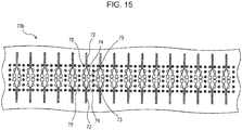
- FIG. 14 and FIG. 15 is a diagram illustrating an example mother board on which the AC coupling capacitor may be provided.
- a mother board 70a illustrated in FIG. 14 includes a structural portion which is provided in the middle of a single signal wire 72 through which a signal is transmitted, where the structural portion includes a pair of pad electrode portions 73 on which an AC coupling capacitor is to be mounted.
- Each of the signal wires 72 of the structural portion is provided within the mother board 70a and is extended to a signal electrode 74 provided on a surface of the mother board 70a through a via (not illustrated) to be electrically connected to the pad electrode portions 73.
- Ground electrodes 75 are disposed on the surface of the mother board 70a such that the signal electrode 74 connected to the pair of pad electrode portions 73 is interposed therebetween.
- the mother board 70a has a configuration in which a pair of the above-described structural portions is assumed as one group and a plurality of the groups are arranged.
- the mother board 70a including the above-described configuration, similar to the case illustrated in FIG. 3 , there is a probability that crosstalk occurs on the surface of the mother board 70a because the pad electrode portions 73 and the signal electrode 74 connected to one of different pairs of signal wires 72 are located adjacent to the pad electrode portions 73 and the signal electrode 74 connected the other one of the different pairs of signal wires 72.
- the ground electrodes 75 are disposed between the pad electrode portions 73 and the signal electrode 74 which are connected to one of different pairs of signal wires 72 and the pad electrode portions 73 and the signal electrode 74 which are connected to the other one of the different pairs of signal wires 72.
- the mother board 70b having the above-described electrode arrangement there is a probability that an area on which the AC coupling capacitor is mounted is increased and the overall size of the mother board 70b and the wire length are increased, thus resulting in increase in transmission loss.
- FIG. 16 is a diagram illustrating a sixth electrode arrangement example. Specifically, FIG. 16 is a schematic view of an example electrode arrangement in an area of a circuit board.
- the circuit board 10 illustrated in FIG. 16 includes, on a part of the surface 11, four ground electrode 21 disposed at vertexes of a rectangular area 20A and a pair of signal electrodes 22 disposed in the rectangular area 20A (indicated by dashed lines) and surrounded by the ground electrodes 21.
- the pair of signal electrodes 22 is arranged in the direction S.
- a pad electrode portion 22a disposed on the rectangular area 20A of the surface 11 is electrically coupled to the corresponding one of the signal electrodes 22.
- the circuit board 10 illustrated in FIG. 16 further includes a pair of electrode terminals 25 disposed within on the rectangular area 20A of the surface 11 so as to be arranged in the direction T.
- the pair of electrode terminals 25 is arranged on a line passing in an intermediate point between the pair of signal electrodes 22 and extending in a perpendicular direction to the direction S (that is, on a line extending in the direction T) .
- the interval between the pair of electrode terminals 25 is the same interval as or substantially the same interval as the interval a between the pair of signal electrodes 22.
- a pad electrode portion 25a disposed on the rectangular area 20A of the surface 11 is electrically coupled to the corresponding one of the electrode terminals 25.
- the electrode terminals 25 and the pad electrode portion 25a are arranged on the surface 11 of the circuit board 10 such that each of the electrode terminals 25 as a single body and the pad electrode portion 25a as a single body coupled thereto are electrically independent.
- Each of AC coupling capacitors 26 is connected to the pad electrode portion 22a coupled to the corresponding one of the signal electrodes 22 and the pad electrode portion 25a coupled to the corresponding one of the electrode terminals 25 of the circuit board 10 illustrated in FIG. 16 .
- the pad electrode portion 22a and the pad electrode portion 25a are connected to each other via the AC coupling capacitor 26.
- FIG. 17 is a diagram illustrating an example joint part where a circuit board and a component are connected together. Specifically, FIG. 17 is a perspective view schematically illustrating an example joint part where a circuit board and a mother board are connected.
- each of vias 15 provided in the circuit board 10 is coupled to the corresponding one of the ground electrodes 21 and the signal electrodes 22.
- a pair of signal wires 16 provided in the circuit board 10 is coupled to the vias 15 coupled to the pair of signal electrodes 22.
- Each of the AC coupling capacitors 26 is connected to the corresponding one of the pad electrode portions 22a coupled to the corresponding one of the signal electrodes 22 and the corresponding one of the pad electrode portion 25a coupled to the corresponding one of the electrode terminals 25.
- Each of the electrode terminals 25 is connected to the corresponding one of signal electrodes 62 provided on a surface of the mother board via the corresponding one of bumps 60.
- each of the ground electrodes 21 is connected to the corresponding one of ground electrodes 61 provided on the surface of the mother board via the corresponding one of the bumps 60.
- Each of vias 63 provided in the mother board is coupled to the corresponding one of the ground electrodes 61 and the signal electrodes 62.
- Signal wires 64 provided in the mother board are coupled to the vias 63 electrically connected to the electrode terminals 25.
- each of the signal electrodes 22 electrically coupled to the corresponding one of the signal wires 16 via the corresponding one of the vias 15 is electrically coupled to the corresponding one of the electrode terminals 25 via the corresponding one of the pad electrode portion 22a, the corresponding one of the AC coupling capacitors 26 and the corresponding one of the pad electrode portions 25a.
- Each of the electrode terminals 25 is electrically coupled to the corresponding one of the signal electrodes 62 of the mother board via the corresponding one of the bumps 60
- each of the signal electrodes 62 is electrically coupled to the corresponding one of the signal wires 64 via the corresponding one of the vias 63.
- the transmission paths extending from the signal electrodes 22 to the electrode terminals 25 on the surface 11 of the circuit board 10 are surrounded by the ground electrodes 21, the joint parts where the electrode terminals 25 and the signal electrodes 62 of the mother board are connected together are surrounded by the joint parts where the ground electrodes 21 of the circuit board 10 and the ground electrodes 61 of the mother board are connected together.
- crosstalk is reduced in an area between the circuit board 10 and the mother board.
- a larger space is allowed between the pair of signal electrodes 22 arranged in the direction S and the pair of ground electrodes 21 arranged in parallel to the pair of signal electrodes 22.
- the space is used as an arrangement area for the AC coupling capacitor 26.
- the space has a sufficient area for disposing the AC coupling capacitor 26 having a size which has a width of 0.3 mm, a length of 0.5 mm, and a thickness of 0.2 mm.
- the electrode terminals 25 function as electrodes used for connecting the circuit board 10 to the mother board using the bumps 60, and thus, it is preferable that the electrode terminals 25 have the same plane size or substantially the same plane size as the plane size of the ground electrodes 21.
- Use of the bumps 60 with the same or similar size in the plane size for both the electrode terminals 25 and the ground electrodes 21 may allow the circuit board 10 and the mother board to be connected together with a certain gap therebetween and connection failure between the circuit board 10 and the mother board may be reduced.
- the signal electrodes 22 function as electrodes electrically coupled to the pad electrode portion 22a to which the AC coupling capacitor 26 is connected, and therefore, the signal electrodes 22 may be formed so as to have a plane size having a diameter equal to or greater than a diameter (for example, 100 ⁇ m) of the vias 15 which connect the signal electrodes 22 to the signal wires 16.
- the circuit board 10 which is to be connected to the mother board may be formed in a structure in which the electrode terminals 25 are disposed in positions of the signal electrodes 22 in FIG. 6 when the AC coupling capacitors 26 are not mounted.
- the direction in which the signal electrodes 22 are arranged is a direction rotated by 90 degrees from the direction in which the signal electrodes 22 of FIG. 6 are arranged, and the signal wires 16 are electrically connected to the signal electrodes 22 thus provided.
- the circuit board 10 is formed to have the configuration of FIG. 17 , and thus, the electrode terminals 25 may be connected to the ground electrodes 61 using the bumps 60 without changing the structure of the mother board.
- FIG. 16 and FIG. 17 may be provided in each of a plurality of parts of the circuit board 10 such that multiple ones of the electrode arrangement are arranged so as to be adjacent to one another in accordance with the examples of FIGs. 7-10 .
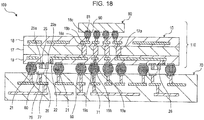
- FIG. 18 is a diagram illustrating an example electronic device using the above-described circuit board 10. Specifically, FIG. 18 is a cross-sectional view schematically illustrating an example of an electronic device, and for the sake of convenience, a part of electronic device illustrated in a perspective manner.
- An electronic device 100 illustrated in FIG. 18 includes a circuit board 10, a semiconductor element 80 mounted on the circuit board 10, and a mother board 70 connected to the circuit board 10 on which the semiconductor element 80 is mounted.
- FIG. 18 illustrates a case, as an example, where the electronic device 100 includes an AC coupling capacitor 26 mounted on a joint surface of the circuit board 10 and the joint surface is coupled to the mother board 70.
- the circuit board 10 is, for example, a build-up substrate including a core layer 17, and a wire layer 18 and a wire layer 19 provided on both sides of the core layer 17, respectively.
- Through hole vias 17a are provided in the core layer 17.
- Vias 18a and wires 18b electrically coupled to the through hole vias 17a are provided in the wire layer 18, and electrodes 18c are provided in positions corresponding to electrodes 81 of the semiconductor element 80 on a surface of the wire layer 18.
- the electrodes 18c of the circuit board 10 are connected to the electrodes 81 of the semiconductor element 80 via bumps 90, and thus, a semiconductor package 110 is formed in which the semiconductor element 80 is mounted on the circuit board 10.
- Vias 19a and wires 19b electrically coupled to the through hole vias 17a are provided in the wire layer 19, and electrodes 19c (30) are provided in positions corresponding to electrodes 71 of the mother board 70 on a central part of a surface of the wire layer 19 which faces to the mother board 70.
- the ground electrodes 21, the signal electrodes 22, and the electrode terminals 25 are provided on a peripheral part of the surface of the wire layer 19 which faces the mother board 70.
- Each of vias 19a (15) provided in the circuit board 10 is connected to the corresponding one of the ground electrodes 21 and the signal electrodes 22, and a wire 19b provided in the circuit board 10 to serve as a signal wire (16) is connected to the via 19a connected to the signal electrode 22.
- the AC coupling capacitor 26 which couples the corresponding one of the pad electrode portions 22a electrically connected to the corresponding one of the signal electrodes 22 and the corresponding one of the pad electrode portions 25a electrically connected to the corresponding one of the electrode terminals 25 is provided on the wire layer 19.
- the electrode terminals 25 are connected to the electrodes 71 provided on the surface of the mother board 70 via the bumps 60 (indicated by dashed lines) where the electrodes 71 serve as signal electrodes (62).
- the ground electrodes 21 are connected to the electrodes 71 provided on the surface of the mother board 70 via the bumps 60 where the electrodes 71 serve as ground electrodes (61).
- Vias 76 and wires 77 provided in the mother board 70 are coupled to the electrodes 71.
- the wires 77 provided in the mother board 70 to serve as signal wires (64) are coupled to the vias 76 electrically coupled to the electrode terminals 25.
- the electrodes 19c, the electrode terminals 25, and the ground electrodes 21 of the circuit board 10 on which the semiconductor element 80 is mounted are connected to the electrodes 71 of the mother board 70 via the bumps 60, and thus, the electronic device 100 in which the semiconductor package 110 is mounted on the mother board 70 is formed.
- the electronic device 100 which includes a transmission path for high frequency transmission in which low frequency noise may be cut or decreased by using the circuit board 10 including the AC coupling capacitors 26 provided on the circuit board 10.
- the electrode arrangement illustrated in FIG. 16 and FIG. 17 is employed for the circuit board 10, and thereby, crosstalk in the joint parts where the signal electrodes 22 and the electrodes 71 (the signal electrodes 62) are connected together via the bumps 60 may be reduced.
- the overall size of the circuit board 10 may be reduced, and the length of each wire may be reduced, and thus, transmission loss which occurs when a relatively high frequency signal is transmitted may be reduced.
- the above-described circuit board 10 is formed by stacking, on both surfaces of the core layer 17, the certain number of layers of sheet members on which a certain conductor pattern is formed.
- a substrate such as a glass epoxy substrate and the like, having a certain stiffness is used for the core layer 17, hole opening processing using a laser or the like is performed thereon to form holes in the substrate, and conductive parts are formed in the holes, thereby forming the through hole vias 17a.
- resin sheets made of epoxy resin or the like, having a certain flexibility, on which a certain conductor pattern is provided may be used.
- the certain number of layers of such sheet members are stacked, and thereby, the vias 18a and 19a, the wires 18b and 19b, and the electrodes 18c and electrodes 19c, as well as the ground electrodes 21, the signal electrodes 22, the electrode terminals 25, and the pad electrode portions 22a and 25a, are formed.
- a laminated body of prepreg with a conductor pattern provided on both of front and back surfaces thereof, or the front surface or the back surface thereof may be used.
- hole opening processing using a laser or the like may be performed on the certain number of layers of prepreg or a laminated body of prepreg and a conductive film may be formed in holes thus formed, thereby forming through holes which provide electrical conduction between the front and back surfaces.
- the semiconductor package 110 in which the semiconductor element 80 is mounted on the circuit board 10 has been described as an example in this embodiment, but another component (for example, a chip component, such as an AC coupling capacitor and the like), in addition to the semiconductor element 80, may be mounted on the circuit board 10.
- a chip component such as an AC coupling capacitor and the like
- a so-called component built-in type circuit board that is, a circuit board on which one of the above-described electrode arrangement is provided at least on a joint surface thereof with the mother board 70 and which includes a component, such as a semiconductor element and the like, provided therein, may be mounded on the mother board 70.
Description
- The embodiment discussed herein is related to a circuit board and an electronic device.
- Circuit boards on which various components are mounted have been widely used for electronic devices. For example, it has been known that an electronic device (a semiconductor package) includes a circuit board (a package substrate) on which a semiconductor element is mounted, or an electronic device includes a circuit board, such as a mother board, on which a semiconductor package is mounted. As the operation speed of electronic devices has increased, a differential transmission type circuit board as a circuit board has been used, signals in the differential transmission type circuit are transmitted through a pair of transmission paths.
- Japanese Laid-open Patent Publication No.
2001-203470 2010-192767 US 2012/0247825 discloses a printed circuit board including a top signal layer, a bottom signal layer, a ground layer, a plurality of vias and at least two ground vias. - In a circuit board which transmits signals in the circuit board or to outside the circuit board using a pair of transmission paths (wires in the circuit board and signal electrodes provided on a surface of the circuit board so as to be electrically connected to the wires and joined to another component), crosstalk between transmission paths of a different pair might be a problem.
- Accordingly, it is an object in one aspect of the invention to provide a circuit board in which excellent crosstalk reduction may be achieved in the circuit board and in a joint part where the signal electrode and an electrode of a component are joined.
- According to an aspect of the invention, there is proved a circuit board as defined in claim 1. Preferred features are defined in the dependent claims.
-
-
FIG. 1 is a diagram illustrating an example electronic device not forming part of the invention; -
FIGs. 2A-2B are (first) diagrams illustrating an example circuit board not forming part of the invention; -
FIG. 3 is a (second) diagram illustrating an example circuit board not forming part of the invention; -
FIG. 4 is a (third) diagram illustrating an example circuit board not forming part of the invention; -
FIG. 5 is a diagram illustrating a first electrode arrangement not forming part of the invention; -
FIG. 6 is a (first) diagram illustrating an example joint part not forming part of the invention, where a circuit board and a component are joined together; -
FIG. 7 is a diagram illustrating a second electrode arrangement not forming part of the invention; -
FIG. 8 is a diagram illustrating a third electrode arrangement not forming part of the invention; -
FIG. 9 is a diagram illustrating a fourth electrode arrangement not forming part of the invention; -
FIG. 10 is a diagram illustrating a fifth electrode arrangement not forming part of the invention; -
FIG. 11 is a diagram illustrating a simulation of crosstalk; -
FIG. 12 is a (first) graph illustrating an example simulation result; -
FIG. 13 is a (second) graph illustrating an example simulation result; -
FIG. 14 is a (first) diagram illustrating an example mother board not forming part of the invention; -
FIG. 15 is a (second) diagram illustrating an example mother board not forming part of the invention; -
FIG. 16 is a diagram illustrating an embodiment of an electrode arrangement according to the invention; -
FIG. 17 is a (second) diagram illustrating an example joint part where a circuit board and a component are joined together; accordingly to the invention; and -
FIG. 18 is a diagram illustrating an example electronic device using a circuit board as defined in the invention. -
FIG. 1 is a diagram illustrating an example electronic device. Specifically,FIG. 1 is a cross-sectional view illustrating a major part of an example electronic device. Anelectronic device 100a illustrated inFIG. 1 includes a package substrate (a circuit board) 200, asemiconductor element 300 mounted on thepackage substrate 200, and a mother board (a circuit board) 400 connected to thepackage substrate 200 on which thesemiconductor element 300 is mounted. - The
package substrate 200 is, for example, a build-up circuit board, and includes acore layer 210, andwire layers core layer 210 using a build-up technology. - A through hole via 211 is provided in the
core layer 210 of thepackage substrate 200. Avia 221 and awire 222 are provided in awire layer 220 provided on one side of thecore layer 210 so as to be electrically connected to the through hole via 211 of thecore layer 210, and an electrode 223 is provided on a surface of thewire layer 220 so as to be located in a position corresponding to anelectrode 310 of thesemiconductor element 300. Avia 231 and awire 232 are provided in awire layer 230 provided on the other side of thecore layer 210 so as to be electrically connected to the through hole via 211 of thecore layer 210, and anelectrode 233 is provided on a surface of thewire layer 230 so as to be located in a position corresponding to anelectrode 410 of themother board 400. - The
semiconductor element 300 is mounted on thepackage substrate 200 configured in the above-described manner. Theelectrode 310 of thesemiconductor element 300 and the electrode 223 of thepackage substrate 200 are joined together via abump 320, and thus, thesemiconductor element 300 is mounted on thepackage substrate 200. Thus, thesemiconductor element 300 is mounted on thepackage substrate 200 to form asemiconductor package 110a. - The
electrode 233 of thepackage substrate 200 of thesemiconductor package 110a is connected to theelectrode 410 of themother board 400 via abump 120, and thus, thesemiconductor package 110a is mounted on themother board 400. For example, a laminated body ofprepreg 420 may be used as themother board 400, where the laminated body ofprepreg 420 includes aconductor pattern 420a provided on both of front and back surfaces thereof, or the front surface or the back surface thereof may. Performing a hole-forming process to the laminated body prepreg 420 to form a hole and forming a conductive film in the hole, a throughhole 430 is formed so that the front surface of themother board 400 is electrically connected to the back surface thereof. - When a relatively high frequency signal is transmitted in the
electronic device 100a, an alternating current (AC)coupling capacitor 500 is provided on a transmission path through which the relatively high frequency signal is transmitted.FIG. 1 illustrates as an example a case where anAC coupling capacitor 500 is bonded, via asolder 510, to a transmission path of themother board 400 through which the relatively high frequency signal is transmitted. - Incidentally, some of the electronic device may use a circuit board, in which transmits a relatively high frequency signal, including a pair of transmission paths (pair transmission paths) through which a signal is transmitted by a differential transmission method. In such a circuit board, there is a probability that crosstalk (an electromagnetic interference) occurs between different pairs of transmission paths. One of methods for reducing crosstalk is to provide an electromagnetic shielding structure using a conductor body at a ground potential between the different pairs of transmission paths in the circuit board. On the other hand, signal electrodes extended from the pair transmission paths are exposed on a surface of the circuit board, and therefore, crosstalk might occur in a joint part where the signal electrode and an electrode of a component joined to the circuit board are joined together.
-
FIGs. 2A-2B ,FIG. 3 , andFIG. 4 are diagrams illustrating an example circuit board.FIGs. 2A-2B illustrate, as an example circuit board, apackage substrate 600 on which a semiconductor element is mounted. On onesurface 610 of thepackage substrate 600 illustrated inFIG. 2A , amounting area 611 for a semiconductor element is provided. On theother surface 620 of thepackage substrate 620 illustrated inFIG. 2B , a group ofelectrodes 621 for electrically coupling thepackage substrate 600 to another component, for example, a mother board, is provided, where theelectrodes 621 are arranged in a latticed pattern in a certain area. - When the
package substrate 600 includes the pair transmission paths, the group ofelectrodes 621 arranged in the latticed pattern as illustrated inFIG. 2B includes signal electrodes extending from pairs of wires (pair wires) provided in thepackage substrate 600. For example, as illustrated inFIG. 3 , the group ofelectrodes 621 includes pairs ofsignal electrodes 621a (a single pair is surrounded by a dashed line inFIG. 3 ) andground electrodes 621b, and these electrodes are mixedly arranged in the latticed pattern on thesurface 620 of thepackage substrate 600. - As illustrated in
FIG. 3 , when different pairs ofsignal electrodes 621a are disposed so as to be adjacent to one another, crosstalk might occur in thesignal electrodes 621a or joint parts where thesignal electrodes 621a and electrodes of the mother board are joined together. In order to reduce such crosstalk, for example, as illustrated inFIG. 4 ,ground electrodes 621b are disposed between the different pairs ofsignal electrodes 621a (a single pair is surrounded by a dashed line inFIG. 4 ), and thus, a certain distance is ensured between the different pairs ofsignal electrodes 621a. - As a result, however, the number of groups of electrodes 621 (including the
signal electrodes 621a and theground electrodes 621b) arranged on thesurface 620 of thepackage substrate 600 is increased, and accordingly, an arrangement area of the group ofelectrodes 621 is increased. If the number of pins provided in the semiconductor element which is mounted on the electronic device is increased because of the demand for high performance, the number of the groups ofelectrodes 621 and the arrangement area thereof are increased for the purpose of reducing crosstalk, thus increasing the number of pins provided on thepackage substrate 600 and the size of thepackage substrate 600. - On the other hand, in view of increasing the operation speed, in order to reduce a transmission loss which increases as the frequency increases, the group of
electrodes 621 is provided with reduced intervals to increase arrangement density, thereby reducing increase in size of thepackage substrate 600 due to increase in the number of pins and also reducing a wire length. - In the electrode arrangement illustrated in
FIG. 3 , crosstalk is not effectively reduced, and furthermore, in the electrode arrangement illustrated inFIG. 4 , although a certain crosstalk reduction effect is achieved, there is a probability that the number of pins provided in thepackage substrate 600 and the size of thepackage substrate 600 are increased, the wire length is increased, and thus, transmission loss is increased. - In view of the foregoing, according to this disclosure, an electrode arrangement illustrated in
FIG. 5 is employed for a circuit board, such as a package substrate, and the like.FIG. 5 is a diagram illustrating a first example of electrode arrangement. Specifically,FIG. 5 is a schematic view of an example electrode arrangement in a part of an area of a circuit board. - A
circuit board 10 illustrated inFIG. 5 includes, in a part of thesurface 11, fourground electrodes 21 disposed at vertexes of arectangular area 20A indicated by dashed lines and a pair ofsignal electrodes 22 disposed in therectangular area 20A and surrounded by theground electrodes 21. - The
circuit board 10 is, for example, a package substrate. Examples of the package substrate include various types of substrate, such as, a build-up substrate, a ceramic substrate, a glass ceramic substrate, a coreless substrate, and the like. Asurface 11 of thecircuit board 10 on which theground electrodes 21 and thesignal electrodes 22 are disposed is, for example, a surface which is joined to another component, such as a mother board, and the like. Theground electrodes 21 are electrodes which have a potential serving as a ground potential of thecircuit board 10, and the pair ofsignal electrodes 22 is electrodes each of which is electrically connected to the corresponding one of pair wires provided in thecircuit board 10. - The pair of
signal electrodes 22 is arranged in a direction S which is parallel to aside 23 of therectangular area 20A with an interval a (with a distance (a pitch) a) between respective centers of the pair of signal electrodes 22). Therectangular area 20A has, for example, a square shape. The fourground electrodes 21 are disposed at the vertexes of therectangular area 20A having a square shape with intervals b (with a pitch b between respective centers of the adjacent ones of the ground electrodes 21) which are greater than the interval a between the pair ofsignal electrodes 22. The interval b between adjacent two of theground electrodes 21 is set, for example, to be the double (b = a x 2) of the interval a between thesignal electrodes 22. Specifically, assuming that the interval a between thesignal electrodes 22 is 1 mm, the interval b between adjacent two of theground electrodes 21 is 2 mm. - Thus, for the
circuit board 10 illustrated inFIG. 5 , an electrode arrangement is employed in which the pair ofsignal electrodes 22 disposed in line in the direction S is surrounded by the fourground electrodes 21 disposed at the vertexes of therectangular area 20A having a square shape. By disposing the electrodes in the electrode arrangement illustrated inFIG. 5 , an electromagnetic interference from the pair ofsignal electrodes 22 to the other signal electrodes or to the pair ofsignal electrodes 22 from the other signal electrodes, that is, crosstalk, is reduced by the surrounding fourground electrodes 21. -
FIG. 6 is a diagram illustrating an example joint part where a circuit board and a component are joined together. Specifically,FIG. 6 is a perspective view schematically illustrating an example joint part where a circuit board and a mother board are joined together. InFIG. 6 , the fourground electrodes 21 and the pair ofsignal electrodes 22 are provided on the surface of thecircuit board 10 in the basis of the electrode arrangement illustrated inFIG. 5 . Each ofvias 15 provided in thecircuit board 10 is coupled to the corresponding one of theground electrodes 21 and thesignal electrodes 22. A pair of signal wires (pair wires) 16 provided in thecircuit board 10 is connected to thevias 15 connected to the pair ofsignal electrodes 22. - Each of the
ground electrodes 21 and thesignal electrodes 22 configured in the above-described manner is joined to the corresponding one ofground electrodes 61 andsignal electrodes 62 provided on the surface of the mother board via the corresponding one ofbumps 60. Each of the vias 63 provided in the mother board is coupled to the corresponding one of theground electrodes 61 andsignal electrodes 62.Signal wires 64 provided in the mother board are coupled to thevias 63 electrically connected to thesignal electrodes 22. - The
circuit board 10 including the electrode arrangement illustrated inFIG. 5 is, for example, connected to the mother board in the manner illustrated inFIG. 6 . The joint parts where thesignal electrodes 22 of thecircuit board 10 and thesignal electrodes 62 of the mother board are connected together are surrounded by the joint parts where theground electrodes 21 of thecircuit board 10 and theground electrodes 61 of the mother board are joined together, thus reducing crosstalk in the joint parts where thesignal electrodes 22 and thesignal electrodes 62 are joined together. - The electrode arrangement illustrated in
FIG. 5 may be provided on a plurality of parts of thesurface 11 of thecircuit board 10. -
FIG. 7 is a diagram illustrating a second electrode arrangement example. Specifically,FIG. 7 is a schematic view of an example of an electrode arrangement in an area of a circuit board. -
FIG. 7 illustrates, as an example, thecircuit board 10 on which the above-described electrode arrangement illustrated inFIG. 5 is provided on two adjacent parts of thesurface 11. - The
circuit board 10 illustrated inFIG. 7 includes, in thesurface 11, theground electrodes 21 disposed at the vertexes of therectangular area 20A and the pair ofsignal electrodes 22 disposed in therectangular area 20A so as to be arranged in the direction S. - Furthermore, the
circuit board 10 illustrated inFIG. 7 includes, in thesurface 11, fourground electrodes 21 disposed at vertexes of arectangular area 20B located adjacent to therectangular area 20A and a pair ofsignal electrodes 22 disposed in therectangular area 20B. The pair ofsignal electrodes 22 disposed in therectangular area 20B is arranged in a direction T which is parallel to aside 24 of therectangular area 20B and is perpendicular to the direction S. - In the example of
FIG. 7 , on the boundary of therectangular area 20A and therectangular area 20B, the pair ofground electrodes 21 disposed in therectangular area 20A so as to be arranged in the direction T and the pair ofground electrodes 21 disposed in therectangular area 20B so as to be arranged in the direction T are common. - As illustrated in
FIG. 7 , the two pairs ofsignal electrodes 22 are arranged in the direction S and the direction T which are perpendicular to each other, and thus, as compared to the case where the two pairs are arranged in the same direction, the two pairs ofsignal electrodes 22 may be disposed with an increased distance between the two pairs. - Also, when the electrode arrangement of the latticed pattern illustrated in
FIG. 4 is employed for the two pairs ofsignal electrodes 22, sixteenground electrodes 21 are provided in order to reduce crosstalk. In contrast, in the electrode arrangement ofFIG. 7 , only sixground electrodes 21 are enough to reduce crosstalk. That is, using the electrode arrangement illustrated inFIG. 7 , reduction in number of electrodes disposed on thesurface 11 of thecircuit board 10 is achieved. -
FIG. 8 is an explanatory diagram illustrating a third electrode arrangement example. Specifically,FIG. 8 is a schematic view of an example electrode arrangement in an area of a circuit board.FIG. 8 illustrates, as an example, thecircuit board 10 on which multiple ones of the electrode arrangement illustrated inFIG. 7 are provided in combination on thesurface 11 such that some of the pairs ofground electrodes 21 are shared. On thecircuit board 10 ofFIG. 8 , theground electrodes 21 and thesignal electrodes 22 are disposed such that each of the directions (the directions U and V indicated by dashed lines inFIG. 8 ) in which the pairs of thesignal electrodes 22 are arranged is a direction which is neither parallel to anend side 12 of thecircuit board 10 nor perpendicular to theend side 12. That is, theground electrodes 21 and thesignal electrodes 22 are disposed on thecircuit board 10 such that each of the directions U and V in which the pairs of thesignal electrodes 22 are arranged intersects theend side 12 at an acute angle of θ. For example, theground electrodes 21 and thesignal electrodes 22 are arranged such that the directions U and V in which the pairs of thesignal electrodes 22 are arranged form an equal angle θ, that is, 45 degrees, with theend side 12 of thecircuit board 10. - By arranging the
ground electrodes 21 and thesignal electrodes 22 as illustrated inFIG. 8 , as compared to the electrode arrangement of the latticed pattern illustrated inFIG. 4 , it may be achieved to reduce the number ofground electrodes 21 disposed in order to surround a certain number of pairs ofsignal electrodes 22. - Furthermore, by arranging the
ground electrodes 21 and thesignal electrodes 22 as illustrated inFIG. 8 , it may be achieved to reduce the length of an arrangement area for theground electrodes 21 and thesignal electrodes 22. For example,FIG. 8 illustrates a case where seven pairs ofsignal electrodes 22 are arranged. In this case, the length L of an electrode arrangement area may be reduced by about 20%, as compared to the case where seven pairs ofsignal electrodes 621a are arranged as illustrated inFIG. 4 . -
FIG. 9 is an explanatory diagram illustrating a fourth electrode arrangement example. Specifically,FIG. 9 is a schematic plan view of a circuit board viewed from one surface side of the circuit board.FIG. 9 illustrates, as an example, thecircuit board 10 on which a plurality of electrodes according to the electrode arrangement illustrated inFIG. 8 is provided in aperipheral part 13 of thesurface 11. A group ofelectrodes 30 is arranged in a latticed pattern in a further inner area than theperipheral part 13 in thecircuit board 10. - By arranging pairs of
signal electrodes 22 in theperipheral part 13 as in thecircuit board 10 illustrated inFIG. 9 , it may be reduced to occur a worse situation where wires extended from the pairs ofsignal electrodes 22 are located close to other electrodes (signal electrodes) , and thus, crosstalk may be reduced. - By forming the
peripheral part 13 of thecircuit board 10 in the electrode arrangement illustrated inFIG. 9 , the number ofground electrodes 21 surrounding a certain number of pairs ofsignal electrodes 22 may be reduced, as compared to the case (FIG. 4 ) where thesignal electrodes 22 and theground electrodes 21 are arranged in a latticed pattern. - Furthermore, by forming the
peripheral part 13 of thecircuit board 10 in the electrode arrangement illustrated inFIG. 9 , when a certain number of pairs ofsignal electrodes 22 are provided in theperipheral part 13, the length of the electrode arrangement area may be reduced, as compared to the case (FIG. 4 ) where the pairs ofsignal electrodes 22 are arranged in a latticed pattern with theground electrodes 21. - Using the
circuit board 10 illustrated inFIG. 9 , it may be achieved to reduce crosstalk in the joint parts where thecircuit board 10 and the mother board are joined together via thesignal electrodes 22 by the reduced number of theground electrodes 21 provided around thesignal electrodes 22. Furthermore, it may be achieved to reduce the length of the arrangement area in theperipheral part 13 in which theground electrodes 21 and thesignal electrodes 22 are arranged. Accordingly, the overall size of thecircuit board 10 may be reduced. The reduction in overall size of thecircuit board 10 enables reduction in length of wires extended from thesignal electrodes 22, and thus, when thecircuit board 10 is used in transmitting a relatively high frequency signal, transmission loss may be reduced. - In the
circuit board 10 which includes, in theperipheral part 13, pairs of thesignal electrodes 22 and theground electrodes 21 surrounding them as illustrated inFIG. 9 , power supply electrodes (electrodes having a power supply potential or a ground potential) are disposed aselectrodes 30 in a further inner area than theperipheral part 13. - Note that, when electrodes for use in transmitting a relatively high frequency signal and electrodes for a relatively low frequency signal are arranged in the
circuit board 10, the electrodes for use in transmitting a relatively high frequency signal are disposed as thesignal electrodes 22 in theperipheral part 13 and the electrodes for use in transmitting relatively low frequency signals are disposed as theelectrodes 30 in a further inner side than theperipheral part 13. As described above, a group of theelectrodes 30 located in a central part of thecircuit board 10 may include, in addition to the power supply electrode, signal electrodes for use in transmitting signals. - The
electrodes 30 may be arranged in a latticed pattern, as illustrated inFIG. 9 . In this case, theelectrodes 30 are arranged in a latticed pattern with the same intervals as or substantially the same intervals as the interval a between a pair ofsignal electrodes 22 arranged in theperipheral part 13. By forming the electrode arrangement located in the central part of thecircuit board 10 into a lattice pattern, theelectrodes 30 may be arranged with higher density in the central part, as compared to the electrode arrangement in theperipheral part 13. By arranging theelectrodes 30 in this way, diminution in the total number of electrodes provided on thecircuit board 10 may be prevented. - Note that, although
FIG. 9 explanatory illustrates a configuration of a non-electrode formation area, in the central part of thesurface 11 of thecircuit board 10, without forming the group ofelectrodes 30, thecircuit board 10 may be configured such that theelectrodes 30 are arranged in a latticed pattern in the central part of thesurface 11. - In the above description, using the
surface 11 of thecircuit board 10 which is joined to the mother board as an example, it has been described to arrange theground electrodes 21 and thesignal electrodes 22, and theelectrodes 30. The above-described electrode arrangement illustrated inFIG. 8 may be employed for a surface of thecircuit board 10 to which a semiconductor element is joined (mounted). -
FIG. 10 is a diagram illustrating a fifth electrode arrangement example. Specifically,FIG. 10 is a schematic plan view of a circuit board viewed from the other surface side of the circuit board. -
FIG. 10 illustrates as an example a configuration in which the above-described electrode arrangement illustrated inFIG. 8 is employed for a semiconductorelement mounting area 14a provided in asurface 14 of thecircuit board 10 on which a semiconductor element is mounted. - Similar to
FIG. 8 , for the mountingarea 14a, multiple ones of an electrode arrangement in which a pair ofsignal electrodes 22 is surrounded by fourground electrodes 21 disposed at vertexes of a rectangular area are provided in combination in a peripheral part 14aa such that some of the pairs ofground electrodes 21 are shared. Adjacent pairs ofsignal electrodes 22 are arranged such that the direction in which one of the adjacent pairs ofsignal electrodes 22 is perpendicular to the direction in which the other one of the adjacent pairs. The pairs ofsignal electrodes 22 are disposed in the mountingarea 14a such that the direction in which each pair is arranged forms an equal angle (45 degrees) with an end side 14ab of the mountingarea 14a. - Power supply electrodes and signal electrodes for use in transmitting relatively low frequency signals may be provided in a further inner area than the peripheral part 14aa in the mounting
area 14a so as to be arranged in a latticed pattern. - By employing the electrode arrangement illustrated in
FIG. 10 for the semiconductorelement mounting area 14a, the number of theground electrodes 21 provided around thesignal electrodes 22 may be reduced, thus, enabling reduction of crosstalk in the joint parts where thecircuit board 10 and the semiconductor element are joined together via thesignal electrodes 22. Furthermore, by using the electrode arrangement illustrated inFIG. 10 , the size of the mountingarea 14a may be reduced, and the length of each wire provided in thecircuit board 10 may be reduced. - Subsequently, simulations of possible crosstalk which might occur when the above-described electrode arrangements are employed will be described.
-
FIG. 11 is a diagram illustrating a simulation of crosstalk, andFIG. 12 andFIG. 13 are graphs illustrating example simulation results. - In the simulation, as illustrated in
FIG. 11 , assuming that a transmission path between a port 1 and aport 2 is areference transmission path 5 and a transmission path between aport 3 and aport 4 is an evaluationtarget transmission path 6, crosstalk which the evaluationtarget transmission path 6 receives from thereference transmission path 5 is evaluated. Thetransmission path 5 and thetransmission path 6 are joint parts (joint parts of different pairs) where the signal electrodes 22 (which correspond to the port 1 and port 3) of thecircuit board 10 and electrodes (which correspond to theport 2 and the port 4) of a component, such as a mother board, are joined together. In the simulation, as crosstalk, a near-end crosstalk (Sdd31) between the port 1 and theport 3 and a far-end crosstalk (Sdd41) between the port 1 and theport 4 are evaluated. -
FIG. 12 andFIG. 13 illustrate an example of the relationship between a transmission signal frequency [GHz] obtained by the simulation and the near-end crosstalk Sdd31 [dB] and an example of the relationship between the transmission signal frequency [GHz] and the far-end crosstalk Sdd41 [dB], respectively. Each ofFIG. 12 andFIG. 13 indicates a result X obtained when the electrode arrangement ofFIG. 3 was employed for thetransmission path 5 and thetransmission path 6, a result Y obtained when the electrode arrangement ofFIG. 4 was employed for thetransmission path 5 and thetransmission path 6, and a result Z obtained when the electrode arrangement ofFIG. 8 was employed for thetransmission path 5 and thetransmission path 6. - It is understood from
FIG. 12 andFIG. 13 that the near-end crosstalk Sdd31 and the far-end crosstalk Sdd41 may be reduced by employing the electrode arrangement ofFIG. 4 for the electrode arrangement ofFIG. 3 (the result X and Y). It is also understood fromFIG. 12 andFIG. 13 that, when the electrode arrangement ofFIG. 8 is employed, the near-end crosstalk Sdd31 and the far-end crosstalk Sdd41 may be further reduced, as compared those when the electrode arrangement ofFIG. 4 is employed (the result Y and Z). - Using the electrode arrangement of
FIG. 8 , in addition to the above-described advantages, such as reduction in the number of theground electrodes 21, reduction in the length of an electrode arrangement area, and the like, an excellent crosstalk reduction effect may be advantageously achieved. Thecircuit board 10 including an electrode arrangement which enables reduction of crosstalk in joint parts where thecircuit board 10 and a component, such as a mother board and a semiconductor element has been described above. In an electronic device including a transmission path through which a relatively high frequency signal is transmitted using thecircuit board 10, there are cases where, in order to cut low frequency noise, an AC coupling capacitor is provided on such a transmission path through which a high frequency signal is transmitted. The AC coupling capacitor may be mounted not only on thecircuit board 10 but also on a mother board joined to thecircuit board 10, as long as the AC coupling capacitor is provided on a transmission path through which a high frequency signal is transmitted in the electronic device. - Each of
FIG. 14 andFIG. 15 is a diagram illustrating an example mother board on which the AC coupling capacitor may be provided. Amother board 70a illustrated inFIG. 14 includes a structural portion which is provided in the middle of asingle signal wire 72 through which a signal is transmitted, where the structural portion includes a pair ofpad electrode portions 73 on which an AC coupling capacitor is to be mounted. Each of thesignal wires 72 of the structural portion is provided within themother board 70a and is extended to asignal electrode 74 provided on a surface of themother board 70a through a via (not illustrated) to be electrically connected to thepad electrode portions 73.Ground electrodes 75 are disposed on the surface of themother board 70a such that thesignal electrode 74 connected to the pair ofpad electrode portions 73 is interposed therebetween. Themother board 70a has a configuration in which a pair of the above-described structural portions is assumed as one group and a plurality of the groups are arranged. - In the
mother board 70a including the above-described configuration, similar to the case illustrated inFIG. 3 , there is a probability that crosstalk occurs on the surface of themother board 70a because thepad electrode portions 73 and thesignal electrode 74 connected to one of different pairs ofsignal wires 72 are located adjacent to thepad electrode portions 73 and thesignal electrode 74 connected the other one of the different pairs ofsignal wires 72. - In order to reduce such crosstalk, on the basis of the same view as that applied to the case of
FIG. 4 , in amother board 70b illustrated inFIG. 15 , theground electrodes 75 are disposed between thepad electrode portions 73 and thesignal electrode 74 which are connected to one of different pairs ofsignal wires 72 and thepad electrode portions 73 and thesignal electrode 74 which are connected to the other one of the different pairs ofsignal wires 72. However, in themother board 70b having the above-described electrode arrangement, there is a probability that an area on which the AC coupling capacitor is mounted is increased and the overall size of themother board 70b and the wire length are increased, thus resulting in increase in transmission loss. - In view of the foregoing, an example method for mounting an AC coupling capacitor on the
circuit board 10 will be described.FIG. 16 is a diagram illustrating a sixth electrode arrangement example. Specifically,FIG. 16 is a schematic view of an example electrode arrangement in an area of a circuit board. - Similar to
FIG. 5 , thecircuit board 10 illustrated inFIG. 16 includes, on a part of thesurface 11, fourground electrode 21 disposed at vertexes of arectangular area 20A and a pair ofsignal electrodes 22 disposed in therectangular area 20A (indicated by dashed lines) and surrounded by theground electrodes 21. The pair ofsignal electrodes 22 is arranged in the direction S. Apad electrode portion 22a disposed on therectangular area 20A of thesurface 11 is electrically coupled to the corresponding one of thesignal electrodes 22. - The
circuit board 10 illustrated inFIG. 16 further includes a pair ofelectrode terminals 25 disposed within on therectangular area 20A of thesurface 11 so as to be arranged in the direction T. For example, the pair ofelectrode terminals 25 is arranged on a line passing in an intermediate point between the pair ofsignal electrodes 22 and extending in a perpendicular direction to the direction S (that is, on a line extending in the direction T) . The interval between the pair ofelectrode terminals 25 is the same interval as or substantially the same interval as the interval a between the pair ofsignal electrodes 22. Apad electrode portion 25a disposed on therectangular area 20A of thesurface 11 is electrically coupled to the corresponding one of theelectrode terminals 25. Theelectrode terminals 25 and thepad electrode portion 25a are arranged on thesurface 11 of thecircuit board 10 such that each of theelectrode terminals 25 as a single body and thepad electrode portion 25a as a single body coupled thereto are electrically independent. - Each of
AC coupling capacitors 26 is connected to thepad electrode portion 22a coupled to the corresponding one of thesignal electrodes 22 and thepad electrode portion 25a coupled to the corresponding one of theelectrode terminals 25 of thecircuit board 10 illustrated inFIG. 16 . Thus, thepad electrode portion 22a and thepad electrode portion 25a are connected to each other via theAC coupling capacitor 26. - The
circuit board 10 including the configuration illustrated inFIG. 16 is connected to a component, such as a mother board and the like.FIG. 17 is a diagram illustrating an example joint part where a circuit board and a component are connected together. Specifically,FIG. 17 is a perspective view schematically illustrating an example joint part where a circuit board and a mother board are connected. - In
FIG. 17 , fourground electrodes 21 and a pair ofsignal electrodes 22 are provided on a surface of thecircuit board 10 in the above-described electrode arrangement illustrated inFIG. 16 . Each ofvias 15 provided in thecircuit board 10 is coupled to the corresponding one of theground electrodes 21 and thesignal electrodes 22. A pair ofsignal wires 16 provided in thecircuit board 10 is coupled to thevias 15 coupled to the pair ofsignal electrodes 22. Each of theAC coupling capacitors 26 is connected to the corresponding one of thepad electrode portions 22a coupled to the corresponding one of thesignal electrodes 22 and the corresponding one of thepad electrode portion 25a coupled to the corresponding one of theelectrode terminals 25. - Each of the
electrode terminals 25 is connected to the corresponding one ofsignal electrodes 62 provided on a surface of the mother board via the corresponding one ofbumps 60. Similarly, each of theground electrodes 21 is connected to the corresponding one ofground electrodes 61 provided on the surface of the mother board via the corresponding one of thebumps 60. Each ofvias 63 provided in the mother board is coupled to the corresponding one of theground electrodes 61 and thesignal electrodes 62.Signal wires 64 provided in the mother board are coupled to thevias 63 electrically connected to theelectrode terminals 25. - As described above, in the example of
FIG. 17 , each of thesignal electrodes 22 electrically coupled to the corresponding one of thesignal wires 16 via the corresponding one of thevias 15 is electrically coupled to the corresponding one of theelectrode terminals 25 via the corresponding one of thepad electrode portion 22a, the corresponding one of theAC coupling capacitors 26 and the corresponding one of thepad electrode portions 25a. Each of theelectrode terminals 25 is electrically coupled to the corresponding one of thesignal electrodes 62 of the mother board via the corresponding one of thebumps 60, and each of thesignal electrodes 62 is electrically coupled to the corresponding one of thesignal wires 64 via the corresponding one of thevias 63. Thus, a transmission path including theAC coupling capacitor 26 in the middle of the transmission path may be achieved, and accordingly, a transmission path which suppresses low frequency noise and transmits a high frequency signal and an electronic device including the transmission path may be achieved. - The transmission paths extending from the
signal electrodes 22 to theelectrode terminals 25 on thesurface 11 of thecircuit board 10 are surrounded by theground electrodes 21, the joint parts where theelectrode terminals 25 and thesignal electrodes 62 of the mother board are connected together are surrounded by the joint parts where theground electrodes 21 of thecircuit board 10 and theground electrodes 61 of the mother board are connected together. Thus, crosstalk is reduced in an area between thecircuit board 10 and the mother board. - In the electrode arrangement illustrated in
FIG. 16 andFIG. 17 , as compared to an electrode arrangement including a simple lattice pattern, a larger space is allowed between the pair ofsignal electrodes 22 arranged in the direction S and the pair ofground electrodes 21 arranged in parallel to the pair ofsignal electrodes 22. The space is used as an arrangement area for theAC coupling capacitor 26. For example, when it is assumed that the interval a between thesignal electrodes 22 is 1 mm and the interval b between theground electrodes 21 is 2 mm, the space has a sufficient area for disposing theAC coupling capacitor 26 having a size which has a width of 0.3 mm, a length of 0.5 mm, and a thickness of 0.2 mm. - Similar to the
ground electrodes 21, theelectrode terminals 25 function as electrodes used for connecting thecircuit board 10 to the mother board using thebumps 60, and thus, it is preferable that theelectrode terminals 25 have the same plane size or substantially the same plane size as the plane size of theground electrodes 21. Use of thebumps 60 with the same or similar size in the plane size for both theelectrode terminals 25 and theground electrodes 21 may allow thecircuit board 10 and the mother board to be connected together with a certain gap therebetween and connection failure between thecircuit board 10 and the mother board may be reduced. Thesignal electrodes 22 function as electrodes electrically coupled to thepad electrode portion 22a to which theAC coupling capacitor 26 is connected, and therefore, thesignal electrodes 22 may be formed so as to have a plane size having a diameter equal to or greater than a diameter (for example, 100 µm) of the vias 15 which connect thesignal electrodes 22 to thesignal wires 16. - Also, as illustrated in
FIG. 17 , thecircuit board 10 which is to be connected to the mother board may be formed in a structure in which theelectrode terminals 25 are disposed in positions of thesignal electrodes 22 inFIG. 6 when theAC coupling capacitors 26 are not mounted. In thecircuit board 10 ofFIG. 17 , the direction in which thesignal electrodes 22 are arranged is a direction rotated by 90 degrees from the direction in which thesignal electrodes 22 ofFIG. 6 are arranged, and thesignal wires 16 are electrically connected to thesignal electrodes 22 thus provided. Thecircuit board 10 is formed to have the configuration ofFIG. 17 , and thus, theelectrode terminals 25 may be connected to theground electrodes 61 using thebumps 60 without changing the structure of the mother board. - The electrode arrangement illustrated in
FIG. 16 andFIG. 17 may be provided in each of a plurality of parts of thecircuit board 10 such that multiple ones of the electrode arrangement are arranged so as to be adjacent to one another in accordance with the examples ofFIGs. 7-10 .FIG. 18 is a diagram illustrating an example electronic device using the above-describedcircuit board 10. Specifically,FIG. 18 is a cross-sectional view schematically illustrating an example of an electronic device, and for the sake of convenience, a part of electronic device illustrated in a perspective manner. - An
electronic device 100 illustrated inFIG. 18 includes acircuit board 10, asemiconductor element 80 mounted on thecircuit board 10, and amother board 70 connected to thecircuit board 10 on which thesemiconductor element 80 is mounted.FIG. 18 illustrates a case, as an example, where theelectronic device 100 includes anAC coupling capacitor 26 mounted on a joint surface of thecircuit board 10 and the joint surface is coupled to themother board 70. - The
circuit board 10 is, for example, a build-up substrate including acore layer 17, and awire layer 18 and awire layer 19 provided on both sides of thecore layer 17, respectively. Throughhole vias 17a are provided in thecore layer 17. - Vias 18a and
wires 18b electrically coupled to the throughhole vias 17a are provided in thewire layer 18, andelectrodes 18c are provided in positions corresponding toelectrodes 81 of thesemiconductor element 80 on a surface of thewire layer 18. Theelectrodes 18c of thecircuit board 10 are connected to theelectrodes 81 of thesemiconductor element 80 viabumps 90, and thus, asemiconductor package 110 is formed in which thesemiconductor element 80 is mounted on thecircuit board 10. - Vias 19a and
wires 19b electrically coupled to the throughhole vias 17a are provided in thewire layer 19, andelectrodes 19c (30) are provided in positions corresponding toelectrodes 71 of themother board 70 on a central part of a surface of thewire layer 19 which faces to themother board 70. - The
ground electrodes 21, thesignal electrodes 22, and theelectrode terminals 25 are provided on a peripheral part of the surface of thewire layer 19 which faces themother board 70. Each ofvias 19a (15) provided in thecircuit board 10 is connected to the corresponding one of theground electrodes 21 and thesignal electrodes 22, and awire 19b provided in thecircuit board 10 to serve as a signal wire (16) is connected to the via 19a connected to thesignal electrode 22. TheAC coupling capacitor 26 which couples the corresponding one of thepad electrode portions 22a electrically connected to the corresponding one of thesignal electrodes 22 and the corresponding one of thepad electrode portions 25a electrically connected to the corresponding one of theelectrode terminals 25 is provided on thewire layer 19. - The
electrode terminals 25 are connected to theelectrodes 71 provided on the surface of themother board 70 via the bumps 60 (indicated by dashed lines) where theelectrodes 71 serve as signal electrodes (62). Similarly, theground electrodes 21 are connected to theelectrodes 71 provided on the surface of themother board 70 via thebumps 60 where theelectrodes 71 serve as ground electrodes (61).Vias 76 andwires 77 provided in themother board 70 are coupled to theelectrodes 71. Thewires 77 provided in themother board 70 to serve as signal wires (64) are coupled to thevias 76 electrically coupled to theelectrode terminals 25. - The
electrodes 19c, theelectrode terminals 25, and theground electrodes 21 of thecircuit board 10 on which thesemiconductor element 80 is mounted are connected to theelectrodes 71 of themother board 70 via thebumps 60, and thus, theelectronic device 100 in which thesemiconductor package 110 is mounted on themother board 70 is formed. - Thus, the
electronic device 100 is achieved which includes a transmission path for high frequency transmission in which low frequency noise may be cut or decreased by using thecircuit board 10 including theAC coupling capacitors 26 provided on thecircuit board 10. In theelectronic device 100, the electrode arrangement illustrated inFIG. 16 andFIG. 17 is employed for thecircuit board 10, and thereby, crosstalk in the joint parts where thesignal electrodes 22 and the electrodes 71 (the signal electrodes 62) are connected together via thebumps 60 may be reduced. Furthermore, the overall size of thecircuit board 10 may be reduced, and the length of each wire may be reduced, and thus, transmission loss which occurs when a relatively high frequency signal is transmitted may be reduced. - Note that the above-described
circuit board 10 is formed by stacking, on both surfaces of thecore layer 17, the certain number of layers of sheet members on which a certain conductor pattern is formed. A substrate, such as a glass epoxy substrate and the like, having a certain stiffness is used for thecore layer 17, hole opening processing using a laser or the like is performed thereon to form holes in the substrate, and conductive parts are formed in the holes, thereby forming the throughhole vias 17a. For the sheet members stacked on thecore layer 17, for example, resin sheets made of epoxy resin or the like, having a certain flexibility, on which a certain conductor pattern is provided, may be used. The certain number of layers of such sheet members are stacked, and thereby, thevias wires electrodes 18c andelectrodes 19c, as well as theground electrodes 21, thesignal electrodes 22, theelectrode terminals 25, and thepad electrode portions - For the
mother board 70, for example, a laminated body of prepreg with a conductor pattern provided on both of front and back surfaces thereof, or the front surface or the back surface thereof may be used. For themother board 70, hole opening processing using a laser or the like may be performed on the certain number of layers of prepreg or a laminated body of prepreg and a conductive film may be formed in holes thus formed, thereby forming through holes which provide electrical conduction between the front and back surfaces. - Note that the
electronic device 100 in which theAC coupling capacitor 26 is provided on thecircuit board 10 has been described as an example in this embodiment, but a transmission path may be provided on themother board 70 and theAC coupling capacitor 26 may be provided on the transmission path. - Also, the
semiconductor package 110 in which thesemiconductor element 80 is mounted on thecircuit board 10 has been described as an example in this embodiment, but another component (for example, a chip component, such as an AC coupling capacitor and the like), in addition to thesemiconductor element 80, may be mounted on thecircuit board 10. - Furthermore, a so-called component built-in type circuit board, that is, a circuit board on which one of the above-described electrode arrangement is provided at least on a joint surface thereof with the
mother board 70 and which includes a component, such as a semiconductor element and the like, provided therein, may be mounded on themother board 70.
Claims (14)
- A circuit board (10) comprising:a substrate;a first ground electrode group that includes a plurality of first ground electrodes (21), each of the plurality of the first ground electrodes being disposed at a corresponding one of vertexes of a first rectangular area (20A) in a surface (11) of the substrate;a first pair of signal electrodes (22) disposed in the first rectangular area (20A), the pair of the signal electrodes being arranged in a first direction (S, U) parallel to a side (23) of the first rectangular area; characterized in that the circuit board (10) further comprisesa pair of electrode terminals (25) arranged in the first rectangular area (20A) of the surface (11), the pair of the electrode terminals being not electrically coupled to the first ground electrode group; andcapacitors (26) provided above the surface (11), one of the capacitors coupling one of the pair of the electrode terminals (25) and the corresponding one of the first pair of the signal electrodes (22).
- The circuit board (10) according to claim 1, further comprising
a second ground electrode group that includes a plurality of second ground electrodes (21), each of the plurality of the second ground electrodes being disposed at a corresponding one of vertexes of a second rectangular area (20B), the second rectangular area being adjacent to the first rectangular area (20A) in the surface (11); and
a second pair of signal electrodes (22) disposed in the second rectangular area (20B) of the surface, the second pair of the signal electrodes being arranged in a second direction (T, V) perpendicular to the first direction (S, U). - The circuit board (10) according to claim 2, wherein a first pair of the first ground electrodes (21) in the first ground electrode group and a second pair of the second ground electrodes (22) in the second ground electrode group are common.
- The circuit board (10) according to any of claims 1 to 3, wherein the first ground electrode group of the first ground electrodes (21) and the first pair of the signal electrodes (22) are arranged in a peripheral part (13) of the surface (11).
- The circuit board (10) according to claim 4, further comprising
a group of electrodes (30) arranged so as to be in a lattice pattern in a further inner area than the peripheral part (13) in the surface (11). - The circuit board (10) according to any of claims 1 to 4, further comprising
a pair of wires (16) that is provided in the substrate, a differential signal being transmitted to the pair of the wires,
wherein the first pair of the signal electrodes (22) are electrically coupled to the pair of the wires (16). - The circuit board according to claim 1, wherein the pair of the electrode terminals is arranged on a line passing in an intermediate point between the first pair of the signal electrodes and extending in a perpendicular direction to the first direction.
- An electronic device (100) including the circuit board (10) according to claim 1 as a first circuit board, further comprising
an electronic component (80) mounted on the first circuit board (10). - The electronic device according to claim 8, wherein the first circuit board (10) further includes,
a second ground electrode group that includes a plurality of second ground electrodes (21), each of the plurality of the second ground electrodes being disposed at a corresponding one of vertexes of a second rectangular area (20B), the second rectangular area being adjacent to the first rectangular area (20A) in the surface; and
a second pair of signal electrodes (21) disposed in the second rectangular area (20B) of the surface, the second pair of the signal electrodes (22) being arranged in a second direction (T, V) perpendicular to the first direction (S, U). - The electronic device (100) according to claim 8 or 9, wherein the first direction (U) is a direction intersecting an end side (12) of the substrate at an acute angle.
- The electronic device (100) according to any of claims 8 to 10, wherein the first ground electrode group of the ground electrodes (21) and the first pair of the signal electrodes (22) of the first circuit board (10) are arranged in a peripheral part (13) of the surface (11).
- The electronic device (100) according to claim 11, wherein the first circuit board (10) further includes,
a group of electrodes (30) arranged so as to be in a lattice pattern in a further inner area than the peripheral part (13) in the surface (11). - The electronic device (100) according to any of claims 8 to 12, further comprising a second circuit board (70) on which the first circuit board (10) is mounted.
- The electronic device (100) according to claim 13,
wherein each of the pair of electrode terminals is electrically coupled to the second circuit board (70).
Applications Claiming Priority (1)
| Application Number | Priority Date | Filing Date | Title |
|---|---|---|---|
| JP2013067954A JP6098285B2 (en) | 2013-03-28 | 2013-03-28 | Wiring board and electronic device |
Publications (3)
| Publication Number | Publication Date |
|---|---|
| EP2785155A2 EP2785155A2 (en) | 2014-10-01 |
| EP2785155A3 EP2785155A3 (en) | 2016-01-27 |
| EP2785155B1 true EP2785155B1 (en) | 2018-01-03 |
Family
ID=50280254
Family Applications (1)
| Application Number | Title | Priority Date | Filing Date |
|---|---|---|---|
| EP14160209.4A Not-in-force EP2785155B1 (en) | 2013-03-28 | 2014-03-17 | Circuit board and electronic device |
Country Status (3)
| Country | Link |
|---|---|
| US (1) | US9699887B2 (en) |
| EP (1) | EP2785155B1 (en) |
| JP (1) | JP6098285B2 (en) |
Families Citing this family (7)
| Publication number | Priority date | Publication date | Assignee | Title |
|---|---|---|---|---|
| JP6534312B2 (en) * | 2015-07-31 | 2019-06-26 | ルネサスエレクトロニクス株式会社 | Semiconductor device |
| US9848488B1 (en) * | 2016-06-17 | 2017-12-19 | Macom Technology Solutions Holdings, Inc. | Electrical interface for printed circuit board, package and die |
| US10314163B2 (en) * | 2017-05-17 | 2019-06-04 | Xilinx, Inc. | Low crosstalk vertical connection interface |
| JP6844035B2 (en) * | 2017-12-13 | 2021-03-17 | 株式会社日立製作所 | Wiring board and electronic equipment |
| US11057078B2 (en) * | 2019-05-23 | 2021-07-06 | Canon Kabushiki Kaisha | Wireless communication system |
| JP7449743B2 (en) | 2020-03-25 | 2024-03-14 | 京セラ株式会社 | wiring board |
| US11640933B2 (en) | 2021-03-11 | 2023-05-02 | Mellanox Technologies, Ltd. | Ball grid array pattern for an integrated circuit |
Family Cites Families (11)
| Publication number | Priority date | Publication date | Assignee | Title |
|---|---|---|---|---|
| JP2001203470A (en) * | 2000-01-21 | 2001-07-27 | Toshiba Corp | Wiring board, semiconductor package and semiconductor device |
| JP4005451B2 (en) | 2002-08-29 | 2007-11-07 | 富士通株式会社 | Multilayer substrate and semiconductor device |
| US7038319B2 (en) | 2003-08-20 | 2006-05-02 | International Business Machines Corporation | Apparatus and method to reduce signal cross-talk |
| US7214886B2 (en) * | 2003-11-25 | 2007-05-08 | International Business Machines Corporation | High performance chip carrier substrate |
| US20050201065A1 (en) | 2004-02-13 | 2005-09-15 | Regnier Kent E. | Preferential ground and via exit structures for printed circuit boards |
| US7335976B2 (en) * | 2005-05-25 | 2008-02-26 | International Business Machines Corporation | Crosstalk reduction in electrical interconnects using differential signaling |
| JP5146703B2 (en) * | 2007-08-31 | 2013-02-20 | 日本電気株式会社 | Multilayer board |
| JP2010192767A (en) | 2009-02-19 | 2010-09-02 | Nec Corp | Wiring board and semiconductor device |
| CN102711362A (en) * | 2011-03-28 | 2012-10-03 | 鸿富锦精密工业(深圳)有限公司 | Printed circuit board |
| US8748753B2 (en) * | 2012-03-02 | 2014-06-10 | Sae Magnetics (H.K.) Ltd. | Printed circuit board |
| JP6075834B2 (en) * | 2012-08-16 | 2017-02-08 | キヤノン株式会社 | Printed circuit board |
-
2013
- 2013-03-28 JP JP2013067954A patent/JP6098285B2/en not_active Expired - Fee Related
-
2014
- 2014-03-07 US US14/200,424 patent/US9699887B2/en not_active Expired - Fee Related
- 2014-03-17 EP EP14160209.4A patent/EP2785155B1/en not_active Not-in-force
Non-Patent Citations (1)
| Title |
|---|
| None * |
Also Published As
| Publication number | Publication date |
|---|---|
| JP2014192416A (en) | 2014-10-06 |
| US20140293566A1 (en) | 2014-10-02 |
| EP2785155A2 (en) | 2014-10-01 |
| US9699887B2 (en) | 2017-07-04 |
| EP2785155A3 (en) | 2016-01-27 |
| JP6098285B2 (en) | 2017-03-22 |
Similar Documents
| Publication | Publication Date | Title |
|---|---|---|
| EP2785155B1 (en) | Circuit board and electronic device | |
| US11387016B2 (en) | Transmission line substrate and electronic device | |
| US11581622B2 (en) | Transmission line and electronic device | |
| US9781832B2 (en) | Laminated multi-conductor cable | |
| JP5310949B2 (en) | High frequency signal line | |
| US9282632B2 (en) | Multilayer circuit substrate | |
| US20120325542A1 (en) | Circuit Board | |
| US9059493B2 (en) | High-frequency signal line and electronic device | |
| JP5472555B2 (en) | High frequency signal transmission line and electronic equipment | |
| US9484612B2 (en) | High-frequency signal line and electronic device including the same | |
| JP2019041213A (en) | High frequency transmission line | |
| US9565750B2 (en) | Wiring board for mounting a semiconductor element | |
| JP5765468B2 (en) | High frequency signal line | |
| WO2014157031A1 (en) | High-frequency transmission line and electronic device | |
| JP5981265B2 (en) | Wiring board | |
| EP3937596A1 (en) | Common mode suppression packaging apparatus, and printed circuit board | |
| CN217363377U (en) | Transmission line and electronic device | |
| US9560743B2 (en) | Multilayer circuit substrate having core layer with through-hole | |
| US20240138055A1 (en) | High frequency circuit | |
| JP7455730B2 (en) | wiring board | |
| JP2016063045A (en) | Wiring board and manufacturing method of the same | |
| JP2004536452A5 (en) | ||
| JP2006303124A (en) | Mounting structure of capacitor array |
Legal Events
| Date | Code | Title | Description |
|---|---|---|---|
| 17P | Request for examination filed |
Effective date: 20140317 |
|
| AK | Designated contracting states |
Kind code of ref document: A2 Designated state(s): AL AT BE BG CH CY CZ DE DK EE ES FI FR GB GR HR HU IE IS IT LI LT LU LV MC MK MT NL NO PL PT RO RS SE SI SK SM TR |
|
| AX | Request for extension of the european patent |
Extension state: BA ME |
|
| PUAI | Public reference made under article 153(3) epc to a published international application that has entered the european phase |
Free format text: ORIGINAL CODE: 0009012 |
|
| PUAL | Search report despatched |
Free format text: ORIGINAL CODE: 0009013 |
|
| AK | Designated contracting states |
Kind code of ref document: A3 Designated state(s): AL AT BE BG CH CY CZ DE DK EE ES FI FR GB GR HR HU IE IS IT LI LT LU LV MC MK MT NL NO PL PT RO RS SE SI SK SM TR |
|
| AX | Request for extension of the european patent |
Extension state: BA ME |
|
| RIC1 | Information provided on ipc code assigned before grant |
Ipc: H05K 1/11 20060101ALN20151218BHEP Ipc: H05K 1/02 20060101AFI20151218BHEP |
|
| R17P | Request for examination filed (corrected) |
Effective date: 20160623 |
|
| RBV | Designated contracting states (corrected) |
Designated state(s): AL AT BE BG CH CY CZ DE DK EE ES FI FR GB GR HR HU IE IS IT LI LT LU LV MC MK MT NL NO PL PT RO RS SE SI SK SM TR |
|
| GRAP | Despatch of communication of intention to grant a patent |
Free format text: ORIGINAL CODE: EPIDOSNIGR1 |
|
| RIC1 | Information provided on ipc code assigned before grant |
Ipc: H05K 1/11 20060101ALN20170629BHEP Ipc: H05K 1/02 20060101AFI20170629BHEP |
|
| RIC1 | Information provided on ipc code assigned before grant |
Ipc: H05K 1/02 20060101AFI20170703BHEP Ipc: H05K 1/11 20060101ALN20170703BHEP |
|
| INTG | Intention to grant announced |
Effective date: 20170728 |
|
| GRAS | Grant fee paid |
Free format text: ORIGINAL CODE: EPIDOSNIGR3 |
|
| GRAA | (expected) grant |
Free format text: ORIGINAL CODE: 0009210 |
|
| AK | Designated contracting states |
Kind code of ref document: B1 Designated state(s): AL AT BE BG CH CY CZ DE DK EE ES FI FR GB GR HR HU IE IS IT LI LT LU LV MC MK MT NL NO PL PT RO RS SE SI SK SM TR |
|
| REG | Reference to a national code |
Ref country code: GB Ref legal event code: FG4D |
|
| REG | Reference to a national code |
Ref country code: FR Ref legal event code: PLFP Year of fee payment: 5 |
|
| REG | Reference to a national code |
Ref country code: CH Ref legal event code: EP Ref country code: AT Ref legal event code: REF Ref document number: 961390 Country of ref document: AT Kind code of ref document: T Effective date: 20180115 |
|
| REG | Reference to a national code |
Ref country code: IE Ref legal event code: FG4D |
|
| REG | Reference to a national code |
Ref country code: DE Ref legal event code: R096 Ref document number: 602014019268 Country of ref document: DE |
|
| REG | Reference to a national code |
Ref country code: NL Ref legal event code: MP Effective date: 20180103 |
|
| REG | Reference to a national code |
Ref country code: LT Ref legal event code: MG4D |
|
| REG | Reference to a national code |
Ref country code: AT Ref legal event code: MK05 Ref document number: 961390 Country of ref document: AT Kind code of ref document: T Effective date: 20180103 |
|
| PG25 | Lapsed in a contracting state [announced via postgrant information from national office to epo] |
Ref country code: NL Free format text: LAPSE BECAUSE OF FAILURE TO SUBMIT A TRANSLATION OF THE DESCRIPTION OR TO PAY THE FEE WITHIN THE PRESCRIBED TIME-LIMIT Effective date: 20180103 |
|
| PG25 | Lapsed in a contracting state [announced via postgrant information from national office to epo] |
Ref country code: ES Free format text: LAPSE BECAUSE OF FAILURE TO SUBMIT A TRANSLATION OF THE DESCRIPTION OR TO PAY THE FEE WITHIN THE PRESCRIBED TIME-LIMIT Effective date: 20180103 Ref country code: FI Free format text: LAPSE BECAUSE OF FAILURE TO SUBMIT A TRANSLATION OF THE DESCRIPTION OR TO PAY THE FEE WITHIN THE PRESCRIBED TIME-LIMIT Effective date: 20180103 Ref country code: NO Free format text: LAPSE BECAUSE OF FAILURE TO SUBMIT A TRANSLATION OF THE DESCRIPTION OR TO PAY THE FEE WITHIN THE PRESCRIBED TIME-LIMIT Effective date: 20180403 Ref country code: HR Free format text: LAPSE BECAUSE OF FAILURE TO SUBMIT A TRANSLATION OF THE DESCRIPTION OR TO PAY THE FEE WITHIN THE PRESCRIBED TIME-LIMIT Effective date: 20180103 Ref country code: LT Free format text: LAPSE BECAUSE OF FAILURE TO SUBMIT A TRANSLATION OF THE DESCRIPTION OR TO PAY THE FEE WITHIN THE PRESCRIBED TIME-LIMIT Effective date: 20180103 Ref country code: CY Free format text: LAPSE BECAUSE OF FAILURE TO SUBMIT A TRANSLATION OF THE DESCRIPTION OR TO PAY THE FEE WITHIN THE PRESCRIBED TIME-LIMIT Effective date: 20180103 |
|
| PG25 | Lapsed in a contracting state [announced via postgrant information from national office to epo] |
Ref country code: AT Free format text: LAPSE BECAUSE OF FAILURE TO SUBMIT A TRANSLATION OF THE DESCRIPTION OR TO PAY THE FEE WITHIN THE PRESCRIBED TIME-LIMIT Effective date: 20180103 Ref country code: IS Free format text: LAPSE BECAUSE OF FAILURE TO SUBMIT A TRANSLATION OF THE DESCRIPTION OR TO PAY THE FEE WITHIN THE PRESCRIBED TIME-LIMIT Effective date: 20180503 Ref country code: RS Free format text: LAPSE BECAUSE OF FAILURE TO SUBMIT A TRANSLATION OF THE DESCRIPTION OR TO PAY THE FEE WITHIN THE PRESCRIBED TIME-LIMIT Effective date: 20180103 Ref country code: SE Free format text: LAPSE BECAUSE OF FAILURE TO SUBMIT A TRANSLATION OF THE DESCRIPTION OR TO PAY THE FEE WITHIN THE PRESCRIBED TIME-LIMIT Effective date: 20180103 Ref country code: LV Free format text: LAPSE BECAUSE OF FAILURE TO SUBMIT A TRANSLATION OF THE DESCRIPTION OR TO PAY THE FEE WITHIN THE PRESCRIBED TIME-LIMIT Effective date: 20180103 Ref country code: BG Free format text: LAPSE BECAUSE OF FAILURE TO SUBMIT A TRANSLATION OF THE DESCRIPTION OR TO PAY THE FEE WITHIN THE PRESCRIBED TIME-LIMIT Effective date: 20180403 Ref country code: PL Free format text: LAPSE BECAUSE OF FAILURE TO SUBMIT A TRANSLATION OF THE DESCRIPTION OR TO PAY THE FEE WITHIN THE PRESCRIBED TIME-LIMIT Effective date: 20180103 Ref country code: GR Free format text: LAPSE BECAUSE OF FAILURE TO SUBMIT A TRANSLATION OF THE DESCRIPTION OR TO PAY THE FEE WITHIN THE PRESCRIBED TIME-LIMIT Effective date: 20180404 |
|
| REG | Reference to a national code |
Ref country code: DE Ref legal event code: R097 Ref document number: 602014019268 Country of ref document: DE |
|
| PG25 | Lapsed in a contracting state [announced via postgrant information from national office to epo] |
Ref country code: RO Free format text: LAPSE BECAUSE OF FAILURE TO SUBMIT A TRANSLATION OF THE DESCRIPTION OR TO PAY THE FEE WITHIN THE PRESCRIBED TIME-LIMIT Effective date: 20180103 Ref country code: IT Free format text: LAPSE BECAUSE OF FAILURE TO SUBMIT A TRANSLATION OF THE DESCRIPTION OR TO PAY THE FEE WITHIN THE PRESCRIBED TIME-LIMIT Effective date: 20180103 Ref country code: EE Free format text: LAPSE BECAUSE OF FAILURE TO SUBMIT A TRANSLATION OF THE DESCRIPTION OR TO PAY THE FEE WITHIN THE PRESCRIBED TIME-LIMIT Effective date: 20180103 Ref country code: AL Free format text: LAPSE BECAUSE OF FAILURE TO SUBMIT A TRANSLATION OF THE DESCRIPTION OR TO PAY THE FEE WITHIN THE PRESCRIBED TIME-LIMIT Effective date: 20180103 |
|
| REG | Reference to a national code |
Ref country code: CH Ref legal event code: PL |
|
| PLBE | No opposition filed within time limit |
Free format text: ORIGINAL CODE: 0009261 |
|
| STAA | Information on the status of an ep patent application or granted ep patent |
Free format text: STATUS: NO OPPOSITION FILED WITHIN TIME LIMIT |
|
| PG25 | Lapsed in a contracting state [announced via postgrant information from national office to epo] |
Ref country code: DK Free format text: LAPSE BECAUSE OF FAILURE TO SUBMIT A TRANSLATION OF THE DESCRIPTION OR TO PAY THE FEE WITHIN THE PRESCRIBED TIME-LIMIT Effective date: 20180103 Ref country code: MC Free format text: LAPSE BECAUSE OF FAILURE TO SUBMIT A TRANSLATION OF THE DESCRIPTION OR TO PAY THE FEE WITHIN THE PRESCRIBED TIME-LIMIT Effective date: 20180103 Ref country code: SK Free format text: LAPSE BECAUSE OF FAILURE TO SUBMIT A TRANSLATION OF THE DESCRIPTION OR TO PAY THE FEE WITHIN THE PRESCRIBED TIME-LIMIT Effective date: 20180103 Ref country code: CZ Free format text: LAPSE BECAUSE OF FAILURE TO SUBMIT A TRANSLATION OF THE DESCRIPTION OR TO PAY THE FEE WITHIN THE PRESCRIBED TIME-LIMIT Effective date: 20180103 Ref country code: SM Free format text: LAPSE BECAUSE OF FAILURE TO SUBMIT A TRANSLATION OF THE DESCRIPTION OR TO PAY THE FEE WITHIN THE PRESCRIBED TIME-LIMIT Effective date: 20180103 |
|
| REG | Reference to a national code |
Ref country code: BE Ref legal event code: MM Effective date: 20180331 |
|
| 26N | No opposition filed |
Effective date: 20181005 |
|
| REG | Reference to a national code |
Ref country code: IE Ref legal event code: MM4A |
|
| PG25 | Lapsed in a contracting state [announced via postgrant information from national office to epo] |
Ref country code: LU Free format text: LAPSE BECAUSE OF NON-PAYMENT OF DUE FEES Effective date: 20180317 |
|
| PG25 | Lapsed in a contracting state [announced via postgrant information from national office to epo] |
Ref country code: IE Free format text: LAPSE BECAUSE OF NON-PAYMENT OF DUE FEES Effective date: 20180317 |
|
| PG25 | Lapsed in a contracting state [announced via postgrant information from national office to epo] |
Ref country code: BE Free format text: LAPSE BECAUSE OF NON-PAYMENT OF DUE FEES Effective date: 20180331 Ref country code: SI Free format text: LAPSE BECAUSE OF FAILURE TO SUBMIT A TRANSLATION OF THE DESCRIPTION OR TO PAY THE FEE WITHIN THE PRESCRIBED TIME-LIMIT Effective date: 20180103 Ref country code: CH Free format text: LAPSE BECAUSE OF NON-PAYMENT OF DUE FEES Effective date: 20180331 Ref country code: LI Free format text: LAPSE BECAUSE OF NON-PAYMENT OF DUE FEES Effective date: 20180331 |
|
| PG25 | Lapsed in a contracting state [announced via postgrant information from national office to epo] |
Ref country code: MT Free format text: LAPSE BECAUSE OF NON-PAYMENT OF DUE FEES Effective date: 20180317 |
|
| PG25 | Lapsed in a contracting state [announced via postgrant information from national office to epo] |
Ref country code: TR Free format text: LAPSE BECAUSE OF FAILURE TO SUBMIT A TRANSLATION OF THE DESCRIPTION OR TO PAY THE FEE WITHIN THE PRESCRIBED TIME-LIMIT Effective date: 20180103 |
|
| PGFP | Annual fee paid to national office [announced via postgrant information from national office to epo] |
Ref country code: DE Payment date: 20200303 Year of fee payment: 7 Ref country code: GB Payment date: 20200304 Year of fee payment: 7 |
|
| PG25 | Lapsed in a contracting state [announced via postgrant information from national office to epo] |
Ref country code: HU Free format text: LAPSE BECAUSE OF FAILURE TO SUBMIT A TRANSLATION OF THE DESCRIPTION OR TO PAY THE FEE WITHIN THE PRESCRIBED TIME-LIMIT; INVALID AB INITIO Effective date: 20140317 Ref country code: PT Free format text: LAPSE BECAUSE OF FAILURE TO SUBMIT A TRANSLATION OF THE DESCRIPTION OR TO PAY THE FEE WITHIN THE PRESCRIBED TIME-LIMIT Effective date: 20180103 |
|
| PG25 | Lapsed in a contracting state [announced via postgrant information from national office to epo] |
Ref country code: MK Free format text: LAPSE BECAUSE OF NON-PAYMENT OF DUE FEES Effective date: 20180103 |
|
| PGFP | Annual fee paid to national office [announced via postgrant information from national office to epo] |
Ref country code: FR Payment date: 20200214 Year of fee payment: 7 |
|
| REG | Reference to a national code |
Ref country code: DE Ref legal event code: R082 Ref document number: 602014019268 Country of ref document: DE Representative=s name: HL KEMPNER PATENTANWALT, RECHTSANWALT, SOLICIT, DE |
|
| REG | Reference to a national code |
Ref country code: DE Ref legal event code: R119 Ref document number: 602014019268 Country of ref document: DE |
|
| GBPC | Gb: european patent ceased through non-payment of renewal fee |
Effective date: 20210317 |
|
| PG25 | Lapsed in a contracting state [announced via postgrant information from national office to epo] |
Ref country code: DE Free format text: LAPSE BECAUSE OF NON-PAYMENT OF DUE FEES Effective date: 20211001 Ref country code: FR Free format text: LAPSE BECAUSE OF NON-PAYMENT OF DUE FEES Effective date: 20210331 Ref country code: GB Free format text: LAPSE BECAUSE OF NON-PAYMENT OF DUE FEES Effective date: 20210317 |