CN217363377U - Transmission line and electronic device - Google Patents
Transmission line and electronic device Download PDFInfo
- Publication number
- CN217363377U CN217363377U CN202090000668.5U CN202090000668U CN217363377U CN 217363377 U CN217363377 U CN 217363377U CN 202090000668 U CN202090000668 U CN 202090000668U CN 217363377 U CN217363377 U CN 217363377U
- Authority
- CN
- China
- Prior art keywords
- electrode pad
- electrode
- signal line
- transmission line
- pad
- Prior art date
- Legal status (The legal status is an assumption and is not a legal conclusion. Google has not performed a legal analysis and makes no representation as to the accuracy of the status listed.)
- Active
Links
Images


Classifications
-
- H—ELECTRICITY
- H01—ELECTRIC ELEMENTS
- H01P—WAVEGUIDES; RESONATORS, LINES, OR OTHER DEVICES OF THE WAVEGUIDE TYPE
- H01P3/00—Waveguides; Transmission lines of the waveguide type
- H01P3/02—Waveguides; Transmission lines of the waveguide type with two longitudinal conductors
- H01P3/08—Microstrips; Strip lines
- H01P3/088—Stacked transmission lines
-
- H—ELECTRICITY
- H01—ELECTRIC ELEMENTS
- H01P—WAVEGUIDES; RESONATORS, LINES, OR OTHER DEVICES OF THE WAVEGUIDE TYPE
- H01P3/00—Waveguides; Transmission lines of the waveguide type
- H01P3/003—Coplanar lines
-
- H—ELECTRICITY
- H01—ELECTRIC ELEMENTS
- H01P—WAVEGUIDES; RESONATORS, LINES, OR OTHER DEVICES OF THE WAVEGUIDE TYPE
- H01P5/00—Coupling devices of the waveguide type
- H01P5/12—Coupling devices having more than two ports
-
- H—ELECTRICITY
- H05—ELECTRIC TECHNIQUES NOT OTHERWISE PROVIDED FOR
- H05K—PRINTED CIRCUITS; CASINGS OR CONSTRUCTIONAL DETAILS OF ELECTRIC APPARATUS; MANUFACTURE OF ASSEMBLAGES OF ELECTRICAL COMPONENTS
- H05K1/00—Printed circuits
- H05K1/02—Details
- H05K1/0213—Electrical arrangements not otherwise provided for
- H05K1/0216—Reduction of cross-talk, noise or electromagnetic interference
- H05K1/0218—Reduction of cross-talk, noise or electromagnetic interference by printed shielding conductors, ground planes or power plane
- H05K1/0219—Printed shielding conductors for shielding around or between signal conductors, e.g. coplanar or coaxial printed shielding conductors
-
- H—ELECTRICITY
- H05—ELECTRIC TECHNIQUES NOT OTHERWISE PROVIDED FOR
- H05K—PRINTED CIRCUITS; CASINGS OR CONSTRUCTIONAL DETAILS OF ELECTRIC APPARATUS; MANUFACTURE OF ASSEMBLAGES OF ELECTRICAL COMPONENTS
- H05K1/00—Printed circuits
- H05K1/02—Details
- H05K1/0213—Electrical arrangements not otherwise provided for
- H05K1/0237—High frequency adaptations
- H05K1/0242—Structural details of individual signal conductors, e.g. related to the skin effect
-
- H—ELECTRICITY
- H05—ELECTRIC TECHNIQUES NOT OTHERWISE PROVIDED FOR
- H05K—PRINTED CIRCUITS; CASINGS OR CONSTRUCTIONAL DETAILS OF ELECTRIC APPARATUS; MANUFACTURE OF ASSEMBLAGES OF ELECTRICAL COMPONENTS
- H05K3/00—Apparatus or processes for manufacturing printed circuits
- H05K3/22—Secondary treatment of printed circuits
- H05K3/28—Applying non-metallic protective coatings
-
- H—ELECTRICITY
- H05—ELECTRIC TECHNIQUES NOT OTHERWISE PROVIDED FOR
- H05K—PRINTED CIRCUITS; CASINGS OR CONSTRUCTIONAL DETAILS OF ELECTRIC APPARATUS; MANUFACTURE OF ASSEMBLAGES OF ELECTRICAL COMPONENTS
- H05K2201/00—Indexing scheme relating to printed circuits covered by H05K1/00
- H05K2201/09—Shape and layout
- H05K2201/09209—Shape and layout details of conductors
- H05K2201/09218—Conductive traces
- H05K2201/09236—Parallel layout
-
- H—ELECTRICITY
- H05—ELECTRIC TECHNIQUES NOT OTHERWISE PROVIDED FOR
- H05K—PRINTED CIRCUITS; CASINGS OR CONSTRUCTIONAL DETAILS OF ELECTRIC APPARATUS; MANUFACTURE OF ASSEMBLAGES OF ELECTRICAL COMPONENTS
- H05K2201/00—Indexing scheme relating to printed circuits covered by H05K1/00
- H05K2201/09—Shape and layout
- H05K2201/09209—Shape and layout details of conductors
- H05K2201/0929—Conductive planes
- H05K2201/09336—Signal conductors in same plane as power plane
-
- H—ELECTRICITY
- H05—ELECTRIC TECHNIQUES NOT OTHERWISE PROVIDED FOR
- H05K—PRINTED CIRCUITS; CASINGS OR CONSTRUCTIONAL DETAILS OF ELECTRIC APPARATUS; MANUFACTURE OF ASSEMBLAGES OF ELECTRICAL COMPONENTS
- H05K2201/00—Indexing scheme relating to printed circuits covered by H05K1/00
- H05K2201/09—Shape and layout
- H05K2201/09209—Shape and layout details of conductors
- H05K2201/095—Conductive through-holes or vias
- H05K2201/09618—Via fence, i.e. one-dimensional array of vias
-
- H—ELECTRICITY
- H05—ELECTRIC TECHNIQUES NOT OTHERWISE PROVIDED FOR
- H05K—PRINTED CIRCUITS; CASINGS OR CONSTRUCTIONAL DETAILS OF ELECTRIC APPARATUS; MANUFACTURE OF ASSEMBLAGES OF ELECTRICAL COMPONENTS
- H05K2201/00—Indexing scheme relating to printed circuits covered by H05K1/00
- H05K2201/09—Shape and layout
- H05K2201/09209—Shape and layout details of conductors
- H05K2201/09654—Shape and layout details of conductors covering at least two types of conductors provided for in H05K2201/09218 - H05K2201/095
- H05K2201/09672—Superposed layout, i.e. in different planes
-
- H—ELECTRICITY
- H05—ELECTRIC TECHNIQUES NOT OTHERWISE PROVIDED FOR
- H05K—PRINTED CIRCUITS; CASINGS OR CONSTRUCTIONAL DETAILS OF ELECTRIC APPARATUS; MANUFACTURE OF ASSEMBLAGES OF ELECTRICAL COMPONENTS
- H05K2201/00—Indexing scheme relating to printed circuits covered by H05K1/00
- H05K2201/09—Shape and layout
- H05K2201/09209—Shape and layout details of conductors
- H05K2201/09654—Shape and layout details of conductors covering at least two types of conductors provided for in H05K2201/09218 - H05K2201/095
- H05K2201/09709—Staggered pads, lands or terminals; Parallel conductors in different planes
-
- H—ELECTRICITY
- H05—ELECTRIC TECHNIQUES NOT OTHERWISE PROVIDED FOR
- H05K—PRINTED CIRCUITS; CASINGS OR CONSTRUCTIONAL DETAILS OF ELECTRIC APPARATUS; MANUFACTURE OF ASSEMBLAGES OF ELECTRICAL COMPONENTS
- H05K3/00—Apparatus or processes for manufacturing printed circuits
- H05K3/36—Assembling printed circuits with other printed circuits
- H05K3/361—Assembling flexible printed circuits with other printed circuits
- H05K3/363—Assembling flexible printed circuits with other printed circuits by soldering
Landscapes
- Engineering & Computer Science (AREA)
- Microelectronics & Electronic Packaging (AREA)
- Manufacturing & Machinery (AREA)
- Physics & Mathematics (AREA)
- Electromagnetism (AREA)
- Structure Of Printed Boards (AREA)
Abstract
A transmission line and an electronic device are provided. The 1 st frequency of the high-frequency signal transmitted through the 1 st signal line and the 2 nd frequency of the high-frequency signal transmitted through the 2 nd signal line are higher than the 3 rd frequency of the high-frequency signal transmitted through the 3 rd signal line and the 4 th frequency of the high-frequency signal transmitted through the 4 th signal line. The transmission line has an external connection portion having, on one main surface thereof: a 1 st electrode pad connected to the 1 st signal line; a 2 nd electrode pad connected to the 2 nd signal line; a 3 rd electrode pad connected to the 3 rd signal line; and a 4 th electrode pad connected to the 4 th signal line. One main surface has: a 1 st region having a 1 st electrode pad and a 2 nd electrode pad formed thereon; and a 2 nd region having a 3 rd electrode pad and a 4 th electrode pad. The 1 st electrode pad and the 2 nd electrode pad are surrounded by the ground electrode in a plan view, and the 3 rd electrode pad and the 4 th electrode pad have portions which are not surrounded by the ground electrode in at least a part thereof in a plan view.
Description
Technical Field
The present invention relates to a transmission line including a plurality of signal lines and an electronic device including the transmission line.
Background
Patent document 1 describes a transmission line in which a plurality of signal conductors are arranged in a transmission line direction. The transmission line includes an external connection portion having an electrode pad for connection to an external substrate or the like. Each signal conductor is connected to an electrode pad of the external connection portion. Further, the signal conductors are arranged so as to be separated in the thickness direction, thereby ensuring the degree of isolation.
Prior art documents
Patent literature
Patent document 1: international publication No. 2017/98921
SUMMERY OF THE UTILITY MODEL
Problem to be solved by utility model
However, in the structure shown in patent document 1, when the number of signal lines is increased, the density of the electrode pads in the external connection portion is increased. Therefore, it becomes easy to cause unnecessary coupling between the signal wiring and the ground electrode via the electrode pad.
On the other hand, in order to reduce the density of the electrode pads, the width between the electrode pads needs to be increased, and thus the size of the external connection portion becomes large.
An object of the present invention is to provide a transmission line in which unnecessary coupling is suppressed without increasing the size of an external connection portion.
Means for solving the problems
The utility model discloses a transmission line's characterized in that possesses: a plurality of layers stacked; a 1 st signal line, a 2 nd signal line, a 3 rd signal line, and a 4 th signal line formed on the layer; a 1 st electrode pad connected to the 1 st signal line; a 2 nd electrode pad connected to the 2 nd signal line; a 3 rd electrode pad connected to the 3 rd signal line; a 4 th electrode pad connected to the 4 th signal line; and a ground electrode formed on the layers, the plurality of layers being laminated so as to form one main surface and the other main surface, the plurality of layers having: a line portion extending along the 1 st signal line, the 2 nd signal line, the 3 rd signal line, and the 4 th signal line; and a 1 st external connection portion connected to one end of the wiring portion, wherein the 1 st electrode pad, the 2 nd electrode pad, the 3 rd electrode pad, and the 4 th electrode pad are formed on the one main surface at the 1 st external connection portion, a 1 st frequency of a high frequency signal transmitted through the 1 st signal line and a 2 nd frequency of a high frequency signal transmitted through the 2 nd signal line are higher than a 3 rd frequency of a high frequency signal transmitted through the 3 rd signal line and a 4 th frequency of a high frequency signal transmitted through the 4 th signal line, and the one main surface has: a 1 st region in which the 1 st electrode pad and the 2 nd electrode pad are formed; and a 2 nd region in which the 3 rd electrode pad and the 4 th electrode pad are formed, wherein the 1 st electrode pad and the 2 nd electrode pad are surrounded by the ground electrode in a plan view in a stacking direction of the plurality of layers, and the 3 rd electrode pad and the 4 th electrode pad have a portion which is not surrounded by the ground electrode in at least a part in the plan view in the stacking direction.
The utility model discloses an electronic equipment's characterized in that possesses: the transmission line; and a circuit board to which the 1 st electrode pad, the 2 nd electrode pad, the 3 rd electrode pad, and the 4 th electrode pad are bonded via a conductive bonding material.
The utility model discloses a another electronic equipment's characterized in that possesses: the transmission line; a circuit substrate; a 1 st connector disposed at the 1 st electrode pad and the 2 nd electrode pad; and a 2 nd connector provided to the 3 rd electrode pad and the 4 th electrode pad, wherein the transmission line is connected to the circuit board via the 1 st connector and the 2 nd connector.
In the above configuration, it is possible to suppress unnecessary coupling between the signal lines and between the signal line and the ground electrode via the electrode pad for external connection while achieving a reduction in size of the external connection portion.
Effect of the utility model
According to the present invention, a transmission line in which unnecessary coupling is suppressed without increasing the size of the external connection portion can be provided.
Drawings
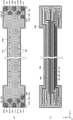
Fig. 1 is an external perspective view of a transmission line 10 according to embodiment 1.
Fig. 2 is a plan view showing an external connection portion 101 of the transmission line 10 according to embodiment 1.
Fig. 3 is an exploded plan view of the layer 1L 1 and the layer 2L 2 in the transmission line 10 according to embodiment 1.
Fig. 4 is an exploded plan view of the 3 rd layer L3 and the 4 th layer L4 in the transmission line 10 according to embodiment 1.
Fig. 5 is an exploded plan view of the 5 th layer L5 in the transmission line 10 according to embodiment 1.
Fig. 6 is a plan view schematically showing formation of a protective layer 600 in the external connection portion 101 according to embodiment 1.
Fig. 7 is a sectional view at the external connection part 101 of the transmission line 10.
Fig. 8 is an external view of the electronic device 1 in which the transmission line 10 is mounted on the circuit board 50.
Fig. 9 is a plan view showing an external connection portion 101 of the transmission line 10A according to embodiment 2.
Fig. 10 is an exploded plan view of the layer 1L 1 and the layer 2L 2 in the transmission line 10A according to embodiment 2.
Fig. 11 is an exploded plan view of the 3 rd layer L3 and the 4 th layer L4 in the transmission line 10A according to embodiment 2.
Fig. 12(a) is a plan view showing the external connection portion 101B of the transmission line 10B according to embodiment 3, fig. 12(B) is a sectional view of the 1 st electrode pad 111, and fig. 12(C) is a sectional view of the 3 rd electrode pad 131.
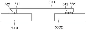
Fig. 13(a) is an external perspective view of the transmission line 10C according to embodiment 4, and fig. 13(B) is a side sectional view of the transmission line 10C connected to the circuit board 50C1 and the circuit board 50C 2.
Detailed Description
< embodiment 1 >
Fig. 1 is an external perspective view of a transmission line 10 according to embodiment 1. Fig. 2 is a plan view showing an external connection portion 101 of the transmission line 10 according to embodiment 1. Fig. 3 is an exploded plan view of the layer 1L 1 and the layer 2L 2 in the transmission line 10 according to embodiment 1. Fig. 4 is an exploded plan view of the 3 rd layer L3 and the 4 th layer L4 in the transmission line 10 according to embodiment 1. Fig. 5 is an exploded plan view of the 5 th layer L5 in the transmission line 10 according to embodiment 1. Fig. 6 is a plan view schematically showing formation of a protective layer 600 in the external connection portion 101 according to embodiment 1. Fig. 7 is a sectional view at the external connection part 101 of the transmission line 10. Fig. 8 is an external view of the electronic device 1 in which the transmission line 10 is mounted on the circuit board 50. In the drawings of the following embodiments, the dimensional relationship between the vertical and horizontal dimensions is described with appropriate emphasis, and does not necessarily coincide with the dimensional relationship between the vertical and horizontal dimensions of the actual dimensions. In order to make the drawings easy to see, some reference numerals are omitted.
The structure of the transmission line 10 will be described with reference to fig. 1. The transmission line 10 includes an external connection portion 101, a line portion 105, and an external connection portion 102. The external connection portion 101, the external connection portion 102, and the wiring portion 105 are integrally formed. External connection unit 101 is connected to one end of line unit 105, and external connection unit 102 is connected to the other end of line unit 105. The external connection portions 101 and 102 are flat plates. The line portion 105 is flat and has a shape extending in the X-axis direction (transmission line direction). In addition, the X-axis direction corresponds to the "1 st direction" and the "3 rd direction" in the present invention, and the Y-axis direction corresponds to the "2 nd direction" and the "4 th direction" in the present invention.
The ends of the external connection portions 101 and 102 in the X-axis direction on the XY plane are provided with a 1 st end E1 and a 2 nd end E2, respectively. The 1 st end E1 is an end of the transmission line 10 and is an end on the side where the external connection portions 101 and 102 are not connected to the line portion 105. The 2 nd end E2 is an end on the side where the external connection portions 101 and 102 and the line portion 105 are connected.
The 1 st region and the 2 nd region are formed on the one main surface S1 of the external connection parts 101 and 102. The 1 st region is formed on the 2 nd end E2 side of the external connection portions 101, 102. The 2 nd region is formed on the 1 st end E1 side of the external connection parts 101, 102, in other words, at the end of the transmission line 10.
A plurality of electrode pads are formed in the 1 st region and the 2 nd region, respectively. The electrode pad is used as an input-output electrode for connection with an external device. As will be described in detail later.
The transmission line 10 is made of polyimide resin or LCP, for example. Further, the transmission line 10 may be a fluororesin. More specifically, the fluororesin is Polytetrafluoroethylene (PTFE), Perfluoroalkoxyalkane (PFA), ethylene tetrafluoroethylene copolymer (ETFE), perfluoroethylene propylene copolymer (FEP). This improves chemical resistance, heat resistance, and electrical characteristics.
The detailed configuration of the transmission line 10 will be described with reference to fig. 2, 3, 4, and 5. As described above, the external connection portions 101 and 102 include the 1 st region and the 2 nd region. Although fig. 2 illustrates the external connection unit 101 as an example, the external connection unit 102 has the same configuration.
In the 1 st region of the external connection portion 101, the 1 st electrode pad 111, the 2 nd electrode pad 121, and the ground electrode 1551 are formed. In the 2 nd region, 3 rd electrode pads 131 and 132, a 4 th electrode pad 141, a ground electrode 151, and a ground electrode 1551 are formed. In addition, a ground electrode 1551 is formed at the 1 st region and the 2 nd region. The ground electrode 1551 has a shape that is connected in region 1 and region 2.
Further, ground electrode 1551 is formed over external connection unit 101, line unit 105, and external connection unit 102. Further, the ground electrode 151 and the ground electrode 1551 are connected by an electrode formed along the outer periphery.
The ground electrode 1551 may have a shape divided at a middle position of the ground electrode 1551. When the ground electrode 1551 is divided, for example, a shape connected to the inside of the transmission line 10 is preferable. In this case, since the electrode can be formed in accordance with a complicated shape and arrangement, the degree of freedom in design is improved.
(connection Structure of electrode pad)
The 1 st electrode pad 111 and the 2 nd electrode pad 121 are connected to a signal line for transmitting a high-frequency (millimeter wave) signal for 5GNR of the 1 st frequency and the 2 nd frequency according to the present invention. The 1 st signal line for transmitting a 1 st frequency high frequency signal is connected to the 1 st electrode pad 111. The 2 nd signal line 2 for transmitting a 2 nd frequency high frequency signal is connected to the 2 nd electrode pad 121. The 1 st frequency and the 2 nd frequency may be the same frequency or different frequencies.
On the other hand, the 3 rd electrode pads 131, 132, 133, 134 and the 4 th electrode pads 141, 142 are connected to a signal line for transmitting a signal for 3G, LTE of the 3 rd frequency and the 4 th frequency, a control signal line, and a power supply line according to the present invention. The 3 rd signal lines for transmitting the 3 rd frequency high frequency signal are connected to the 3 rd electrode pads 131, 132, 133, and 134. The 4 th signal line for transmitting a high frequency signal of the 4 th frequency is connected to the 4 th electrode pads 141 and 142. The 3 rd frequency and the 4 th frequency may be the same frequency or different frequencies.
In this way, the 1 st and 2 nd frequencies of the high frequency signal transmitted through the signal line connected to the 1 st and 2 nd electrode pads 111 and 121 are higher than the 3 rd and 4 th frequencies of the high frequency signal transmitted through the signal line connected to the 3 rd and 4 th electrode pads 131, 132 and 141.
The 1 st electrode pad 111, the 2 nd electrode pad 121, the 3 rd electrode pads 131, 132, and the 4 th electrode pad 141 are rectangular planar conductors, and are, for example, copper foils. The corners of these electrode pads are preferably formed in an R-chamfered shape. This can suppress coupling between the electrodes, as compared with a shape (a shape having a corner) in which no R-chamfer is formed.
(Structure of external connection part 101)
First, the structure of the external connection portion 101 will be described with reference to fig. 2, 3, 4, and 5. In the 1 st region, the 1 st electrode pad 111 and the 2 nd electrode pad 121 are disposed with a predetermined interval. More specifically, the 1 st electrode pad 111 and the 2 nd electrode pad 121 are formed along the Y-axis direction.
The outer periphery of the 1 st electrode pad 111 and the outer periphery of the 2 nd electrode pad 121 are surrounded by the ground electrode 1551 at predetermined intervals in a plan view. In particular, in the present embodiment, the 1 st electrode pad 111 and the 2 nd electrode pad 121 are surrounded by the continuous ground electrode 1551 formed on one main surface of the external connection portion 101 in a plan view.
The 1 st electrode pad 111 and the 2 nd electrode pad 121 are surrounded by the ground electrode 1551 over the entire circumference, and thus the isolation of the transmission line for transmitting the signals of the 1 st frequency and the 2 nd frequency can be sufficiently ensured. Further, since the ground electrode 1551 has a continuous shape, leakage of noise from the 1 st electrode pad 111 and the 2 nd electrode pad 121 can be suppressed. In addition, peeling of the ground electrode 1551 can be suppressed. In addition, the ground electrode 1551 has a continuous shape and is connected to the 1 st region and the 2 nd region. When the 1 st electrode pad 111 and the 2 nd electrode pad 121 are separated from each other, the interlayer connection conductor connected to the 1 st electrode pad 111 and the interlayer connection conductor connected to the 2 nd electrode pad 121 are separated from each other. This can suppress coupling between the interlayer connection conductors.
In the external connection part 101, a 3 rd electrode pad 131, a ground electrode 151, and a 3 rd electrode pad 132 are formed in this order in the Y-axis direction of the 2 nd region. The 4 th electrode pad 141 is formed to be sandwiched by the ground electrodes 1551 in the Y-axis direction of the external connection part 101.
At this time, the 3 rd electrode pads 131, 132 and the 4 th electrode pad 141 are formed at different positions in the X-axis direction. That is, the distance between the 3 rd electrode pad 131 and the 4 th electrode pad 141 becomes longer than that in the case where the 3 rd electrode pads 131, 132 and the 4 th electrode pad 141 are formed at the same position in the X-axis direction (the case where the 3 rd electrode pads 131, 132 and the 4 th electrode pad 141 are linearly arranged in the Y-axis direction). Therefore, the distance between the electrode pads can be secured, and unnecessary coupling can be suppressed.
The 3 rd electrode pad 131 is formed adjacent to the ground electrode 151 and a part of the ground electrode 1551. The 3 rd electrode pad 132 is formed adjacent to the ground electrode 151 and a part of the ground electrode 1551.
The 4 th electrode pad 141 is formed to be surrounded by the ground electrode 151 and a part of the ground electrode 1551.
Part of the outer peripheries of the 3 rd electrode pads 131 and 132 and part of the outer periphery of the 4 th electrode pad 141 are surrounded by the ground electrode 151 or the ground electrode 1551 in a plan view. In other words, the outer circumferences of the 3 rd electrode pads 131, 132 and the 4 th electrode pad 141 have portions not surrounded by the ground electrode 151 and the ground electrode 1551. Parts of the 3 rd electrode pads 131 and 132 and parts of the 4 th electrode pad 141 are surrounded by a continuous ground electrode 1551 formed on one main surface of the external connection portion 101 in a plan view.
More specifically, the ground electrode 151 or the ground electrode 1551 is not formed at least in a portion between the 3 rd electrode pad 131 and the 4 th electrode pad 141. In addition, at least a portion between the 3 rd electrode pad 132 and the 4 th electrode pad 141, the ground electrode 151 or the ground electrode 1551 is not formed.
The configurations in the 1 st region and the 2 nd region of the external connection portion 101 are compared. The leakage of the electric field of the signals of the 3 rd and 4 th frequencies is smaller than that of the signals of the 1 st and 2 nd frequencies. In this case, the signals of the 3 rd frequency and the 4 th frequency are less likely to be diffused than the signals of the 1 st frequency and the 2 nd frequency. Therefore, even if the 3 rd electrode pads 131 and 132 and the 4 th electrode pad 141 are disposed close to each other, the electrode pads are less likely to be coupled to each other than the signals of the 1 st and 2 nd frequencies.
However, in the case where the 3 rd electrode pads 131, 132 and the 4 th electrode pad 141 are close and further the ground electrode is disposed therebetween, the distance between the ground electrode and the electrode pad becomes short and the capacitive coupling becomes large. In order to suppress the increase of the capacitive coupling, the ground electrode is not disposed between the 3 rd electrode pads 131 and 132 and the 4 th electrode pad 141. That is, even if the distance between the 3 rd electrode pad 131, 132 and the 4 th electrode pad 141 in the 2 nd region is short, deterioration of the characteristics can be suppressed by not disposing the ground electrode therebetween. Further, even when the area of the 2 nd region is small, a large number of electrode pads (the 3 rd electrode pads 131, 132, and the 4 th electrode pad 141) can be arranged.
With this configuration, the area of the ground electrodes 151 and 1551 in the 2 nd region can be reduced, and the 2 nd region of the external connection unit 101 can be downsized.
Further, even if the intervals at which the 3 rd electrode pads 131, 132 and the 4 th electrode pad 141 are arranged are reduced, the deterioration of the characteristics is small. Therefore, by narrowing the distance between the 3 rd electrode pad 131 and the 4 th electrode pad 141, a large number of the 3 rd electrode pads 131 and 132 and the 4 th electrode pad 141 can be arranged in the 2 nd region.
(construction of external connection part 102)
Next, the structure of the external connection portion 102 will be described with reference to fig. 3 and 4. The 1 st electrode pad 112 and the 2 nd electrode pad 122 are disposed with a predetermined interval in the 1 st region. More specifically, the 1 st electrode pad 112 and the 2 nd electrode pad 122 are formed along the Y-axis direction.
The outer periphery of the 1 st electrode pad 112 and the outer periphery of the 2 nd electrode pad 122 are surrounded by the ground electrode 1551 at a given interval in a plan view.
Since the 1 st electrode pad 112 and the 2 nd electrode pad 122 are surrounded by the ground electrode 1551 over the entire circumference, the isolation of the transmission line for transmitting the 1 st frequency signal and the 2 nd frequency signal can be sufficiently ensured.
In the Y-axis direction of the 2 nd region in the external connection portion 102, a 3 rd electrode pad 133, a ground electrode 152, and a 3 rd electrode pad 134 are formed in this order. In the Y-axis direction of the external connection portion 101, the 4 th electrode pad 142 is formed to be sandwiched by the ground electrodes 1551.
At this time, the 3 rd electrode pads 133 and 134 and the 4 th electrode pad 142 are formed at different positions in the X-axis direction. That is, the distance between the 3 rd electrode pads 133 and 134 and the 4 th electrode pad 142 is longer than that in the case where the 3 rd electrode pads 133 and 134 and the 4 th electrode pad 142 are formed at the same position in the X-axis direction (the case where the 3 rd electrode pads 133 and 134 and the 4 th electrode pad 142 are linearly arranged in the Y-axis direction). Therefore, the distance between the electrode pads can be secured, and unnecessary coupling can be suppressed.
The 3 rd electrode pad 133 is formed adjacent to the ground electrode 152 and a part of the ground electrode 1551. The 3 rd electrode pad 134 is formed adjacent to the ground electrode 152 and a part of the ground electrode 1551.
The 4 th electrode pad 142 is formed to be surrounded by the ground electrode 152 and a part of the ground electrode 1551.
Part of the outer peripheries of the 3 rd electrode pads 133 and 134 and part of the outer periphery of the 4 th electrode pad 142 are surrounded by the ground electrode 152 or the ground electrode 1551 in a plan view. In other words, the outer peripheries of the 3 rd electrode pads 133, 134 and the 4 th electrode pad 142 have portions not surrounded by the ground electrode 152 and the ground electrode 1551, respectively.
More specifically, the ground electrode 152 or the ground electrode 1551 is not formed at least in a portion between the 3 rd electrode pad 133 and the 4 th electrode pad 142 and at least in a portion between the 3 rd electrode pad 134 and the 4 th electrode pad 142.
The configurations in the 1 st region and the 2 nd region of the external connection portion 102 are compared. As described above, the leakage of the electric field of the signals of the 3 rd and 4 th frequencies is smaller than the signals of the 1 st and 2 nd frequencies. In this case, the signals of the 3 rd frequency and the 4 th frequency are less likely to be diffused than the signals of the 1 st frequency and the 2 nd frequency. Therefore, even if the 3 rd electrode pads 133 and 134 and the 4 th electrode pad 142 are disposed close to each other, the electrode pads are less likely to be coupled to each other than the signals of the 1 st and 2 nd frequencies.
However, in the case where the 3 rd electrode pads 133, 134 and the 4 th electrode pad 142 are close and further the ground electrode is disposed therebetween, the distance between the ground electrode and the electrode pad becomes short and the capacitive coupling becomes large. In order to suppress the increase of the capacitive coupling, the ground electrode is not disposed between the 3 rd electrode pads 133 and 134 and the 4 th electrode pad 142. That is, even if the distance between the 3 rd electrode pads 133, 134 and the 4 th electrode pad 142 in the 2 nd region is short, deterioration of the characteristics can be suppressed by not disposing the ground electrode therebetween. Further, even when the area of the 2 nd region is small, a large number of electrode pads (the 3 rd electrode pads 133 and 134 and the 4 th electrode pad 142) can be arranged.
With this configuration, the area of the ground electrodes 152 and 1551 in the 2 nd region can be reduced. Therefore, the size of the 2 nd region of the external connection portion 102 can be reduced.
Further, even if the intervals between the 3 rd electrode pads 133, 134 and the 4 th electrode pad 142 are reduced, the deterioration of the characteristics is small. Therefore, by narrowing the distance between the 3 rd electrode pad 132 and the 4 th electrode pad 142, the 3 rd electrode pads 133 and 134 and the 4 th electrode pad 142 can be arranged in the 2 nd region in a large number.
(Structure of transmission line 10)
A more specific structure of the transmission line 10 will be explained. As shown in fig. 3, 4, and 5, the transmission line 10 is formed by stacking a 1 st layer L1, a 2 nd layer L2, a 3 rd layer L3, a 4 th layer L4, and a 5 th layer L5.
As described above, the 1 st electrode pads 111, 112, the 2 nd electrode pads 121, 122, the 3 rd electrode pads 131, 132, 133, 134, the 4 th electrode pads 141, 142, and the ground electrodes 151, 152, 1551 are formed on the 1 st layer L1.
In the 2 nd layer L2, connection pads 301, 303, 304, 305, 307, 308, a ground electrode 1552, a signal line 210, and a signal line 220 are formed. The interlayer connection conductors 1312, 1322, 1332, 1342, 1412, 1422 and the plurality of interlayer connection conductors 702 are formed in the 2 nd layer L2. The interlayer connection conductors 1312, 1322, 1332, 1342, 1412, 1422 and 702 are formed by filling through holes with a conductive paste and curing the same, for example.
The signal line 210 and the signal line 220 are strip-shaped (linear) conductors having substantially the same shape, and are arranged substantially in parallel. In addition, the signal line 210 corresponds to the "1 st signal line" of the present invention, and the signal line 220 corresponds to the "2 nd signal line" of the present invention.
In the 3 rd layer L3, connection pads 311, 313, 314, 315, 317, 318 and a ground electrode 1553 are formed. In addition, interlayer connection conductors 1313, 1323, 1333, 1343, 1413, 1423, 1513, 1523 and a plurality of interlayer connection conductors 703 are formed in the 3 rd layer L3. The interlayer connection conductors 1313, 1323, 1333, 1343, 1413, 1423, 1513, 1523 and the interlayer connection conductor 703 are formed by filling a through hole with a conductive paste and curing, for example.
The 4 th layer L4 includes a signal line 410, a signal line 420, a signal line 430, and a ground electrode 1554. In addition, a plurality of interlayer connection conductors 704 are formed in the 4 th layer L4, and the interlayer connection conductors 704 are formed by filling a through hole with a conductive paste and curing the conductive paste, for example. The signal line 410 and the signal line 430 are strip-shaped (linear) conductors having substantially the same shape. The signal lines 410, 420, and 430 are arranged substantially in parallel.
In addition, any of the signal lines 410, 420, and 430 corresponds to the "3 rd signal line" or the "4 th signal line" of the present invention.
The 5 th layer L5 is provided with a ground electrode 1555.
In fig. 3, 4, and 5, the interlayer connection conductors 701, 702, 703, and 704 for grounding in the external connection portions 101 and 102 are omitted for easy illustration.
(connection structure of 1 st electrode pads 111, 112 and Signal line 210)
The interlayer connection conductor 1111 is connected to the 1 st electrode pad 111. The interlayer connection conductor 1121 is connected to the 1 st electrode pad 112.
One end of the signal line 210 is connected to the 1 st electrode pad 111 via the interlayer connection conductor 1111. The other end of the signal line 210 is connected to the 1 st electrode pad 112 via the interlayer connection conductor 1121. Thereby, the signal line 210 connects the 1 st electrode pad 111 and the 1 st electrode pad 112 at both ends of the transmission line 10.
(connection structure of No. 2 electrode pads 121, 122 and Signal line 220)
The interlayer connection conductor 1211 is connected to the 2 nd electrode pad 121. The 2 nd electrode pad 122 is connected to an interlayer connection conductor 1221.
One end of the signal line 220 is connected to the 2 nd electrode pad 121 via an interlayer connection conductor 1211. The other end of the signal line 220 is connected to the 2 nd electrode pad 122 via an interlayer connection conductor 1221. Thereby, the signal line 220 connects the 2 nd electrode pad 121 and the 2 nd electrode pad 122 at both ends of the transmission line 10.
(connection structure of 3 rd electrode pads 131, 133 and Signal line 410)
The 3 rd electrode pad 131 is connected to the connection pad 301 via an interlayer connection conductor 1311. The connection pad 301 is connected to the connection pad 311 via an interlayer connection conductor 1312. The connection pad 311 is connected to one end of the signal line 410 via an interlayer connection conductor 1313.
The 3 rd electrode pad 133 is connected to the connection pad 305 via an interlayer connection conductor 1331. The connection pad 305 is connected to the connection pad 315 via an interlayer connection conductor 1332. The connection pad 315 is connected to the other end of the signal line 410 via an interlayer connection conductor 1333.
Thereby, the signal line 410 connects the 3 rd electrode pad 131 and the 3 rd electrode pad 133 at both ends of the transmission line 10.
(connection structure of No. 3 electrode pads 132, 134 and Signal line 430)
The 3 rd electrode pad 132 is connected to the connection pad 303 via the interlayer connection conductor 1321. The connection pads 303 are connected to the connection pads 313 via interlayer connection conductors 1322. The connection pad 313 is connected to one end of the signal line 430 via the interlayer connection conductor 1323.
The 3 rd electrode pad 134 is connected to the connection pad 307 via an interlayer connection conductor 1341. The connection pad 307 is connected to the connection pad 317 via an interlayer connection conductor 1342. The connection pad 317 is connected to the other end of the signal line 430 via an interlayer connection conductor 1343.
Thereby, the signal line 430 connects the 3 rd electrode pad 132 and the 3 rd electrode pad 134 at both ends of the transmission line 10.
(connection structure of 4 th electrode pads 141, 142 and signal line 420)
The 4 th electrode pad 141 is connected to the connection pad 304 via the interlayer connection conductor 1411. The connection pad 304 is connected to the connection pad 314 via an interlayer connection conductor 1412. The connection pad 314 is connected to one end of the signal line 420 via an interlayer connection conductor 1413.
The 4 th electrode pad 142 is connected to the connection pad 308 via the interlayer connection conductor 1421. The connection pad 308 is connected to the connection pad 318 via the interlayer connection conductor 1422. The connection pad 318 is connected to the other end of the signal line 420 via the interlayer connection conductor 1423.
Thereby, the signal line 420 connects the 4 th electrode pad 141 and the 4 th electrode pad 142 at both ends of the transmission line 10.
In the above configuration, the 3 rd electrode pads 131, 132, 133, and 134 are formed on the 1 st end E1 side (end side of the transmission line 10) of the 4 th electrode pads 141 and 142.
In this case, when the frequency of the high frequency signal transmitted through the signal line 410 or 430 is different from the frequency of the high frequency signal transmitted through the signal line 420, it is preferable that the frequency of the transmission line connected to the 3 rd electrode pad 131, 132, 133, or 134 is lower than the frequency of the transmission line connected to the 4 th electrode pad 141 or 142. More specifically, the frequency of the signal lines 410, 430 is preferably lower than the frequency of the signal line 420.
With such a configuration, transmission loss in the signal lines 420 can be suppressed, and unnecessary coupling between the signal lines and between the ground electrodes can be suppressed.
(connection structure of ground electrode 151)
In the 1 st layer L1, an interlayer connection conductor 1511 is connected to the ground electrode 151. In the 2 nd layer L2, an interlayer connection conductor 1512 is connected to the ground electrode 1552. In the 3 rd layer L3, an interlayer connection conductor 1513 is connected to the ground electrode 1553.
The ground electrode 151 is connected to a ground electrode 1552 via an interlayer connection conductor 1511. The ground electrode 1552 is connected to a ground electrode 1553 via an interlayer connection conductor 1512. The ground electrode 1553 is connected to a ground electrode 1554 via an interlayer connection conductor 1513.
(connection structure of ground electrode 152)
In the 1 st layer L1, an interlayer connection conductor 1521 is connected to the ground electrode 152. In the 2 nd layer L2, an interlayer connection conductor 1522 is connected to the ground electrode 1552. In the 3 rd layer L3, an interlayer connection conductor 1523 is connected to the ground electrode 1553.
The ground electrode 152 is connected to a ground electrode 1552 via an interlayer connection conductor 1521. The ground electrode 1552 is connected to a ground electrode 1553 via an interlayer connection conductor 1522. The ground electrode 1552 is connected to a ground electrode 1554 via an interlayer connection conductor 1523.
(connection structure of other interlayer connection conductor for grounding)
The interlayer connection conductor 701 formed in the ground electrode 1551 of the 1 st layer L1 is connected to the ground electrode 1552 of the 2 nd layer L2. The interlayer connection conductor 702 formed on the ground electrode 1552 of the 2 nd layer L2 is connected to the ground electrode 1553 of the 3 rd layer L3. The interlayer connection conductor 703 formed in the ground electrode 1553 of the 3 rd layer L3 is connected to the ground electrode 1554 of the 4 th layer L4. The interlayer connection conductor 704 formed on the ground electrode 1554 of the 4 th layer L4 is connected to the ground electrode 1555 of the 5 th layer L5.
By forming the interlayer connection conductors 701, 702, 703, and 704 in this manner, it is possible to suppress noise from being radiated to the outside from the signal lines 210, 220, 410, 420, and 430 of the transmission line 10.
(exposed area of electrode pad)
The structure in which the protective layer 600 is formed on the transmission line 10 will be described with reference to the external connection portion 101 shown in fig. 6. In fig. 6, the openings 601, 602, 603, 604, 605, 606 are shown by solid lines. The protective layer 600 has openings 601, 602, 603, 604, 605, 606 in the external connection portion 101. The opening 601 is formed to overlap the 1 st electrode pad 111 in a plan view. The opening 602 is formed to overlap with the 2 nd electrode pad 121 in a plan view. The opening 603 is formed to overlap with the 3 rd electrode pad 131 in a plan view. The opening 604 is formed to overlap with the 3 rd electrode pad 132 in a plan view. The opening 605 is formed to overlap the ground electrodes 151 and 1551 in a plan view. The opening 606 is formed to overlap with the 4 th electrode pad 141 in a plan view.
The opening 601 has substantially the same shape as the 1 st electrode pad 111. The opening 602 has substantially the same shape as the 2 nd electrode pad 121. The opening 603 is smaller in shape than the 3 rd electrode pad 131. The opening 604 is smaller in shape than the 3 rd electrode pad 132. Opening 603 is the same shape as openings 604, 605, 606. The opening 606 is smaller in shape than the 4 th electrode pad 141.
By providing such a protective layer 600, short-circuiting between electrode pads when the transmission line 10 is mounted on a circuit board with solder or the like can be suppressed. Further, by configuring the opening formed in the protective layer 600 as described above, the bonding area of the 1 st electrode pad 111 and the 2 nd electrode pad 121 can be increased when the transmission line 10 is mounted. On the other hand, in the 3 rd electrode pads 131, 132, the 4 th electrode pad 141, and the ground electrodes 151, 1551, even if the 3 rd electrode pads 131, 132, and the 4 th electrode pad 141 are short in distance, the above-described short circuit between the electrode pads when the transmission line 10 is mounted can be suppressed by the openings 602, 603, 604, 605, and the isolation can be ensured.
Fig. 7 is a sectional view taken along line X1-X1 in fig. 6. In fig. 6, the X1-X1 line passes through the 3 rd electrode pad 131, the 1 st electrode pad 111, and the signal line 210 in the 1 st layer L1 and the 2 nd layer L2, and passes through the 3 rd electrode pad 131, the 1 st electrode pad 111, and the signal line 410 in the 1 st layer L1, the 2 nd layer L2, the 3 rd layer L3, and the 4 th layer L4.
As shown in fig. 7, the signal line 210 is disposed on the side of the first main surface S1 with respect to the signal line 410, and is connected to the electrode pad on the first main surface S1 using interlayer connection conductors extending in the thickness direction.
That is, the length from the signal line 210 transmitting the signals of the 1 st and 2 nd frequencies to the 1 st electrode pad 111 (hereinafter, the 1 st transmission line length) is shorter than the length from the signal line 410 transmitting the signals of the 3 rd and 4 th frequencies to the 3 rd electrode pad 131 (hereinafter, the 2 nd transmission line length). More specifically, the 1 st transmission line length is shorter than the 2 nd transmission line length by an amount corresponding to the lengths of the interlayer connection conductors 1312 and 1313.
The interlayer connection conductor has a small line width, uses a material having high conductor resistance for connection, and is easily affected from the outside because it is difficult to shield the periphery of the transmission line. However, with this configuration, the line length of the transmission line for the high-frequency signals of the 1 st and 2 nd frequencies having a high frequency can be made shorter than the line length of the transmission line for the high-frequency signals of the 3 rd and 4 th frequencies, and the above-described adverse effect can be suppressed, and in particular, the transmission loss (insertion loss) of the transmission line for the high-frequency signals of the 1 st and 2 nd frequencies that are susceptible to the adverse effect can be reduced. Further, since the 1 st transmission line length is shorter than the 2 nd transmission line length, the loss due to the impedance mismatch can be reduced.
Fig. 8 is a perspective view of the transmission line 10 mounted on the circuit board 50. The electronic device 1 includes the transmission line 10, the surface-mounted components 81 and 82, and the circuit board 50.
The transmission line 10 is directly mounted on the circuit board 50 using a conductive bonding material such as solder. More specifically, the 1 st electrode pads 111, 112, the 2 nd electrode pads 121, 122, the 3 rd electrode pads 131, 132, 133, 134, and the 4 th electrode pads 141, 142 are mounted on the circuit substrate 50 via solder or the like.
By using this structure, the transmission line 10 can be downsized, and can be disposed in a small space while avoiding surface-mounted components. Further, even in the case where the number of signal lines (the number of electrode pads) is increased and the distance between the electrode pads is shortened, the electronic device 1 using the transmission line in which unnecessary coupling is suppressed without increasing the size of the external connection portions 101, 102 can be realized.
< embodiment 2 >
The transmission line according to embodiment 2 will be described with reference to fig. 2. Fig. 9 is a plan view showing an external connection portion 101 of the transmission line 10A according to embodiment 2. Fig. 10 is an exploded plan view of the layer 1L 1 and the layer 2L 2 in the transmission line 10A according to embodiment 2. Fig. 11 is an exploded plan view of the 3 rd layer L3 and the 4 th layer L4 in the transmission line 10A according to embodiment 2. In fig. 11, the interlayer connection conductor 704 in the 5 th layer L5 and the 4 th layer L4 are not shown for the sake of easy illustration.
The transmission line 10A in the present embodiment is different from the transmission line 10 according to embodiment 1 in that: the external connection portion 101 includes the 3 rd electrode pads 135 and 136, the external connection portion 102 includes 137 and 138, the external connection portion 101 includes the 4 th electrode pad 145, the external connection portion 102 includes the 4 th electrode pad 146, the ground electrodes 153, 154, 156 and 157, the signal lines 440, 450 and 460 are provided, and a plurality of connection pads and interlayer connection conductors are provided at different points according to the difference, the positional relationship between the 1 st electrode pad 111 and the 2 nd electrode pad 121 in the external connection portion 101, the positional relationship between the 1 st electrode pad 112 and the 2 nd electrode pad 122 in the external connection portion 102, and the boundary line between the 1 st region and the 2 nd region is not parallel to the Y-axis direction. The other configuration of the transmission line 10A is the same as that of the transmission line 10 according to embodiment 1, and the description of the same parts is omitted.
In the 1 st region of the external connection portion 101, the 1 st electrode pad 111, the 2 nd electrode pad 121, and the ground electrode 1551 are formed. In the 2 nd region, 3 rd electrode pads 131, 132, 135, 136, 4 th electrode pads 141, 145, ground electrodes 151, 153, 154, and ground electrode 1551 are formed. The ground electrodes 151, 153, 154 and the ground electrode 1551 are connected by electrodes formed along the outer circumference.
In the 1 st region of the external connection portion 102, the 1 st electrode pad 112, the 2 nd electrode pad 122, and the ground electrode 1551 are formed. In the 2 nd region, 3 rd electrode pads 133, 134, 137, and 138, 4 th electrode pads 142 and 146, ground electrodes 152, 156, and 157, and a ground electrode 1551 are formed. The ground electrodes 152, 156, 157 and the ground electrode 1551 are connected by electrodes formed along the outer circumference.
(structure of the 1 st region)
First, the structure of the external connection portion 101 will be described. The 1 st electrode pad 111 and the 2 nd electrode pad 121 are disposed with a predetermined interval in the 1 st region. The outer periphery of the 1 st electrode pad 111 and the outer periphery of the 2 nd electrode pad 121 are surrounded by the ground electrode 1551 at predetermined intervals in a plan view.
The 1 st electrode pad 111 and the 2 nd electrode pad 121 are formed at different positions in an X-axis direction (1 st direction) and a Y-axis direction (2 nd direction).
The 1 st electrode pad 111 and the 2 nd electrode pad 121 are surrounded by the ground electrode 1551 over the entire circumference, and thus the isolation of the transmission line for transmitting the signals of the 1 st frequency and the 2 nd frequency can be sufficiently ensured.
Next, the structure of the external connection portion 102 will be described. The 1 st electrode pad 112 and the 2 nd electrode pad 122 are disposed with a predetermined interval in the 1 st region. The outer periphery of the 1 st electrode pad 112 and the outer periphery of the 2 nd electrode pad 122 are surrounded by the ground electrode 1551 at a given interval in a plan view.
The 1 st electrode pad 112 and the 2 nd electrode pad 122 are formed at different positions in the X-axis direction (1 st direction) and the Y-axis direction (2 nd direction).
The 1 st electrode pad 112 and the 2 nd electrode pad 122 are surrounded by the ground electrode 1551 over the entire circumference, and the isolation of the transmission line for transmitting the signals of the 1 st frequency and the 2 nd frequency can be sufficiently ensured.
The 1 st electrode pad 111 and the 2 nd electrode pad 121, and the 1 st electrode pad 112 and the 2 nd electrode pad 122 are formed at different positions in the X-axis direction and the Y-axis direction, whereby the distance between the 1 st electrode pad 111 and the 2 nd electrode pad 121, and the distance between the 1 st electrode pad 112 and the 2 nd electrode pad 122 become longer than those in the case where they are formed at the same position in the X-axis direction. Therefore, the distance between the electrode pads can be secured, and unnecessary coupling can be suppressed.
(Structure of 2 nd region)
In the 2 nd region of the external connection part 101, the 3 rd electrode pads 131, 132, 135, 136 and the 4 th electrode pads 141, 145 are arranged with a given interval.
In the 2 nd region of the external connection portion 102, the 3 rd electrode pads 133, 134, 137, 138 and the 4 th electrode pads 142, 146 are arranged with a given interval therebetween.
First, the structure of the external connection portion 101 will be described. In the Y-axis direction of the external connection portion 101, a 3 rd electrode pad 132, a ground electrode 151, a 3 rd electrode pad 131, a ground electrode 153, and a 3 rd electrode pad 135 are formed in this order.
Similarly, in the Y-axis direction of the external connection portion 101, the ground electrode 154, the 4 th electrode pad 141, a part of the ground electrode 1551, the 4 th electrode pad 145, and a part of the ground electrode 1551 are formed in this order. Further, the 3 rd electrode pad 136 is formed on the 2 nd end E2 side of the ground electrode 154.
That is, the 3 rd electrode pad 131 is formed adjacent to the ground electrode 151, the ground electrode 153, and a part of the ground electrode 1551. The 3 rd electrode pad 132 is formed adjacent to the ground electrodes 151 and 154. The 3 rd electrode pad 135 is formed adjacent to the ground electrode 153 and a part of the ground electrode 1551.
The 4 th electrode pad 141 is formed to be surrounded by the ground electrode 151, the ground electrode 154, and a part of the ground electrode 1551. The 4 th electrode pad 145 is formed to be surrounded by the ground electrodes 153 and 1551. The 3 rd electrode pad 136 is formed to be surrounded by the ground electrode 154 and a portion of the ground electrode 1551.
At this time, the 3 rd electrode pads 131, 132, 135 and the 4 th electrode pads 141, 145 are formed at different positions in the X-axis direction (1 st direction) and the Y-axis direction (2 nd direction). In addition, the 4 th electrode pads 141, 145 and the 3 rd electrode pad 136 are formed at different positions in the X-axis direction (1 st direction) and the Y-axis direction (2 nd direction).
Thus, the distance between the 3 rd electrode pads 131, 132, 135 and the 4 th electrode pads 141, 145 and the distance between the 4 th electrode pads 141, 145 and the 3 rd electrode pad 136 can be sufficiently secured.
Next, the structure of the external connection portion 102 will be described. In the Y-axis direction of the external connection portion 102, a 3 rd electrode pad 134, a ground electrode 152, a 3 rd electrode pad 133, a ground electrode 156, and a 3 rd electrode pad 137 are formed in this order.
Similarly, the ground electrode 157, the 4 th electrode pad 142, a part of the ground electrode 1551, the 4 th electrode pad 146, and a part of the ground electrode 1551 are formed in this order in the Y-axis direction of the external connection portion 102. Further, the 3 rd electrode pad 138 is formed on the 2 nd end E2 side of the ground electrode 157.
That is, the 3 rd electrode pad 134 is formed adjacent to the ground electrodes 152 and 157. The 3 rd electrode pad 133 is formed adjacent to the ground electrode 152, a part of the ground electrode 1551, and the ground electrode 156. The 3 rd electrode pad 137 is formed adjacent to the ground electrode 156, a part of the ground electrode 1551.
The 4 th electrode pad 142 is formed to be surrounded by the ground electrode 152, a part of the ground electrode 1551, and the ground electrode 157. The 4 th electrode pad 146 is formed to be surrounded by a ground electrode 156, a part of the ground electrode 1551.
The 3 rd electrode pad 138 is formed to be surrounded by a portion of the ground electrode 1551 and the ground electrode 157.
At this time, the 3 rd electrode pads 133, 134, 137 and the 4 th electrode pads 142, 146 are formed at different positions in the X-axis direction (1 st direction) and the Y-axis direction (2 nd direction). In addition, the 4 th electrode pads 142 and 146 and the 3 rd electrode pad 138 are formed at different positions in the X-axis direction (1 st direction) and the Y-axis direction (2 nd direction).
Thus, the distance between the 3 rd electrode pads 133, 134, 137 and the 4 th electrode pads 142, 146 and the distance between the 4 th electrode pads 142, 146 and the 3 rd electrode pad 138 can be sufficiently secured.
According to the above-described structure, the outer circumferences of the 3 rd electrode pads 131, 132, 133, 134, 135, 136, 137, 138 have portions not surrounded by the ground electrodes 151, 152, 153, 154, 156, 157, 1551, respectively. Similarly, the 4 th electrode pads 141, 142, 145, and 146 have portions not surrounded by the ground electrodes 151, 152, 153, 154, 156, 157, and 1551 on the outer peripheries thereof, respectively.
The configurations in region 1 and region 2 are compared. The leakage of the electric field of the signals of the 3 rd and 4 th frequencies is smaller than that of the signals of the 1 st and 2 nd frequencies. In this case, the signals of the 3 rd frequency and the 4 th frequency are less likely to be diffused than the signals of the 1 st frequency and the 2 nd frequency. Therefore, even if the 3 rd electrode pads 131, 132, 133, 134, 135, 136, 137, 138 and the 4 th electrode pads 141, 142, 145, 146 are disposed close to each other, the coupling between the electrode pads is less likely to occur compared to the signals of the 1 st frequency and the 2 nd frequency.
However, in the case where the 3 rd electrode pads 131, 132, 133, 134, 135, 136, 137, 138 and the 4 th electrode pads 141, 142, 145, 146 are close and further the ground electrode is disposed therebetween, the distance between the ground electrode and the electrode pads becomes short and the capacitive coupling becomes large. In order to suppress the increase of the capacitive coupling, the ground electrode is not provided in part. That is, even if the distance between the 3 rd electrode pad 131, 132, 133, 134, 135, 136, 137, 138 and the 4 th electrode pad 141, 142, 145, 146 in the 2 nd region is short, it is possible to suppress deterioration of characteristics by not disposing the ground electrode therebetween. Further, even when the area of the 2 nd region is small, a large number of electrode pads (the 3 rd electrode pads 131, 132, 133, 134, 135, 136, 137, 138, and the 4 th electrode pads 141, 142, 145, 146) can be arranged.
By providing this structure, the area of the ground electrodes 151, 152, 153, 154, 156, 157, 1551 in the 2 nd region can be reduced. Therefore, the size of the 2 nd region can be reduced.
Further, even if the intervals at which the 3 rd electrode pads 131, 132, 133, 134, 135, 136, 137, 138 and the 4 th electrode pads 141, 142, 145, 146 are arranged are reduced, the deterioration of the characteristics is small. Therefore, by narrowing the distance between the 3 rd electrode pads 131 and 132 and the 4 th electrode pads 141, 142, 145, and 146, a large number of the 3 rd electrode pads 131 and 132 and the 4 th electrode pads 141, 142, 145, and 146 can be arranged in the 2 nd region.
(positional relationship of electrode pad)
The positional relationship of the electrode pads formed in the 1 st region and the 2 nd region will be described more specifically with reference to fig. 9. The 1 st electrode pad 111, the 2 nd electrode pad 121, the 3 rd electrode pad 135, and the 4 th electrode pad 145 will be described as an example. As shown in fig. 9, the boundary between the 1 st region and the 2 nd region is not parallel to the Y-axis direction. Even with this configuration, the size of the 2 nd region can be reduced.
An angle formed by a straight line connecting the 1 st electrode pad 111 and the 2 nd electrode pad 121 and a straight line parallel to the Y-axis direction is represented by θ 1, and an angle formed by a straight line connecting the 3 rd electrode pad 135 and the 4 th electrode pad 145 and a straight line parallel to the Y-axis direction is represented by θ 2.
In this case, the 1 st electrode pad 111, the 2 nd electrode pad 121, the 3 rd electrode pad 135, and the 4 th electrode pad 145 are preferably arranged such that the angle θ 1 and the angle θ 2 are substantially the same. Thus, the distances between the 1 st electrode pad 111, the 2 nd electrode pad 121, the 3 rd electrode pad 135, and the 4 th electrode pad 145 can be sufficiently secured, and the coupling of the transmission line of the high-frequency signals of the 1 st frequency and the 2 nd frequency and the transmission line of the high-frequency signals of the 3 rd frequency and the 4 th frequency can be suppressed.
(Structure of Transmission line 10A)
Next, the structure of the transmission line 10A will be described. As shown in fig. 10 and 11, the transmission line 10A is formed by stacking a 1 st layer L1, a 2 nd layer L2, a 3 rd layer L3, a 4 th layer L4, and a 5 th layer L5 (not shown).
The external connection portion 102 of the 1 st layer L1 has interlayer connection conductors 1121, 1221, 1331, 1341, 1371, 1381, 1421, 1461, 1521, 1561, and 1571 formed therein. The interlayer connection conductors 1121, 1221, 1331, 1341, 1371, 1381, 1421, 1461, 1521, 1561, and 1571 are formed by filling through holes with a conductive paste and curing the paste, for example.
The layer 4L 4 includes a signal line 410, a signal line 420, a signal line 430, a signal line 440, a signal line 450, and a signal line 460. The signal lines 410, 420, 430, 440, 450, and 460 are disposed at substantially parallel positions.
(connection Structure of No. 1 electrode pad and Signal line 210, No. 2 electrode pad and Signal line 220)
As shown in the above-described embodiment, the signal line 210 is connected to the 1 st electrode pad 111 and the 1 st electrode pad 112. The signal line 220 is connected to the 2 nd electrode pad 121 and the 2 nd electrode pad 122.
Further, the signal line 410 connects the 3 rd electrode pad 131 and the 3 rd electrode pad 133. The signal line 420 connects the 4 th electrode pad 141 and the 4 th electrode pad 142. The signal line 430 connects the 3 rd electrode pad 132 and the 3 rd electrode pad 134.
(connection structure of 3 rd electrode pads 135, 137 and signal line 440)
The 3 rd electrode pad 135 is connected to the connection pad 350 via the interlayer connection conductor 1351. The connection pad 350 is connected to the connection pad 360 via the interlayer connection conductor 1352. The connection pad 360 is connected to one end of the signal line 440 via the interlayer connection conductor 1353.
The 3 rd electrode pad 137 is connected to the connection pad 355 via an interlayer connection conductor 1371. The connection pad 355 is connected to the connection pad 365 via an interlayer connection conductor 1372. The connection pad 365 is connected to the other end of the signal line 440 via an interlayer connection conductor 1373.
Thereby, the signal line 440 connects the 3 rd electrode pad 135 and the 3 rd electrode pad 137 at both ends of the transmission line 10A.
(connection structure of 3 rd electrode pads 136, 138 and Signal line 460)
The 3 rd electrode pad 136 is connected to the connection pad 354 via an interlayer connection conductor 1361. The connection pad 354 is connected to the connection pad 364 via an interlayer connection conductor 1362. The connection pad 364 is connected to one end of the signal line 460 via an interlayer connection conductor 1363.
The 3 rd electrode pad 138 is connected to the connection pad 359 via an interlayer connection conductor 1381. The connection pad 359 is connected to the connection pad 369 via an interlayer connection conductor 1382. The connection pad 369 is connected to the other end of the signal line 460 via an interlayer connection conductor 1383.
Thereby, the signal line 460 connects the 3 rd electrode pad 136 and the 3 rd electrode pad 138 at both ends of the transmission line 10A.
(connection structure of 4 th electrode pads 145 and 146 and signal line 450)
The 4 th electrode pad 145 is connected to the connection pad 352 via an interlayer connection conductor 1451. The connection pad 352 is connected to the connection pad 362 via the interlayer connection conductor 1452. The connection pad 362 is connected to one end of the signal line 450 via an interlayer connection conductor 1453.
The 4 th electrode pad 146 is connected to the connection pad 357 through an interlayer connection conductor 1461. The connection pad 357 is connected to the connection pad 367 via the interlayer connection conductor 1462. The connection pad 367 is connected to the other end of the signal line 450 via the interlayer connection conductor 1463.
Thereby, the signal line 450 connects the 4 th electrode pad 145 and the 4 th electrode pad 146 at both ends of the transmission line 10A.
(connection structure of ground electrode)
As in the above-described embodiment, the ground electrode 151 is connected to the ground electrode 1552 via the interlayer connection conductor 1511. The ground electrode 1552 is connected to a ground electrode 1553 via an interlayer connection conductor 1512. The ground electrode 1553 is connected to a ground electrode 1554 via an interlayer connection conductor 1513.
The ground electrode 152 is connected to a ground electrode 1552 via an interlayer connection conductor 1521. The ground electrode 1552 is connected to a ground electrode 1553 via an interlayer connection conductor 1522. The ground electrode 1553 is connected to a ground electrode 1554 via an interlayer connection conductor 1523.
(connection structure of ground electrode 153)
In the 1 st layer L1, an interlayer connection conductor 1531 is connected to the ground electrode 153. In the 2 nd layer L2, an interlayer connection conductor 1532 is connected to the ground electrode 1552. In the 3 rd layer L3, an interlayer connection conductor 1533 is connected to the ground electrode 1553.
The ground electrode 153 is connected to a ground electrode 1552 via an interlayer connection conductor 1531. The ground electrode 1552 is connected to a ground electrode 1553 via an interlayer connection conductor 1532. The ground electrode 1553 is connected to a ground electrode 1554 via an interlayer connection conductor 1533.
(connection structure of ground electrode 154)
In the 1 st layer L1, an interlayer connection conductor 1541 is connected to the ground electrode 154. In the 2 nd layer L2, an interlayer connection conductor 1542 is connected to the ground electrode 1552. In the 3 rd layer L3, an interlayer connection conductor 1543 is connected to the ground electrode 1553.
The ground electrode 154 is connected to a ground electrode 1552 via an interlayer connection conductor 1541. The ground electrode 1552 is connected to a ground electrode 1553 via an interlayer connection conductor 1542. The ground electrode 1553 is connected to a ground electrode 1554 via an interlayer connection conductor 1543.
(connection structure of ground electrode 156)
In the 1 st layer L1, an interlayer connection conductor 1561 is connected to the ground electrode 156. In the 2 nd layer L2, an interlayer connection conductor 1562 is connected to the ground electrode 1552. In the 3 rd layer L3, an interlayer connection conductor 1563 is connected to the ground electrode 1553.
The ground electrode 156 is connected to a ground electrode 1552 via an interlayer connection conductor 1561. The ground electrode 1552 is connected to a ground electrode 1553 via an interlayer connection conductor 1562. The ground electrode 1553 is connected to a ground electrode 1554 via an interlayer connection conductor 1563.
(connection structure of ground electrode 157)
In the 1 st layer L1, an interlayer connection conductor 1571 is connected to the ground electrode 157. In the layer 2L 2, an interlayer connection conductor 1572 is connected to the ground electrode 1552. In the 3 rd layer L3, an interlayer connection conductor 1573 is connected to the ground electrode 1553.
The ground electrode 157 is connected to a ground electrode 1552 via an interlayer connection conductor 1571. The ground electrode 1552 is connected to a ground electrode 1553 via an interlayer connection conductor 1572. The ground electrode 1553 is connected to a ground electrode 1554 via an interlayer connection conductor 1573.
Even with this configuration, it is possible to provide a transmission line in which unnecessary coupling is suppressed without increasing the size of the external connection portions 101 and 102. Further, by forming the 1 st electrode pad 111 and the 2 nd electrode pad 121 at different positions in the X-axis direction, the distance between the electrode pads can be secured, and unnecessary coupling can be suppressed.
In the above configuration, the number of the 1 st electrode pad, the 2 nd electrode pad, the 3 rd electrode pad, and the 4 th electrode pad is an example, and a configuration having more electrode pads may be employed.
< embodiment 3 >
The transmission line according to embodiment 3 will be described with reference to fig. 3. Fig. 12(a) is a plan view showing the external connection portion 101B of the transmission line 10B according to embodiment 3, fig. 12(B) is a cross-sectional view at the 1 st electrode pad 111, and fig. 12(C) is a cross-sectional view at the 3 rd electrode pad 131.
The transmission line 10B in the present embodiment is different from the transmission line 10 in embodiment 1 in that the widths of the 1 st electrode pads 111 and 112 and the widths of the 2 nd electrode pads 121 and 122, the widths of the 3 rd electrode pads 131, 132, 133, 134, 135, 136, 137, and 138, and the widths of the 4 th electrode pads 141, 142, 145, and 146 are different. The other configuration of the transmission line 10B is the same as that of the transmission line 10 according to embodiment 1, and description of the same parts is omitted.
The width of the 1 st electrode pads 111, 112 and the width of the 2 nd electrode pads 121, 122 are the length of each electrode pad in the Y-axis direction. Similarly, the widths of the 3 rd electrode pads 131, 132, 133, 134, 135, 136, 137, and 138 and the widths of the 4 th electrode pads 141, 142, 145, and 146 are defined as the lengths of the electrode pads in the Y-axis direction.
(comparison of the shapes of the 1 st electrode pad and the 3 rd electrode pad)
The width of the 1 st electrode pads 111, 112 and the width of the 2 nd electrode pads 121, 122 are the same, and in the present embodiment, the width d1 of the 1 st electrode pad 111 is taken as an example for explanation.
Similarly, the widths of the 3 rd electrode pads 131, 132, 133, 134, 135, 136, 137, and 138 and the widths of the 4 th electrode pads 141, 142, 145, and 146 are the same, and in this embodiment, the width d3 of the 3 rd electrode pad 131 is taken as an example for description.
The width d1 of the 1 st electrode pad 111 is formed to be smaller than the width d3 of the 3 rd electrode pad 131. In other words, the width of the electrode pad of the 1 st electrode pad 111 connected to the 1 st and 2 nd signal lines higher than the 3 rd and 4 th frequencies is formed to be smaller than the width of the 3 rd electrode pad 131 connected to the 3 rd and 4 th signal lines.
First, the structure of the 1 st electrode pad 111 will be described with reference to fig. 12 (B). The 1 st electrode pad 111 is not covered by the protective layer 600. This can increase the formation area of solder or the like in the 1 st electrode pad 111. In this case, the 1 st electrode pad 111 and the 2 nd electrode pad 121 are preferably formed in a gap protective layer structure (gap resist). This makes it possible to separate the 1 st electrode pad 111 and the 2 nd electrode pad 121 by a distance, and to suppress coupling between the 1 st electrode pad 111 and the 2 nd electrode pad 121. Further, since the 1 st electrode pad 111 and the 2 nd electrode pad 121 are separated, even if the opening 601 has the structure shown in fig. 12(B), short-circuiting of the 1 st electrode pad 111 and the 2 nd electrode pad 121 by solder or the like at the time of mounting is less likely to occur.
On the other hand, the structure of the 3 rd electrode pad 131 will be described with reference to fig. 12 (C). A portion of the 3 rd electrode pad 131 is covered with a protective layer 600 (partial coverage).
The 3 rd electrode pad 131 is formed at an end of the transmission line 10B compared to the 1 st electrode pad 111. That is, in the case where the transmission line 10B receives an impact, the 3 rd electrode pad 131 is easily peeled off from the transmission line 10B. However, since the 3 rd electrode pad 131 is partially covered with the protective layer 600, the peeling of the 3 rd electrode pad 131 can be suppressed.
Although the 3 rd electrode pad 131 and the 4 th electrode pad 141 are formed at close positions, the 3 rd electrode pad 131 and the 4 th electrode pad 141 are partially covered with solder, thereby increasing the distance between the region where solder or the like is formed and the region where solder or the like is formed. Therefore, short circuit of the 3 rd electrode pad 131 and the 4 th electrode pad 141 due to solder or the like at the time of mounting can be suppressed.
Further, since the width d1 of the 1 st electrode pad 111 is small, the distance to the ground electrode 1551 can be increased even if the outer periphery is surrounded by the ground electrode 1551. On the other hand, since the width d3 of the 3 rd electrode pad 131 is large, the above-described peeling can be suppressed.
Further, the 3 rd electrode pad 131 has a portion not surrounded by the ground electrode 1551, and thus capacitive coupling can be suppressed. Therefore, the characteristics of the high-frequency signal are improved.
(positional relationship of 1 st, 2 nd, 3 rd and 4 th electrode pads)
The positional relationship among the 1 st electrode pad 111, the 2 nd electrode pad 121, the 3 rd electrode pad 131, and the 4 th electrode pad 141 will be described with reference to fig. 12 (a). Although fig. 12(a) illustrates the external connection portion 101 as an example, the external connection portion 102 has the same configuration.
The distance between the 1 st electrode pad 111 and the 2 nd electrode pad 121 is W1. The distance between the 1 st electrode pad 111 and the 4 th electrode pad 141 is W2. The distance between the 4 th electrode pad 141 and the 3 rd electrode pad 131 is W3.
In this case, the 1 st electrode pad 111, the 2 nd electrode pad 121, the 3 rd electrode pad 131, and the 4 th electrode pad 141 are preferably arranged such that the distance W1, the distance W2, and the distance W3 satisfy the following formula 1.
W3 < W2 < W1 … (formula 1)
As described above, the 1 st and 2 nd frequencies of the high frequency signal transmitted through the signal line connected to the 1 st and 2 nd electrode pads 111 and 121 are higher than the 3 rd and 4 th frequencies of the high frequency signal transmitted through the signal line connected to the 3 rd and 4 th electrode pads 131, 132 and 141. That is, the 1 st electrode pad 111 and the 2 nd electrode pad 121 are easier to couple than the 3 rd electrode pads 131, 132 and the 4 th electrode pad 141.
However, by forming the distance W1 between the 1 st electrode pad 111 and the 2 nd electrode pad 121 to be greater than the distances W2, W3, the coupling of the 1 st electrode pad 111 and the 2 nd electrode pad 121 can be suppressed.
In addition, when the 3 rd frequency and the 4 th frequency are different, the 4 th frequency is set to be higher than the 3 rd frequency. That is, a signal having a high frequency is transmitted to the 4 th electrode pad 141 disposed in a position close to the 1 st electrode pad 111, and a signal having a low frequency is transmitted to the 3 rd electrode pads 131 and 132. Therefore, by configuring the 3 rd electrode pads 131, 132 and the 4 th electrode pad to satisfy W3 < W2 in formula 1, it is possible to suppress coupling of signals of respective frequencies.
In the above-described configuration, the width of the 1 st electrode pad and the 2 nd electrode pad, and the width of the 3 rd electrode pad and the 4 th electrode pad are the same, respectively, as an example. However, the width of each electrode pad may be different. In this case, the electrode pad having the largest width among the electrode pads formed in the 1 st region may be compared with the electrode pad having the smallest width among the electrode pads formed in the 2 nd region.
< embodiment 4 >
The transmission line according to embodiment 4 will be described with reference to fig. 4. Fig. 13(a) is an external perspective view of the transmission line 10C according to embodiment 4, and fig. 13(B) is a side sectional view of the transmission line 10C connected to the circuit board 50C1 and the circuit board 50C 2.
The transmission line 10C in the present embodiment is different from the transmission line 10A in embodiment 2 in that connectors 511, 512, 521, and 522 are provided. The other configuration of the transmission line 10C is the same as that of the transmission line 10A according to embodiment 2, and the description of the same parts is omitted.
A connector 511 is formed in the 1 st region of the external connection portion 101 in the transmission line 10C. Further, a connector 521 is formed at the 2 nd region of the external connection portion 101. Similarly, the connector 512 is formed in the 1 st region of the external connection portion 102 in the transmission line 10C. Further, a connector 522 is formed at the 2 nd region of the external connection portion 102. In addition, the connectors 511 and 512 correspond to the "1 st connector" in the present invention, and the connectors 512 and 522 correspond to the "2 nd connector" in the present invention.
The transmission line 10C is connected to the circuit board 50C1 via the connectors 511 and 512. The transmission line 10C is connected to the circuit board 50C2 via the connectors 521 and 522.
With this configuration, while the same operational effects as those of the above-described embodiment are achieved, the configuration using the connectors 511, 512, 521, and 522 for the transmission line 10C is further adopted, and the configuration for connecting the transmission line 10C is not limited, and convenience is high.
Finally, the description of the above embodiments is in all respects illustrative and not restrictive. It is obvious to those skilled in the art that the modifications and variations can be appropriately made. The scope of the present invention is shown not by the above-described embodiments but by the claims. Further, the scope of the present invention includes modifications from the embodiments within the scope equivalent to the claims.
Description of the reference numerals
1: an electronic device;
10. 10A, 10B, 10C: a transmission line;
50. 50C1, 50C 2: a circuit substrate;
81. 82: a surface mount component;
101. 101B, 102: an external connection portion;
105: a circuit section;
111. 112, 112: a 1 st electrode pad;
121. 122: a 2 nd electrode pad;
131. 132, 133, 134, 135, 136, 137, 138: a 3 rd electrode pad;
141. 142, 145, 146: a 4 th electrode pad;
151. 152, 153, 154, 156, 157: a ground electrode;
210. 220, and (2) a step of: a signal line;
301. 303, 304, 305, 307, 308, 311, 313, 314, 315, 317, 318, 350, 352, 354, 355, 357, 359, 360, 362, 364, 365, 367, 369: a bonding pad for connection;
410. 420, 430, 440, 450, 460: a signal line;
511. 512, 521, 522: a connector;
600: a protective layer;
601. 602, 603, 604, 605, 606: an opening;
1111. 1121, 1211, 1221, 1311, 1312, 1313, 1321, 1322, 1323, 1331, 1332, 1333, 1341, 1342, 1343, 1351, 1352, 1353, 1361, 1362, 1363, 1371, 1372, 1373, 1381, 1382, 1383, 1411, 1412, 1413, 1421, 1422, 1423, 1451, 1452, 1453, 1461, 1462, 1463, 1511, 1512, 1513, 1521, 1522, 1523, 1531, 1532, 1533, 1511, 1542, 1543, 1561, 1542, 1543, 1571, 1572, 1563, 701, 702, 703, 704: an interlayer connection conductor;
1551. 1552, 1553, 1554 and 1555: a ground electrode;
d1, d 3: a width;
e1: a 1 st end;
e2: a 2 nd end;
l1: layer 1;
l2: a 2 nd layer;
l3: a 3 rd layer;
l4: a 4 th layer;
l5: a 5 th layer;
s1: a main face;
w1, W2, W3: a distance;
θ 1: an angle;
θ 2: and (4) an angle.
Claims (17)
1. A transmission line is characterized by comprising:
a plurality of layers stacked;
a 1 st signal line, a 2 nd signal line, a 3 rd signal line, and a 4 th signal line formed on the layer;
a 1 st electrode pad connected to the 1 st signal line;
a 2 nd electrode pad connected to the 2 nd signal line;
a 3 rd electrode pad connected to the 3 rd signal line;
a 4 th electrode pad connected to the 4 th signal line; and
a ground electrode formed on the layer,
the plurality of layers being laminated so as to form one main surface and the other main surface,
the plurality of layers has:
a line portion extending along the 1 st signal line, the 2 nd signal line, the 3 rd signal line, and the 4 th signal line; and
a 1 st external connection part connected to one end of the line part,
the 1 st electrode pad, the 2 nd electrode pad, the 3 rd electrode pad, and the 4 th electrode pad are formed on the one main surface at the 1 st outer connecting portion,
a 1 st frequency of the high frequency signal transmitted through the 1 st signal line and a 2 nd frequency of the high frequency signal transmitted through the 2 nd signal line are higher than a 3 rd frequency of the high frequency signal transmitted through the 3 rd signal line and a 4 th frequency of the high frequency signal transmitted through the 4 th signal line,
the one main surface has:
a 1 st region in which the 1 st electrode pad and the 2 nd electrode pad are formed; and
a 2 nd region formed with the 3 rd electrode pad and the 4 th electrode pad,
the 1 st electrode pad and the 2 nd electrode pad are respectively surrounded by the ground electrode in a plan view in a stacking direction of the plurality of layers,
the 3 rd electrode pad and the 4 th electrode pad have a portion not surrounded by the ground electrode at least in a part thereof in a plan view in the stacking direction.
2. A transmission line according to claim 1,
the 1 st external connection portion includes a 1 st direction substantially parallel to the 1 st signal line or the 2 nd signal line and a 2 nd direction orthogonal to the 1 st direction,
the 1 st electrode pad and the 2 nd electrode pad are formed at different positions in the 1 st direction and the 2 nd direction.
3. A transmission line according to claim 1,
the 1 st external connection portion includes a 3 rd direction substantially parallel to the 3 rd signal line or the 4 th signal line and a 4 th direction orthogonal to the 3 rd direction,
the 3 rd electrode pad and the 4 th electrode pad are formed at different positions in the 3 rd direction and the 4 th direction.
4. A transmission line according to claim 3,
the 3 rd electrode pad and the 4 th electrode pad are formed at different positions in the 3 rd direction and the 4 th direction at positions where the 3 rd electrode pad and the 4 th electrode pad are closest to each other.
5. A transmission line according to claim 3 or claim 4,
between the 3 rd electrode pad and the 4 th electrode pad, there is a portion where a ground electrode is not formed.
6. A transmission line according to claim 3 or claim 4,
the transmission line is further provided with a protective layer,
a portion of the 3 rd electrode pad and a portion of the 4 th electrode pad are covered by the protective layer.
7. A transmission line according to claim 1,
the 1 st signal line and the 2 nd signal line are formed closer to the one main surface than the 3 rd signal line and the 4 th signal line.
8. The transmission line according to any one of claims 1 to 4,
the 2 nd region is formed closer to an end of the transmission line than the 1 st region.
9. The transmission line according to any one of claims 1 to 4,
the ground electrode forms an R-chamfer.
10. A transmission line according to any one of claims 1 to 4,
the 1 st electrode pad is smaller than the 3 rd electrode pad and the 4 th electrode pad,
the 2 nd electrode pad is smaller than the 3 rd electrode pad and the 4 th electrode pad.
11. A transmission line according to any one of claims 1 to 4,
the 1 st electrode pad and the 2 nd electrode pad are surrounded by the continuous ground electrode formed on the one main surface in a plan view in the stacking direction.
12. A transmission line according to any one of claims 1 to 4,
the 1 st electrode pad and the 2 nd electrode pad are surrounded by the continuous ground electrode formed on the one main surface in a plan view in the stacking direction,
a part of the 3 rd electrode pad and a part of the 4 th electrode pad are surrounded by the continuous ground electrode formed on the one main surface in a plan view in the stacking direction.
13. A transmission line according to any one of claims 1 to 4,
the plurality of layers have a 2 nd external connection portion connected to the other end of the line portion.
14. A transmission line according to claim 13,
the transmission line further includes:
a 5 th electrode pad connected to the 1 st signal line;
a 6 th electrode pad connected to the 2 nd signal line;
a 7 th electrode pad connected to the 3 rd signal line; and
an 8 th electrode pad connected to the 4 th signal line,
the 5 th, 6 th, 7 th and 8 th electrode pads are formed on the one main surface at the 2 nd outer connecting portion,
the 5 th electrode pad and the 6 th electrode pad are respectively surrounded by a ground electrode in a plan view in a stacking direction of the plurality of layers,
the 7 th electrode pad and the 8 th electrode pad have a portion not surrounded by the ground electrode at least in a part in a plan view in the stacking direction.
15. The transmission line according to any one of claims 1 to 4,
the distance between the 3 rd electrode pad and the 4 th electrode pad is shorter than the distance between the 1 st electrode pad and the 2 nd electrode pad.
16. An electronic device is characterized by comprising:
the transmission line of any one of claim 1 to claim 15; and
a circuit board having a plurality of circuit boards,
the 1 st electrode pad, the 2 nd electrode pad, the 3 rd electrode pad, and the 4 th electrode pad are bonded to the circuit board via a conductive bonding material.
17. An electronic device is characterized by comprising:
the transmission line of any one of claim 1 to claim 15;
a circuit board;
a 1 st connector disposed at the 1 st electrode pad and the 2 nd electrode pad; and
a 2 nd connector provided to the 3 rd electrode pad and the 4 th electrode pad,
the transmission line is connected to the circuit board via the 1 st connector and the 2 nd connector.
Applications Claiming Priority (3)
| Application Number | Priority Date | Filing Date | Title |
|---|---|---|---|
| JP2019126069 | 2019-07-05 | ||
| JP2019-126069 | 2019-07-05 | ||
| PCT/JP2020/024785 WO2021006037A1 (en) | 2019-07-05 | 2020-06-24 | Transmission line, and electronic instrument |
Publications (1)
| Publication Number | Publication Date |
|---|---|
| CN217363377U true CN217363377U (en) | 2022-09-02 |
Family
ID=74114750
Family Applications (1)
| Application Number | Title | Priority Date | Filing Date |
|---|---|---|---|
| CN202090000668.5U Active CN217363377U (en) | 2019-07-05 | 2020-06-24 | Transmission line and electronic device |
Country Status (4)
| Country | Link |
|---|---|
| US (1) | US11984637B2 (en) |
| JP (1) | JP7276455B2 (en) |
| CN (1) | CN217363377U (en) |
| WO (1) | WO2021006037A1 (en) |
Family Cites Families (10)
| Publication number | Priority date | Publication date | Assignee | Title |
|---|---|---|---|---|
| JPH10255925A (en) * | 1997-03-11 | 1998-09-25 | Canon Inc | Connecting device |
| JP4606783B2 (en) * | 2003-07-25 | 2011-01-05 | 新光電気工業株式会社 | Semiconductor device |
| US20050201065A1 (en) | 2004-02-13 | 2005-09-15 | Regnier Kent E. | Preferential ground and via exit structures for printed circuit boards |
| WO2005086554A1 (en) * | 2004-03-09 | 2005-09-15 | Nec Corporation | Via transmission lines for multilayer printed circuit boards |
| CN110212276B (en) * | 2014-12-01 | 2022-05-10 | 株式会社村田制作所 | Electronic device and electric element |
| JP6521673B2 (en) * | 2015-02-27 | 2019-05-29 | 住友電工プリントサーキット株式会社 | Printed wiring board |
| WO2017098921A1 (en) | 2015-12-07 | 2017-06-15 | 株式会社村田製作所 | Resin substrate and electronic device |
| KR101979211B1 (en) | 2016-10-28 | 2019-05-16 | 쿄세라 코포레이션 | Wiring board and electronic device using the same |
| JP2018082070A (en) * | 2016-11-17 | 2018-05-24 | 京セラ株式会社 | Wiring board and electronic apparatus using the same |
| JP6383830B2 (en) * | 2017-04-03 | 2018-08-29 | 株式会社フジクラ | Printed wiring board |
-
2020
- 2020-06-24 CN CN202090000668.5U patent/CN217363377U/en active Active
- 2020-06-24 JP JP2021530582A patent/JP7276455B2/en active Active
- 2020-06-24 WO PCT/JP2020/024785 patent/WO2021006037A1/en active Application Filing
-
2021
- 2021-11-19 US US17/530,504 patent/US11984637B2/en active Active
Also Published As
| Publication number | Publication date |
|---|---|
| JPWO2021006037A1 (en) | 2021-01-14 |
| US20220077556A1 (en) | 2022-03-10 |
| US11984637B2 (en) | 2024-05-14 |
| JP7276455B2 (en) | 2023-05-18 |
| WO2021006037A1 (en) | 2021-01-14 |
Similar Documents
| Publication | Publication Date | Title |
|---|---|---|
| US9935352B2 (en) | Composite transmission line and electronic device | |
| JP6267153B2 (en) | Multilayer circuit member and assembly therefor | |
| JP5754562B1 (en) | High frequency signal lines and electronic equipment | |
| US9692100B2 (en) | Multi-layer resin substrate having grounding conductors configured to form triplate line sections and microstrip sections | |
| JP6156610B2 (en) | Electronic device and antenna element | |
| JP5842850B2 (en) | Flat cable and electronics | |
| US10079417B2 (en) | High-frequency transmission line and electronic device | |
| US20170084975A1 (en) | Transmission line | |
| TWI510143B (en) | High frequency circuit module | |
| US9699887B2 (en) | Circuit board and electronic device | |
| US11659658B2 (en) | Multilayer board | |
| US11612053B2 (en) | Circuit board and electronic device | |
| JP2016502262A (en) | Electronic devices and land grid array modules | |
| CN213938408U (en) | Transmission line and mounting structure thereof | |
| JPH09274969A (en) | Connector | |
| CN217363377U (en) | Transmission line and electronic device | |
| CN217062469U (en) | Transmission line and circuit board | |
| WO2023132309A1 (en) | Transmission line and electronic device provided with same | |
| JP2005353889A (en) | High frequency multilayer integrated circuit | |
| US9583810B2 (en) | High-frequency signal line | |
| JP2016063045A (en) | Wiring board and manufacturing method of the same |
Legal Events
| Date | Code | Title | Description |
|---|---|---|---|
| GR01 | Patent grant | ||
| GR01 | Patent grant |