WO2024135082A1 - 配線基板、遮光層形成用ポジ型感光性樹脂組成物、遮光層転写フィルムおよび配線基板の製造方法 - Google Patents
配線基板、遮光層形成用ポジ型感光性樹脂組成物、遮光層転写フィルムおよび配線基板の製造方法 Download PDFInfo
- Publication number
- WO2024135082A1 WO2024135082A1 PCT/JP2023/038439 JP2023038439W WO2024135082A1 WO 2024135082 A1 WO2024135082 A1 WO 2024135082A1 JP 2023038439 W JP2023038439 W JP 2023038439W WO 2024135082 A1 WO2024135082 A1 WO 2024135082A1
- Authority
- WO
- WIPO (PCT)
- Prior art keywords
- light
- shielding layer
- forming
- resin composition
- pattern
- Prior art date
- Legal status (The legal status is an assumption and is not a legal conclusion. Google has not performed a legal analysis and makes no representation as to the accuracy of the status listed.)
- Ceased
Links
Images


Classifications
-
- G—PHYSICS
- G03—PHOTOGRAPHY; CINEMATOGRAPHY; ANALOGOUS TECHNIQUES USING WAVES OTHER THAN OPTICAL WAVES; ELECTROGRAPHY; HOLOGRAPHY
- G03F—PHOTOMECHANICAL PRODUCTION OF TEXTURED OR PATTERNED SURFACES, e.g. FOR PRINTING, FOR PROCESSING OF SEMICONDUCTOR DEVICES; MATERIALS THEREFOR; ORIGINALS THEREFOR; APPARATUS SPECIALLY ADAPTED THEREFOR
- G03F7/00—Photomechanical, e.g. photolithographic, production of textured or patterned surfaces, e.g. printing surfaces; Materials therefor, e.g. comprising photoresists; Apparatus specially adapted therefor
- G03F7/004—Photosensitive materials
- G03F7/022—Quinonediazides
- G03F7/023—Macromolecular quinonediazides; Macromolecular additives, e.g. binders
-
- G—PHYSICS
- G03—PHOTOGRAPHY; CINEMATOGRAPHY; ANALOGOUS TECHNIQUES USING WAVES OTHER THAN OPTICAL WAVES; ELECTROGRAPHY; HOLOGRAPHY
- G03F—PHOTOMECHANICAL PRODUCTION OF TEXTURED OR PATTERNED SURFACES, e.g. FOR PRINTING, FOR PROCESSING OF SEMICONDUCTOR DEVICES; MATERIALS THEREFOR; ORIGINALS THEREFOR; APPARATUS SPECIALLY ADAPTED THEREFOR
- G03F7/00—Photomechanical, e.g. photolithographic, production of textured or patterned surfaces, e.g. printing surfaces; Materials therefor, e.g. comprising photoresists; Apparatus specially adapted therefor
- G03F7/20—Exposure; Apparatus therefor
-
- G—PHYSICS
- G06—COMPUTING OR CALCULATING; COUNTING
- G06F—ELECTRIC DIGITAL DATA PROCESSING
- G06F1/00—Details not covered by groups G06F3/00 - G06F13/00 and G06F21/00
- G06F1/16—Constructional details or arrangements
- G06F1/18—Packaging or power distribution
-
- G—PHYSICS
- G06—COMPUTING OR CALCULATING; COUNTING
- G06F—ELECTRIC DIGITAL DATA PROCESSING
- G06F3/00—Input arrangements for transferring data to be processed into a form capable of being handled by the computer; Output arrangements for transferring data from processing unit to output unit, e.g. interface arrangements
- G06F3/01—Input arrangements or combined input and output arrangements for interaction between user and computer
- G06F3/03—Arrangements for converting the position or the displacement of a member into a coded form
- G06F3/041—Digitisers, e.g. for touch screens or touch pads, characterised by the transducing means
-
- H—ELECTRICITY
- H05—ELECTRIC TECHNIQUES NOT OTHERWISE PROVIDED FOR
- H05K—PRINTED CIRCUITS; CASINGS OR CONSTRUCTIONAL DETAILS OF ELECTRIC APPARATUS; MANUFACTURE OF ASSEMBLAGES OF ELECTRICAL COMPONENTS
- H05K3/00—Apparatus or processes for manufacturing printed circuits
- H05K3/22—Secondary treatment of printed circuits
- H05K3/28—Applying non-metallic protective coatings
Definitions
- the present invention relates to a wiring board, a positive-type photosensitive resin composition for forming a light-shielding layer, a light-shielding layer transfer film, and a method for manufacturing a wiring substrate.
- touch panels which have been widely used as input means, are composed of a display unit such as a liquid crystal panel and a touch panel sensor that detects information input at a specific position.
- Transparent wiring electrodes have been generally used as wiring electrodes for touch panel sensors in order to make the wiring electrodes less visible, but in recent years, opaque wiring electrodes made of metal materials have become more widespread due to increased sensitivity and larger screens.
- Opaque wiring electrodes made of metal materials have the problem of being easily visible due to their metallic luster.
- a wiring board As a method for making the opaque wiring electrodes less visible, a wiring board has been proposed that has a transparent substrate, an opaque wiring electrode patterned on at least one side of the transparent substrate, and a transparent protective layer formed on the transparent substrate and the opaque wiring electrode, in which the internal reflectance R1 at the opaque wiring electrode formation portion measured from the transparent protective layer side of the wiring board is 0.1% or less, and the refractive index n1 of the transparent substrate and the refractive index n2 of the transparent protective layer satisfy a specific relationship, particularly a wiring board having a light-shielding layer on the top of the opaque wiring electrode (see, for example, Patent Document 1).
- a photosensitive resin composition containing a pigment, a novolac resin, an acrylic resin having a carboxyl group, a photoacid generator, and an amine-based dispersant see, for example, Patent Document 2
- a positive-type photosensitive resin composition containing an alkali-soluble resin (A) having an acrylic group and/or a methacrylic group in the side chain, a photosensitizer (B), and a colorant (C) see, for example, Patent Document 3
- the light-shielding layers disclosed in Patent Documents 1 to 3 can reduce the visibility of the opaque wiring electrodes due to their metallic luster, but external light is easily reflected, particularly in bright locations such as in-vehicle applications, and light scattering on the surface of the wiring substrate tends to cause the laminated pattern-forming areas to appear whitish and cloudy compared to areas where the laminated pattern is not formed and decorative areas. In applications where jet black is required from a design perspective, there is a demand to reduce this whitish cloudiness, i.e., to improve design visibility.
- the present invention aims to provide a wiring substrate with excellent design visibility and a positive-type photosensitive resin composition suitable for forming a light-shielding layer.
- the present invention mainly has the following configuration. ⁇ 1> A wiring substrate having a laminated pattern of an opaque wiring electrode and a light-shielding layer containing a resin and a coloring component on a transparent substrate, the wiring substrate having an average internal diffuse reflectance R1 of 0.03 to 0.11% at a wavelength of 540 to 570 nm as measured from the light-shielding layer side of the laminated pattern forming portion.
- a positive-type photosensitive resin composition for forming a light-shielding layer comprising (a) an alkali-soluble resin, (b) a quinone diazide compound, (c) metal nitride particles, and (d) a purple organic pigment.
- the positive photosensitive resin composition for forming a light-shielding layer according to ⁇ 4> wherein the content of the (c) metal nitride particles is 2.0 to 6.0% by volume.
- a step of forming an opaque wiring electrode on a transparent substrate A step of applying a positive photosensitive resin composition for forming a light-shielding layer according to any one of ⁇ 4> to ⁇ 7> to the opaque wiring electrode formation surface; and a step of exposing the photosensitive resin composition coating film from the side opposite to the coating side using the opaque wiring electrode as a mask, and developing the photosensitive resin composition coating film to pattern the photosensitive resin composition coating film to form a laminated pattern of the opaque wiring electrode and the light-shielding layer;
- the method for producing a wiring substrate according to any one of ⁇ 1> to ⁇ 3>, ⁇ 11> A step of forming an opaque wiring electrode on a transparent substrate; A step of transferring a light-shielding layer of the light-shielding layer transfer film according to item ⁇ 8> or ⁇ 9> onto the opaque wiring electrode formation surface; and a step of exposing the light-shielding layer from a surface opposite to a transfer surface using the opaque wiring electrode as
- the wiring substrate of the present invention has excellent design visibility.
- a wiring substrate with excellent design visibility can be obtained.
- FIG. 1 is a schematic diagram showing an example of a configuration of a wiring substrate of the present invention.
- FIG. 4 is a schematic diagram showing another example of the configuration of the wiring substrate of the present invention.
- FIG. 1 is a schematic diagram showing an example of the configuration of a substrate for evaluating internal diffuse reflectance in the present invention.
- FIG. 2 is a schematic diagram showing an electrode pattern for evaluating visibility used in the examples and comparative examples.
- FIG. 2 is a schematic diagram of a mesh pattern of a negative mask used in the examples and comparative examples.
- the wiring substrate of the present invention has an opaque wiring electrode on a transparent substrate, and a light-shielding layer at a portion corresponding to the opaque wiring electrode. That is, it has a laminated pattern of an opaque wiring electrode and a light-shielding layer.
- the light-shielding layer may be on the opaque wiring electrode, or the opaque wiring electrode may be on the light-shielding layer.
- the light-shielding layer has the effect of suppressing the light reflection and light scattering of the opaque wiring electrode, reproducing a jet black color with high designability, and improving the visibility of the design.
- a transparent protective layer may be formed on these, and by having the transparent protective layer, the surface of the opaque wiring electrode and the light-shielding layer can be protected and scratches can be suppressed.
- transparent means that the light transmittance at a wavelength of 550 nm is 50% or more
- opaque means that the light transmittance at a wavelength of 550 nm is less than 50%.
- the light transmittance at a wavelength of 550 nm can be measured using an ultraviolet-visible spectrophotometer (U-3310: manufactured by Hitachi High-Technologies Corporation).
- Figure 1 shows a schematic diagram of an example of the configuration of a wiring substrate of the present invention.
- the wiring substrate 4 has an opaque wiring electrode 2 on a transparent substrate 1, and a light-shielding layer 3 on the opaque wiring electrode 2.
- Figure 2 shows another example of the configuration of a wiring substrate of the present invention.
- the wiring substrate 4 has a light-shielding layer 3 on a transparent substrate 1, and a opaque wiring electrode 2 on the light-shielding layer 3.
- the wiring substrate of the present invention has a laminated pattern of an opaque wiring electrode and a light-shielding layer containing a resin and a coloring component.
- the average internal diffuse reflectance R1 at wavelengths of 540 to 570 nm measured from the light-shielding layer side of the laminated pattern forming portion is 0.03 to 0.11%.
- the laminated pattern forming portion means the area in which the laminated pattern is formed, and includes the portion corresponding to the laminated pattern as well as the non-laminated pattern portion located between adjacent laminated patterns with a distance of less than 1 mm.
- the portion corresponding to the striped laminated pattern with a pitch of less than 1 mm and the non-laminated pattern portion sandwiched between the laminated patterns are collectively referred to as the laminated pattern forming portion.
- the laminated pattern forming portion for example, in the case of a mesh-shaped laminated pattern as shown in FIG. 5, the portion corresponding to the mesh-shaped laminated pattern with a mesh pitch of less than 1 mm (laminated pattern portion 12) and the non-laminated pattern portion (non-laminated pattern portion 13) surrounded by the laminated patterns are collectively referred to as the laminated pattern forming portion.
- a non-laminated pattern portion where the distance between adjacent laminated patterns is 1 mm or more is defined as a laminated pattern non-forming portion.
- the conventionally known light-shielding layer can suppress the visibility of the opaque wiring electrode due to its metallic luster, but the laminated pattern forming portion tends to look white and cloudy due to light scattering on the wiring substrate surface, especially in bright places.
- the average internal diffuse reflectance R1 at wavelengths of 540 to 570 nm measured from the light-shielding layer side of the laminate pattern forming portion is an index of diffuse reflectance in a wavelength region with high visibility, and by making R1 0.03 or more, it is possible to prevent the boundary between the laminate pattern forming portion and the laminate pattern non-forming portion from being visible due to the difference in diffuse reflectance between the laminate pattern forming portion and the laminate pattern non-forming portion.
- R1 is preferably 0.04 or more.
- R1 0.11% or less it is possible to prevent the clouding of the laminate pattern forming portion due to light scattering on the wiring substrate surface even in particularly bright places, reproduce a highly decorative jet black, and improve design visibility.
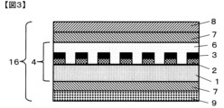
- FIG. 3 shows a schematic diagram of an example of the configuration of an internal diffuse reflectance evaluation substrate for evaluating the internal diffuse reflectance of a wiring substrate.
- the wiring substrate 4 has a laminated pattern of an opaque wiring electrode 2 and a light-shielding layer 3 on a transparent substrate 1, and further has a transparent protective layer 6.
- An anti-reflection film 8 is attached to the light-shielding layer forming surface of the wiring substrate (here, on the transparent protective layer 6) via an adhesive layer 7, and a black film 9 is attached to the surface of the transparent substrate 1 opposite the light-shielding layer via an adhesive layer 7 to prepare an internal diffuse reflectance evaluation substrate 16 in which reflection at the wiring substrate-air interface is reduced.
- the wiring substrate is a transparent substrate and the laminated pattern of the light-shielding layer and the opaque wiring electrode has a light-shielding layer on the transparent substrate side
- an anti-reflection film is attached to the transparent substrate via a transparent adhesive layer
- a black film is attached to the transparent protective layer via an adhesive layer to reduce reflection at the interface between the wiring substrate and the air, to prepare a substrate for evaluating internal diffuse reflectance.
- the diffuse reflectance at wavelengths of 540, 550, 560, and 570 nm is measured using a colorimetric system or the like from the light-shielding layer forming side, that is, from the anti-reflection film 8 side in the case of the configuration shown in FIG. 3, and the average value is calculated to calculate the average value R1 of the internal diffuse reflectance.
- the diffuse reflectance is affected by the reflectance of the material forming the light-shielding layer itself, the line width, area, and uneven shape of the light-shielding layer. For example, when the area of the light-shielding layer is the same, the thinner the line width W, the closer the wiring substrate surface is to the diffusing surface, and the internal diffuse reflectance tends to be higher due to the uneven shape of the light-shielding layer.
- Examples of methods for making R1 0.03 to 0.11% include a method in which the ratio of the laminate pattern area to the area of the laminate pattern forming part (laminated pattern area/laminate pattern forming part area, hereinafter "occupancy rate") S, the laminate pattern line width W, and the light-shielding layer thickness T1 are set to the preferred ranges described later, and a method in which the light-shielding layer is formed from the positive-type photosensitive resin composition for forming a light-shielding layer of the present invention described later are formed.
- the method of forming the light-shielding layer from the positive-type photosensitive resin composition for forming a light-shielding layer of the present invention described later is preferred because there are fewer restrictions on the wiring pattern.
- the average internal diffuse reflectance R1 [%], the average internal diffuse reflectance R2 [%] at a wavelength of 540 to 570 nm of the laminate pattern non-forming portion, and the occupancy rate S satisfy the relationship of the following formula (1). 0.0 ⁇ ((R1 ⁇ W) ⁇ (R2 ⁇ (1 ⁇ S)))/S ⁇ 7.0 (1)
- the reflection and scattering of the wiring surface in the area ratio S (laminate pattern portion) and the reflection and scattering of the non-wiring surface in the area ratio (1-S) (non-laminate pattern portion) affect the diffuse reflectance.
- the diffuse reflectance is affected by the area and unevenness of the light-shielding layer.
- (R1 ⁇ W) in the above formula (1) is an index of diffuse reflectance in the laminated pattern forming portion excluding the influence of the line width.
- the reflection and scattering of the non-wiring surface in the area ratio (1-S) affects the diffuse reflectance.
- the average value R2 of the internal diffuse reflectance at wavelengths of 540 to 570 nm in the laminated pattern non-forming portion is an index of diffuse reflectance in a wavelength region with high visibility
- (R2 ⁇ (1-S)) in the above formula (1) is an index of diffuse reflectance of the non-wiring surface in the laminated pattern forming portion.
- the difference between them i.e., the diffuse reflection of the wiring surface in the laminate pattern forming portion
- the area ratio S the difference between them
- the diffuse reflection of the wiring surface per unit area was focused on.
- the average value R2 of the internal diffuse reflectance at a wavelength of 540 to 570 nm of the laminate pattern non-forming portion can be calculated in the same manner as the above-mentioned R1 for the laminate pattern non-forming portion.
- the value of ((R1 ⁇ W) ⁇ (R2 ⁇ (1 ⁇ S)))/S (hereinafter, sometimes referred to as “diffuse reflection per unit area”) is more preferably 6.0 or less.
- the opaque wiring electrode preferably has a light transmittance of 25% or less at a wavelength of 550 nm. It is also preferable that the opaque wiring electrode has light-shielding properties against the exposure light used in the method for forming a light-shielding layer described below. Specifically, the light transmittance at a wavelength of 365 nm is preferably 15% or less. By making the light transmittance at a wavelength of 365 nm 15% or less, the function as a mask is improved in the method for forming a light-shielding layer described below, and the desired light-shielding layer can be formed with greater ease of processing.
- the light transmittance of the opaque wiring electrode can be measured using a microsurface spectrophotometer (VSS 400: manufactured by Nippon Denshoku Industries Co., Ltd.) for a square opaque wiring electrode with a side length of 0.1 mm or more.
- Materials constituting the opaque wiring electrode include, for example, metals such as silver, gold, copper, platinum, lead, tin, nickel, aluminum, tungsten, molybdenum, chromium, titanium, indium, etc., and conductive materials such as alloys of these. Two or more of these may be used. Among these, silver, copper, etc. are preferred from the viewpoint of conductivity.
- the raw material used to form the opaque wiring electrode is preferably conductive particles containing the conductive material described above, and the shape of the particles is preferably spherical.
- the average particle size of the conductive particles is preferably 0.03 ⁇ m or more from the viewpoint of improving the dispersibility of the conductive particles.
- the average particle size of the conductive particles is preferably 1.0 ⁇ m or less from the viewpoint of making the edges of the pattern of the opaque wiring electrode sharp.
- the average particle size of the conductive particles can be obtained by observing the conductive particles at a magnification of 15,000 times using a scanning electron microscope (SEM) or a transmission electron microscope (TEM), measuring the major axis length of each of 100 randomly selected conductive particles, and calculating the number average value.
- SEM scanning electron microscope
- TEM transmission electron microscope
- the opaque wiring electrode may contain an organic component in addition to the aforementioned conductive material.
- the opaque wiring electrode may be formed, for example, from a cured product of a photosensitive conductive composition containing conductive particles, an alkali-soluble resin, and a photopolymerization initiator, in which case the opaque wiring electrode contains the photopolymerization initiator and/or its photodecomposition product.
- the photosensitive conductive composition may contain additives such as a heat curing agent and a leveling agent, as necessary.
- Examples of the pattern shape of the opaque wiring electrode include a mesh shape and a stripe shape.
- Examples of the mesh shape include a lattice shape whose unit shapes are triangles, squares, polygons, circles, etc., or a lattice shape consisting of a combination of these unit shapes.
- the mesh shape is preferred from the viewpoint of making the conductivity of the pattern uniform. It is more preferable that the opaque wiring electrode is a metal mesh made of the above-mentioned metal and has a mesh-like pattern. When the opaque wiring electrode has a mesh-like pattern, the occupancy rate S can be reduced by increasing the mesh pitch.
- the thickness T2 [ ⁇ m] of the opaque wiring electrode is preferably 0.1 or more, and more preferably 0.3 or more, from the viewpoint of improving electrical conductivity.
- the thickness T2 [ ⁇ m] of the opaque wiring electrode is preferably 10 or less, more preferably 5.0 or less, and even more preferably 3.0 or less, from the viewpoint of forming finer wiring.
- T2 can be measured using a stylus-type step gauge.
- the line width of the pattern of the opaque wiring electrode is preferably 1 ⁇ m or more, more preferably 1.5 ⁇ m or more, and even more preferably 2 ⁇ m or more, from the viewpoint of improving electrical conductivity.
- the line width of the pattern of the opaque wiring electrode is preferably 10 ⁇ m or less, more preferably 8 ⁇ m or less, from the viewpoint of further reducing the value of the internal diffuse reflectance R1 and further improving the design visibility, when the pattern shape is the same.
- the line width of the pattern of the opaque wiring electrode can be obtained by magnifying and observing the laminated pattern formation part using an optical microscope, measuring the line width of the opaque wiring electrode at three randomly selected locations, and calculating the average value.
- the wiring substrate of the present invention has a light-shielding layer that contains a resin and a coloring component.
- the resin is preferably an alkali-soluble resin.
- alkali-soluble resins include resins having hydroxyl groups and/or carboxyl groups. Among these, resins having phenolic hydroxyl groups are preferred.
- resins having phenolic hydroxyl groups include novolac resins such as phenol novolac resin and cresol novolac resin, polymers of monomers having phenolic hydroxyl groups, and copolymers of monomers having phenolic hydroxyl groups with styrene, acrylonitrile, acrylic monomers, etc. Two or more of these may be included.
- Coloring components include inorganic pigments, organic pigments, dyes, etc., with pigments being preferred due to their excellent weather resistance.
- Organic pigments include soluble azo pigments, insoluble azo pigments, metal complex azo pigments, phthalocyanine pigments, condensed polycyclic pigments, black organic pigments such as C.I. Pigment Black 31 and 32, purple organic pigments such as C.I. Pigment Violet 19, 23, 29, 30, 32, 36, 37, 38, 39, 40, and 50, red organic pigments such as C.I.
- Inorganic pigments include carbon black, graphite, metal nitride particles such as titanium nitride and zirconium nitride, pine soot, iron oxides such as black iron, hematite, goethite and magnetite, chromium, lead, and composites of these metals.
- metal nitride particles are preferred because of their high transparency to the exposure light.
- the coloring component preferably absorbs light at wavelengths of 540 to 570 nm, from the viewpoint of setting the average internal diffuse reflectance R1 in the aforementioned range.
- coloring components that absorb light at wavelengths of 540 to 570 nm include metal nitride particles, red organic pigments, purple organic pigments, and blue organic pigments. Two or more of these may be contained. Among these, when a high-pressure mercury lamp is used as the exposure light source when forming the light-shielding layer, metal nitride particles, red organic pigments, purple organic pigments, and blue organic pigments are preferred, and when an LED lamp (365 nm) is used, metal nitride particles, red organic pigments, and purple organic pigments are preferred.
- metal nitride particles and purple organic pigments which can further improve visibility after the light-shielding layer is formed while maintaining the photosensitivity when an LED lamp (365 nm) is used as the light source when forming the light-shielding layer.
- the coloring component more preferably further contains a red organic pigment.
- a red organic pigment By including a red organic pigment, it is possible to improve visibility after the light-shielding layer is formed while maintaining photosensitivity when an LED lamp (365 nm) is used as the light source during the formation of the light-shielding layer.
- the thickness T1 [ ⁇ m] of the light-shielding layer is preferably 0.2 to 2.0.
- T1 [ ⁇ m] 0.2 or more the increase in internal diffuse reflectance caused by the surface unevenness of the opaque wiring electrode can be further suppressed, and R1 can be easily adjusted within the aforementioned range.
- T1 [ ⁇ m] 2.0 or less the unevenness on the transparent substrate can be reduced, and the generation of air bubbles caused by the unevenness when laminating the transparent protective layer can be suppressed.
- T1 can be measured using a stylus-type step gauge.
- the line width of the light-shielding layer is preferably equal to the line width of the opaque wiring electrode described above. Therefore, from the viewpoint of improving electrical conductivity, the line width W [ ⁇ m] of the laminated pattern is preferably 1 or more, more preferably 1.5 or more, and even more preferably 2 or more. On the other hand, in the case of the same pattern shape, the line width W [ ⁇ m] of the laminated pattern is preferably 10 or less, more preferably 8 or less, from the viewpoint of further reducing the value of the internal diffuse reflectance R1 and further improving the design visibility.
- the line width W of the laminated pattern can be obtained by magnifying and observing the laminated pattern formation part with an optical microscope, measuring the line width of the laminated pattern at three randomly selected points, and calculating the average value.
- the method for manufacturing the wiring substrate of the present invention preferably includes a step of forming an opaque wiring electrode on the transparent substrate (hereinafter, may be referred to as an "opaque wiring electrode forming step") and a step of forming a light-shielding layer containing a resin and a coloring component on the surface on which the opaque wiring electrode is formed to form a laminated pattern (hereinafter, may be referred to as a "laminate pattern forming step").
- methods for forming the opaque wiring electrode include, for example, a method of forming a pattern by photolithography using the above-mentioned photosensitive conductive composition, a method of forming a pattern by screen printing, gravure printing, inkjet, etc. using a conductive composition, a method of forming a film of a metal, a metal composite, a composite of a metal and a metal compound, a metal alloy, etc., and forming it by photolithography using a resist, etc.
- the pattern formed from the photosensitive conductive composition exhibits conductivity by heat curing, it is preferable to heat cure it at 140 to 500°C.
- examples of the light-shielding layer forming process include a method of applying a positive-type photosensitive resin composition for forming a light-shielding layer of the second aspect of the present invention described later onto an opaque wiring electrode, exposing the positive-type photosensitive resin composition for forming a light-shielding layer coating film from the side opposite to the coating side using the opaque wiring electrode as a mask, and developing the film to pattern the positive-type photosensitive resin composition for forming a light-shielding layer, and a method of transferring a light-shielding layer onto an opaque wiring electrode using a light-shielding layer transfer film of the present invention described later, exposing the light-shielding layer from the side opposite to the transfer side using the opaque wiring electrode as a mask, and developing the light-shielding layer to pattern the light-shielding layer.
- the latter method using a light-shielding layer transfer film is preferred.
- a light-shielding layer that maintains its shape using a light-shielding layer transfer film, it is possible to suppress the film thickness of the non-opaque wiring electrode portion from increasing due to leveling of the light-shielding layer during film formation, which would otherwise increase the required exposure amount and development time.
- a laminated pattern can be formed.
- exposure light sources include mercury lamps, halogen lamps, xenon lamps, LED lamps (365 nm, 405 nm), semiconductor lasers, and KrF or ArF excimer lasers.
- the i-line (wavelength 365 nm) of a mercury lamp and LED lamps (365 nm, 405 nm) are preferred, with LED lamps (365 nm) being even more preferred due to their high output.
- the exposure light may be applied while the substrate is stationary, or may be applied while the substrate is transported over the light source in a direction in which the exposure light is applied to the surface opposite the surface on which the light-shielding layer is formed.
- the developer used for development is preferably one that does not inhibit the conductivity of the electrode pattern, and is preferably an alkaline developer.
- alkaline developers include those exemplified as developers in WO 2018/168325.
- the development method include a method in which the developer is sprayed onto the surface of the resin layer while the substrate is stationary or rotated, a method in which the resin layer is immersed in the developer, and a method in which ultrasonic waves are applied to the resin layer while the resin layer is immersed in the developer.
- the light-shielding layer pattern obtained by development may be subjected to a rinse treatment using a rinse liquid.
- the rinse liquid include those exemplified as rinse liquids in WO 2018/168325.
- the obtained wiring substrate may be further heated at 100 to 300°C. Heating increases the hardness of the resin layer, suppresses chipping or peeling due to contact with other members, and further improves adhesion to the substrate and wiring. Examples of heating methods include heating with an oven, inert oven, or hot plate, and heating with electromagnetic waves from an infrared heater, etc.
- the positive-type photosensitive resin composition for forming a light-shielding layer of the present invention can be preferably used to form a light-shielding layer in the wiring substrate of the first embodiment of the present invention described above, and by forming a light-shielding layer from such a positive-type photosensitive resin composition for forming a light-shielding layer, the average value R1 of the internal diffuse reflectance can be easily adjusted to the aforementioned range.
- the positive-type photosensitive resin composition for forming a light-shielding layer of the present invention contains (a) an alkali-soluble resin, (b) a quinone diazide compound, (c) metal nitride particles, and (d) a purple organic pigment.
- positive-type photosensitivity refers to the property that the light-irradiated portion dissolves in the developer, and the unirradiated portion does not dissolve in the developer.
- Examples of the alkali-soluble resin include those exemplified for the light-shielding layer in the wiring substrate of the first embodiment of the present invention.
- the alkali-soluble resin (a) a resin having a phenolic hydroxyl group is preferable, and hydrogen bonding between the phenolic hydroxyl group and the quinone diazide compound (b) can further suppress the occurrence of film loss and peeling during development in unexposed areas, making it harder to see the opaque wiring electrode pattern.
- examples of the resin having a phenolic hydroxyl group those described for the light-shielding layer in the wiring substrate of the first embodiment of the present invention can be used.
- the content of the alkali-soluble resin (a) in the solid content of the positive photosensitive resin composition for forming the light-shielding layer is preferably 45 to 65 mass%.
- Examples of the quinone diazide compound include those exemplified as quinone diazide compounds contained in the positive photosensitive composition in WO 2018/168325.
- the content of the quinone diazide compound in the solid content of the positive photosensitive resin composition is preferably 5 to 25 mass%.
- the positive-type photosensitive resin composition for forming a light-shielding layer of the present invention contains (c) metal nitride particles and (d) purple organic pigment that absorb light in the wavelength range of 540 to 570 nm, which has high visibility, and also absorbs visible light in the wavelength range of 570 to 640 nm. This makes it possible to improve the visibility of the design after the light-shielding layer is formed while maintaining the photosensitivity when an LED lamp (365 nm) is used as the light source during the formation of the light-shielding layer.
- Examples of (c) metal nitride particles and (d) purple organic pigment include those described for the light-shielding layer in the wiring substrate of the first embodiment of the present invention.
- the content of (c) metal nitride particles in the solid content of the positive photosensitive resin composition for forming a light-shielding layer is preferably 2.0% by volume or more, and more preferably 2.5% by volume or more, from the viewpoint of further improving the design visibility.
- the content of metal nitride particles is preferably 6.0% by volume or less, and more preferably 5.0% by volume or less, from the viewpoint of photosensitivity.
- the content of the purple organic pigment (d) in the solid content of the positive photosensitive resin composition for forming a light-shielding layer is preferably 1.0% by volume or more from the viewpoint of further improving the visibility of the design.
- the content of the purple organic pigment (d) is preferably 8.0% by volume or less from the viewpoint of photosensitivity.
- the positive-type photosensitive resin composition for forming a light-shielding layer of the present invention preferably further contains (e) a red organic pigment.
- the red organic pigment absorbs light in the wavelength range of 460 to 540 nm and also absorbs visible light in the wavelength range of 570 to 640 nm, and therefore can improve the design visibility of the light-shielding layer while maintaining the photosensitivity when an LED lamp (365 nm) is used as the light source during the formation of the light-shielding layer.
- the positive photosensitive resin composition for forming a light-shielding layer of the present invention contains (e) a red organic pigment
- the total content of (c) the metal nitride particles, (d) the purple organic pigment, and (e) the red organic pigment in the solid content of the positive photosensitive resin composition is preferably 5.0% by volume or more from the viewpoint of bringing the diffuse reflection per unit area into the aforementioned preferred range and further improving visibility.
- the total content of these is preferably 15.0% by volume or less.
- the positive-type photosensitive resin composition for forming a light-shielding layer of the present invention may contain, as necessary, a monomer having an unsaturated double bond, a photopolymerization initiator, a photoacid generator, a thermal acid generator, a sensitizer, an adhesion improver, a surfactant, a thermal curing agent, a polymerization inhibitor, a rust inhibitor, a softener, a leveling agent, and the like.
- the positive-type photosensitive resin composition for forming a light-shielding layer of the present invention can be obtained, for example, by mixing (a) an alkali-soluble resin, (b) a quinone diazide compound, (c) metal nitride particles, (d) a purple organic pigment, and other additives as necessary, and then dispersing the mixture using a dispersing machine or kneading machine.
- dispersing machines and kneading machines include a jet mill, a bead mill, a ball mill, and a planetary ball mill.
- the positive-type photosensitive resin composition for forming a light-shielding layer of the present invention can be preferably used in the light-shielding layer transfer film of the present invention, and such a light-shielding layer transfer film can be preferably used to form a light-shielding layer in the wiring substrate of the first embodiment of the present invention described above.
- the light-shielding layer transfer film of the present invention has a light-shielding layer formed from the positive-type photosensitive resin composition for forming a light-shielding layer according to the second embodiment of the present invention described above on a release film.
- the release film is preferably one that has a release layer on its surface.
- the release agent forming the release layer may be, for example, a non-silicone release agent or a silicone release agent.
- the non-silicone release agent include long-chain alkyl and fluorine-based release agents. Two or more of these may be used.
- non-silicone release agents are preferred because, even if the release agent transfers during transfer, they are less likely to cause phenomena such as developer repelling in the subsequent process, particularly the development process, and can form a fine pattern while suppressing in-plane unevenness.
- the thickness of the release layer is preferably 50 nm or more from the viewpoint of suppressing transfer unevenness during transfer. On the other hand, the thickness of the release layer is preferably 500 nm or less from the viewpoint of suppressing transfer of the release agent during transfer.
- the peeling strength of the release film is preferably 500 mN/20 mm or more from the viewpoint of suppressing repelling during the formation of the light-shielding layer.
- the peeling strength of the release film is preferably 5,000 mN/20 mm or less from the viewpoint of widening the process margin during the transfer of the light-shielding layer.
- the peeling strength of the release film refers to the peeling strength when Nitto Denko Corporation's acrylic adhesive tape "31B" is applied to the surface on which the release layer is formed using a 2 kg roller, and after leaving it to stand for 30 minutes, it is peeled off under the conditions of a peeling angle of 180° and a peeling speed of 0.3 m/min.
- Films used for the release film include, for example, films containing resins such as polyethylene terephthalate (PET), cycloolefin polymer, polycarbonate, polyimide, aramid, fluororesin, acrylic resin, and polyurethane resin. Two or more of these may be used. Among these, those that are transparent to the exposure light used in the aforementioned laminated pattern formation process are preferred, and films containing PET, cycloolefin polymer, and polycarbonate are preferred. By selecting a film that is transparent to the exposure light, exposure can be performed through the release film in the aforementioned laminated pattern formation process, and contamination of the photomask can be suppressed by placing a release film between the light-shielding layer and the photomask.
- resins such as polyethylene terephthalate (PET), cycloolefin polymer, polycarbonate, polyimide, aramid, fluororesin, acrylic resin, and polyurethane resin. Two or more of these may be used.
- the thickness of the release film is preferably 5 ⁇ m or more, and more preferably 10 ⁇ m or more, from the viewpoint of improving transport stability during the formation of the light-shielding layer and suppressing unevenness in the thickness of the light-shielding layer.
- the thickness of the release film is preferably 300 ⁇ m or less, and more preferably 200 ⁇ m or less, from the viewpoint of ease of handling during peeling.
- the thickness T1' [ ⁇ m] of the light-shielding layer of the light-shielding layer transfer film is preferably 0.3 or more, more preferably 0.5 or more, from the viewpoint of making the opaque wiring electrode less visible.
- the thickness T1' [ ⁇ m] of the light-shielding layer is preferably 2.0 or less, from the viewpoint of reducing the development time and further improving processability. Note that T1' can be measured using a stylus-type step gauge.
- the thickness T1' of the light-shielding layer corresponds to the thickness T1, but may vary depending on the method of forming the light-shielding layer.
- the light-shielding layer transfer film of the present invention can be obtained, for example, by applying a positive-type photosensitive resin composition for forming a light-shielding layer onto a release film.
- Methods for applying the positive photosensitive resin composition for forming a light-shielding layer onto a release film include, for example, spin coating using a spinner, spray coating, roll coating, screen printing, or coating using a slit coater, blade coater, die coater, calendar coater, meniscus coater, or bar coater.
- the coating thickness of the positive photosensitive resin composition for forming a light-shielding layer is preferably set so that the thickness T1 of the light-shielding layer falls within the preferred range described above.
- the positive-type photosensitive resin composition for forming the light-shielding layer contains a solvent
- the drying temperature is preferably 60 to 120°C, and the drying time is preferably 1 to 20 minutes.
- the heating and drying device for example, an oven, a hot plate, etc. are preferable.
- Phenol novolac resin WR-104 (manufactured by DIC Corporation).
- the acid value of the resulting acrylic resin having a carboxy group was measured in accordance with JIS K 0070 (1992) to find that it was 103 mgKOH/g.
- the weight average molecular weight of the resulting acrylic resin having a carboxy group was 17,000.
- the mixture was heated and stirred at 80°C for another 6 hours to carry out a polymerization reaction. Thereafter, 1 g of hydroquinone monomethyl ether was added to terminate the polymerization reaction.
- the acid value was measured in the same manner as in Production Example 2 and found to be 153 mgKOH/g.
- the weight average molecular weight of the resulting acrylic resin having a phenolic hydroxyl group and a carboxyl group was 10,000.
- CM-2500d a spectrophotometer manufactured by Konica Minolta Sensing Co., Ltd.
- the diffuse reflectance SCE at wavelengths of 540, 550, 560, and 570 nm of the laminated pattern-formed portion of the internal diffuse reflectance evaluation substrate was measured, and the average value was taken as the average internal reflectance R1.
- the diffuse reflectance SCE was measured at wavelengths of 540, 550, 560, and 570 nm of the non-layer pattern forming portion of the substrate for evaluating internal diffuse reflectance using a spectrophotometer (CM-2500d) manufactured by Konica Minolta Sensing Co., Ltd., and the average value was taken as the average internal reflectance R2.
- Example 1 ⁇ Opaque Wiring Electrode Forming Process>
- AN Wizus registered trademark
- the photosensitive conductive paste (D-1) obtained in Production Example 4 was applied by spin coating so that the thickness after drying was 1 ⁇ m, and dried at 90 ° C. for 8 minutes.
- an exposure device (PEM-6M; manufactured by Union Optical Co., Ltd.) was used to expose at an exposure dose of 150 mJ / cm 2 (converted to a wavelength of 365 nm).
- the mesh-shaped pattern is a negative pattern having a mesh pitch 14 of 400 ⁇ m and a mesh angle 15 of 58 °, and an opening width of 4 ⁇ m, a laminated pattern portion (mask opening) 12, and a non-laminated pattern portion (mask light shielding portion) 13.
- black and white are inverted for convenience of illustration.
- the obtained positive photosensitive resin composition 1 for forming a light-shielding layer was spin-coated on the opaque wiring electrode surface formed in the ⁇ Opaque wiring electrode forming step> so that the film thickness after drying was 1.4 ⁇ m, and dried at 100 ° C. for 10 minutes.
- an exposure device (PEM-6M) was used to expose from the opposite side of the opaque wiring electrode forming surface under the condition of an exposure amount (converted to a wavelength of 365 nm) of 10,000 mJ / cm 2 , and development was performed using a 2.38 mass% tetramethylammonium hydroxide aqueous solution as a developer until the transparent substrate of the exposed portion was exposed, forming a light-shielding layer pattern on the opaque wiring electrode, and forming a laminated pattern. Furthermore, it was heated in a box oven at 220 ° C. for 60 minutes.
- the photosensitive insulating paste obtained in (Production Example 5) was spin-coated so that the film thickness after drying was 3.0 ⁇ m, and dried at 80 ° C. for 5 minutes.
- an exposure device PEM-6M
- the coated surface was exposed under the condition of an exposure amount (converted to a wavelength of 365 nm) of 100 mJ / cm 2 , and development was performed for 60 seconds using a 0.1 mass % tetramethylammonium hydroxide aqueous solution as a developer. Furthermore, it was heated in a box oven at 220 ° C. for 60 minutes to obtain a wiring substrate on which a transparent protective layer was formed.
- Example 2 A wiring substrate was obtained in the same manner as in Example 1, except that the mesh pitch and occupancy rate S of the exposure mask in the ⁇ Opaque wiring electrode formation process> and the composition in (Preparation of positive-type photosensitive resin composition for forming light-shielding layer) were changed as shown in Table 1.
- Examples 3 to 9 A wiring substrate was obtained in the same manner as in (Example 2), except that the composition in (Preparation of positive-type photosensitive resin composition for forming light-shielding layer) and the exposure dose in (Formation of light-shielding layer) were changed as shown in Tables 1 and 2.
- Example 1 A wiring substrate was obtained in the same manner as in Example 3, except that (formation of a light-shielding layer) was not carried out.
- Example 6 A wiring substrate was obtained in the same manner as in Example 2, except that the composition in (Preparation of positive-type photosensitive resin composition for forming light-shielding layer) and the exposure dose in (Formation of light-shielding layer) were changed as shown in Table 3.
- Example 10 ⁇ Formation of Opaque Wiring Electrodes> In the same manner as in Example 2, a substrate with an opaque wiring electrode was obtained.
- a non-silicone release agent AL-5 (manufactured by Lintec Corporation) was applied to one side of a PET film "Lumirror (registered trademark)" FB40 (manufactured by Toray Industries, Inc.) (thickness: 16 ⁇ m), and the film was heat-treated and dried to form a release layer having a thickness of 100 nm on the surface of the substrate, thereby obtaining a release film.
- an acrylic adhesive tape "31B” manufactured by Nitto Denko Corporation was attached to the release layer-formed surface using a 2 kg roller, and the film was allowed to stand for 30 minutes. After that, the peel force was measured when the film was peeled off under the conditions of a peel angle of 180° and a peel speed of 0.3 m/min, and was found to be 1,480 mN/20 mm.
- the positive-type photosensitive resin composition 2 for forming a light-shielding layer was applied to the release layer surface of the obtained release film using a coater so that the thickness after drying T1' was 1.4 ⁇ m, and the film was dried at 80° C. for 4 minutes to form a light-shielding layer, thereby obtaining a light-shielding layer transfer film.
- the light-shielding layer transfer film obtained by ⁇ Preparation of light-shielding layer transfer film> was thermocompressed at 80°C and a speed of 0.1 m/min so that the light-shielding layer of the light-shielding layer transfer film obtained by ⁇ Preparation of light-shielding layer transfer film> was in contact with the opaque wiring electrode formed in the ⁇ Opaque wiring electrode formation process>, and the release film was peeled off.
- the film was exposed from the opposite side of the opaque wiring electrode formation surface under the condition of an exposure amount (converted to a wavelength of 365 nm) of 100 mJ/cm 2 using an exposure device (PEM-6M), and development was performed using a 1.00 mass% sodium carbonate aqueous solution as a developer until the transparent substrate of the exposed portion was exposed, forming a light-shielding layer pattern on the opaque wiring electrode, and forming a laminated pattern. Further, the film was heated in a box oven at 220°C for 60 minutes.
- a transparent protective layer was formed in the same manner as in Example 1 to obtain a wiring substrate.
Landscapes
- Engineering & Computer Science (AREA)
- Physics & Mathematics (AREA)
- General Physics & Mathematics (AREA)
- Theoretical Computer Science (AREA)
- General Engineering & Computer Science (AREA)
- Human Computer Interaction (AREA)
- Manufacturing & Machinery (AREA)
- Microelectronics & Electronic Packaging (AREA)
- Power Engineering (AREA)
- Spectroscopy & Molecular Physics (AREA)
- Optical Filters (AREA)
- Materials For Photolithography (AREA)
Priority Applications (2)
| Application Number | Priority Date | Filing Date | Title |
|---|---|---|---|
| JP2023566497A JPWO2024135082A1 (https=) | 2022-12-20 | 2023-10-25 | |
| CN202380065843.7A CN119895367A (zh) | 2022-12-20 | 2023-10-25 | 布线基板、遮光层形成用正型感光性树脂组合物、遮光层转印膜及布线基板的制造方法 |
Applications Claiming Priority (2)
| Application Number | Priority Date | Filing Date | Title |
|---|---|---|---|
| JP2022-202949 | 2022-12-20 | ||
| JP2022202949 | 2022-12-20 |
Publications (1)
| Publication Number | Publication Date |
|---|---|
| WO2024135082A1 true WO2024135082A1 (ja) | 2024-06-27 |
Family
ID=91588557
Family Applications (1)
| Application Number | Title | Priority Date | Filing Date |
|---|---|---|---|
| PCT/JP2023/038439 Ceased WO2024135082A1 (ja) | 2022-12-20 | 2023-10-25 | 配線基板、遮光層形成用ポジ型感光性樹脂組成物、遮光層転写フィルムおよび配線基板の製造方法 |
Country Status (3)
| Country | Link |
|---|---|
| JP (1) | JPWO2024135082A1 (https=) |
| CN (1) | CN119895367A (https=) |
| WO (1) | WO2024135082A1 (https=) |
Citations (5)
| Publication number | Priority date | Publication date | Assignee | Title |
|---|---|---|---|---|
| JP2014197183A (ja) * | 2013-03-06 | 2014-10-16 | 日東電工株式会社 | 画像表示装置 |
| JP2015184958A (ja) * | 2014-03-25 | 2015-10-22 | 富士フイルム株式会社 | タッチパネルモジュールおよび電子機器 |
| WO2020040054A1 (ja) * | 2018-08-23 | 2020-02-27 | 富士フイルム株式会社 | 転写フィルム、積層体、及びパターン形成方法 |
| WO2022130803A1 (ja) * | 2020-12-15 | 2022-06-23 | 東レ株式会社 | 配線基板 |
| JP2022112699A (ja) * | 2021-01-22 | 2022-08-03 | 東レ株式会社 | 着色樹脂組成物、遮光膜、加飾基板及び加飾フィルム |
Family Cites Families (5)
| Publication number | Priority date | Publication date | Assignee | Title |
|---|---|---|---|---|
| JP2017202631A (ja) * | 2016-05-12 | 2017-11-16 | 東レ株式会社 | 転写フィルム、積層基材、カバーガラス、積層基材の製造方法 |
| JP7517149B2 (ja) * | 2019-03-14 | 2024-07-17 | 東レ株式会社 | 感光性樹脂組成物、感光性樹脂シート、硬化膜、硬化膜の製造方法、有機el表示装置、および電子部品 |
| KR102624811B1 (ko) * | 2020-01-21 | 2024-01-16 | 도레이 카부시키가이샤 | 포지티브형 감광성 수지 조성물, 경화막, 적층체, 도전 패턴이 형성된 기판, 적층체의 제조 방법, 터치 패널 및 유기 el 표시 장치 |
| KR102819502B1 (ko) * | 2020-03-30 | 2025-06-12 | 도레이 카부시키가이샤 | 수지 조성물, 차광막, 및 격벽이 형성된 기판 |
| WO2021199996A1 (ja) * | 2020-03-30 | 2021-10-07 | 富士フイルム株式会社 | 感光性転写材料、樹脂パターンの製造方法、回路配線の製造方法、及び感光性転写材料用仮支持体 |
-
2023
- 2023-10-25 CN CN202380065843.7A patent/CN119895367A/zh active Pending
- 2023-10-25 WO PCT/JP2023/038439 patent/WO2024135082A1/ja not_active Ceased
- 2023-10-25 JP JP2023566497A patent/JPWO2024135082A1/ja active Pending
Patent Citations (5)
| Publication number | Priority date | Publication date | Assignee | Title |
|---|---|---|---|---|
| JP2014197183A (ja) * | 2013-03-06 | 2014-10-16 | 日東電工株式会社 | 画像表示装置 |
| JP2015184958A (ja) * | 2014-03-25 | 2015-10-22 | 富士フイルム株式会社 | タッチパネルモジュールおよび電子機器 |
| WO2020040054A1 (ja) * | 2018-08-23 | 2020-02-27 | 富士フイルム株式会社 | 転写フィルム、積層体、及びパターン形成方法 |
| WO2022130803A1 (ja) * | 2020-12-15 | 2022-06-23 | 東レ株式会社 | 配線基板 |
| JP2022112699A (ja) * | 2021-01-22 | 2022-08-03 | 東レ株式会社 | 着色樹脂組成物、遮光膜、加飾基板及び加飾フィルム |
Also Published As
| Publication number | Publication date |
|---|---|
| JPWO2024135082A1 (https=) | 2024-06-27 |
| CN119895367A (zh) | 2025-04-25 |
Similar Documents
| Publication | Publication Date | Title |
|---|---|---|
| CN107109131B (zh) | 触摸面板电极保护膜形成用组合物及其应用 | |
| JP2004126600A (ja) | 溶解特性を調節する感光性樹脂組成物及びこれを用いた二層構造パターンの形成方法 | |
| TWI733001B (zh) | 附有配線電極之基板的製造方法 | |
| JP7081696B2 (ja) | ポジ型感光性樹脂組成物、硬化膜、積層体、導電パターン付き基板、積層体の製造方法、タッチパネル及び有機el表示装置 | |
| JP7035437B2 (ja) | 導電パターン付き基板の製造方法および導電パターン付き基板 | |
| WO2024135082A1 (ja) | 配線基板、遮光層形成用ポジ型感光性樹脂組成物、遮光層転写フィルムおよび配線基板の製造方法 | |
| JP4348226B2 (ja) | 金属化合物微粒子及びこれを用いた遮光膜 | |
| JP5252919B2 (ja) | 感光性転写材料 | |
| JP7472601B2 (ja) | 配線電極付き基板の製造方法 | |
| JP7729208B2 (ja) | 配線基板 | |
| WO2024190033A1 (ja) | 配線付き基材およびその製造方法 | |
| JP2024061122A (ja) | 配線付き基材の製造方法 | |
| WO2024004318A1 (ja) | 配線電極付き基板の製造方法 | |
| CN101263424B (zh) | 光敏组合物、转印材料、遮光膜及其制备方法、显示装置用滤色器、显示装置用衬底和显示装置 | |
| WO2021193354A1 (ja) | 樹脂組成物、配線基板及び導電性パターンの製造方法 | |
| JP7322753B2 (ja) | 感光性樹脂組成物、遮光層及びタッチセンサーパネル | |
| JPWO2019065234A1 (ja) | 電極付き基板の製造方法 | |
| JP2023123957A (ja) | 感光性樹脂組成物、配線基板および配線基板の製造方法 | |
| JP2006337485A (ja) | カラーフィルター,液晶表示素子、及び液晶表示装置 | |
| JPWO2020110453A1 (ja) | 積層部材 | |
| CN116602061A (zh) | 布线基板 | |
| JPWO2000058788A1 (ja) | 高解像度な光重合性積層体並びにこれを用いた半導体装置 | |
| JP2003315530A (ja) | 液晶表示装置用カラーフィルターおよびこれを用いた半透過型液晶表示装置 | |
| JP2008175934A (ja) | フォトマスクおよびカラーフィルター基板の製造方法 |
Legal Events
| Date | Code | Title | Description |
|---|---|---|---|
| WWE | Wipo information: entry into national phase |
Ref document number: 2023566497 Country of ref document: JP |
|
| 121 | Ep: the epo has been informed by wipo that ep was designated in this application |
Ref document number: 23906457 Country of ref document: EP Kind code of ref document: A1 |
|
| WWE | Wipo information: entry into national phase |
Ref document number: 202380065843.7 Country of ref document: CN |
|
| WWP | Wipo information: published in national office |
Ref document number: 202380065843.7 Country of ref document: CN |
|
| NENP | Non-entry into the national phase |
Ref country code: DE |
|
| 122 | Ep: pct application non-entry in european phase |
Ref document number: 23906457 Country of ref document: EP Kind code of ref document: A1 |