WO2024048713A1 - 印刷配線板及びその製造方法 - Google Patents
印刷配線板及びその製造方法 Download PDFInfo
- Publication number
- WO2024048713A1 WO2024048713A1 PCT/JP2023/031794 JP2023031794W WO2024048713A1 WO 2024048713 A1 WO2024048713 A1 WO 2024048713A1 JP 2023031794 W JP2023031794 W JP 2023031794W WO 2024048713 A1 WO2024048713 A1 WO 2024048713A1
- Authority
- WO
- WIPO (PCT)
- Prior art keywords
- layer
- hole
- conductor
- opening
- printed wiring
- Prior art date
- Legal status (The legal status is an assumption and is not a legal conclusion. Google has not performed a legal analysis and makes no representation as to the accuracy of the status listed.)
- Ceased
Links
Images




Classifications
-
- H—ELECTRICITY
- H05—ELECTRIC TECHNIQUES NOT OTHERWISE PROVIDED FOR
- H05K—PRINTED CIRCUITS; CASINGS OR CONSTRUCTIONAL DETAILS OF ELECTRIC APPARATUS; MANUFACTURE OF ASSEMBLAGES OF ELECTRICAL COMPONENTS
- H05K3/00—Apparatus or processes for manufacturing printed circuits
- H05K3/40—Forming printed elements for providing electric connections to or between printed circuits
- H05K3/42—Plated through-holes or plated via connections
- H05K3/421—Blind plated via connections
-
- H—ELECTRICITY
- H05—ELECTRIC TECHNIQUES NOT OTHERWISE PROVIDED FOR
- H05K—PRINTED CIRCUITS; CASINGS OR CONSTRUCTIONAL DETAILS OF ELECTRIC APPARATUS; MANUFACTURE OF ASSEMBLAGES OF ELECTRICAL COMPONENTS
- H05K2201/00—Indexing scheme relating to printed circuits covered by H05K1/00
- H05K2201/20—Details of printed circuits not provided for in H05K2201/01 - H05K2201/10
- H05K2201/2072—Anchoring, i.e. one structure gripping into another
-
- H—ELECTRICITY
- H05—ELECTRIC TECHNIQUES NOT OTHERWISE PROVIDED FOR
- H05K—PRINTED CIRCUITS; CASINGS OR CONSTRUCTIONAL DETAILS OF ELECTRIC APPARATUS; MANUFACTURE OF ASSEMBLAGES OF ELECTRICAL COMPONENTS
- H05K3/00—Apparatus or processes for manufacturing printed circuits
- H05K3/46—Manufacturing multilayer circuits
- H05K3/4644—Manufacturing multilayer circuits by building the multilayer layer by layer, i.e. build-up multilayer circuits
Definitions
- the present disclosure relates to a printed wiring board and a method for manufacturing the same.
- a printed wiring board in which a build-up layer is laminated on at least one surface of a core substrate has been disclosed (for example, Patent Document 1).
- Via conductors are provided in the buildup layer. This via conductor is connected to the plated wiring on the surface of the core substrate and the plated wiring on the surface of the buildup layer. These plated wirings are electrically connected by via conductors.
- One aspect of the present disclosure is core board, a build-up layer laminated on the core substrate,
- the buildup layer is an insulating layer laminated on the core substrate; a hole penetrating the insulating layer in the thickness direction; a via conductor filled in the hole; has
- the printed wiring board has the via conductor having a cylindrical shape.
- One aspect of the present disclosure is preparing a laminate in which a build-up precursor layer comprising an insulating layer and a metal underlayer in this order is stacked on a core substrate; A first mask having a first through hole is disposed above the base layer side of the laminate, and a first laser beam is irradiated toward the base layer through the first through hole to remove the base layer. forming an opening in the A second mask having a second through hole smaller in diameter than the first through hole is disposed above the first through hole in the base layer, and a second laser beam is directed to the insulating layer through the opening.
- a method of manufacturing a printed wiring board including:
- the via conductor is difficult to come out of the insulating layer.
- FIG. 1 shows a cross section of a printed wiring board.
- FIG. 2 shows an enlarged view of region II in FIG.
- FIG. 3 shows an enlarged cross-section of the boundary between the outer periphery of the via conductor and the inner periphery of the hole.
- FIG. 4 shows an enlarged cross-section of the boundary between the outer periphery of the via conductor and the inner periphery of the hole.
- FIG. 5 shows an enlarged cross section of a via conductor in a modified example.
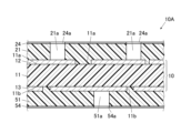
- FIG. 6 shows a cross section of a laminate in one step of manufacturing a printed wiring board.
- FIG. 7 shows a cross section of the laminate in a step after the step of FIG. 6.
- FIG. 8 shows a cross section of the laminate in a step after the step of FIG. 7.
- FIG. 1 shows a cross section of a printed wiring board.
- FIG. 2 shows an enlarged view of region II in FIG.
- FIG. 3 shows an enlarged cross-section of the boundary between the outer
- FIG. 9 shows a cross section of the laminate in a step after the step of FIG. 8.
- FIG. 10 shows a cross section of the laminate in a step after the step of FIG. 9.
- FIG. 11 shows a cross section of the laminate in a step after the step of FIG. 10.
- FIG. 12 shows a cross section of the laminate in a step after the step of FIG. 11.
- FIG. 13 shows a cross section of the laminate in a step after the step of FIG. 12.
- the printed wiring board 1 of the present disclosure may include any constituent members not shown in the drawings. Further, the dimensions of the members in the drawings do not faithfully represent the dimensions and dimensional ratios of the actual constituent members.
- Printed wiring board 1 is a multilayer board.
- Printed wiring board 1 has a core substrate 10 and a first buildup layer 20.
- this printed wiring board 1 is provided with the 1st solder resist layer 40, the 2nd buildup layer 50, and the 2nd solder resist layer 70 as shown in FIG. 1 as needed.
- the second solder resist layer 70, the second buildup layer 50, the core substrate 10, the first buildup layer 20, and the first solder resist layer 40 may be stacked in this order.
- the core substrate 10 has a base material 11 and conductor layers 12 and 13.
- the base material 11 has a flat plate shape.
- the base material 11 has a first surface 11a and a second surface 11b opposite to the first surface 11a.
- the first surface 11a and the second surface 11b face oppositely to each other.
- the base material 11 has a thickness from the first surface 11a to the second surface 11b.
- the direction from the first surface 11a to the second surface 11b and the opposite direction are the thickness directions.
- the base material 11 is made of an insulating material.
- insulating materials include organic resins such as epoxy resins, bismaleimide-triazine resins, polyimide resins, polyphenylene ether (PPE) resins, polyphenylene oxide (PPO) resins, cyanate ester resins, and liquid crystal polymers. can be mentioned. Two or more types of these organic resins may be mixed. A reinforcing material may be blended with one or more of these organic resins. Examples of the reinforcing material include cloth materials such as glass fiber, glass nonwoven fabric, aramid fiber, aramid nonwoven fabric, polyester fiber, and polyester nonwoven fabric. One or more of these organic resins may contain inorganic fillers such as barium sulfate, talc, clay, glass, calcium carbonate, titanium, and the like.
- the conductor layer 12 is laminated on the first surface 11a of the base material 11.
- the conductor layer 13 is laminated on the second surface 11b of the base material 11.
- the conductor layers 12 and 13 are formed into a wiring pattern.
- the material of the conductor layers 12 and 13 is, for example, a conductive metal such as copper.
- the conductor layers 12 and 13 are made of metal plating such as copper plating, for example.
- the thickness of the conductor layers 12 and 13 is preferably 18 ⁇ m or more and 100 ⁇ m or less, for example.
- the core substrate 10 may have a multilayer structure.
- the multilayer structure include the following embodiments.
- a multilayer structure has multiple insulating layers, one or more inner conductor layers and two surface conductor layers.
- the insulating layers are laminated in order.
- An inner conductor layer is sandwiched between these insulating layers.
- the two surface conductor layers are laminated on the two outermost surfaces of a laminate made of a plurality of insulating layers, in the same way that the conductor layers 12 and 13 are laminated on the surfaces 11a and 11b of the base material 11, respectively.
- the inner conductor layer and the surface conductor layer form a wiring pattern.
- the first buildup layer 20 has an insulating layer 21 , at least one via conductor 22 and a surface conductor layer 23 .
- the insulating layer 21 is laminated on the surface of the core substrate 10. That is, the insulating layer 21 covers the conductor layer 12 and also covers the first surface 11a of the base material 11. In other words, the core substrate 10 has the conductor layer 12 on the surface in contact with the buildup layer 20.
- the thickness of the insulating layer 21 is, in other words, from the surface 12d of the conductor layer 12 on the opposite side to the surface 12c in contact with the first surface 11a with respect to the conductor layer 12, to the surface of the insulating layer 21 on the opposite side to the core substrate 10 with respect to the insulating layer 21.
- the thickness up to 21d is, for example, 40 to 100 ⁇ m.
- the insulating layer 21 is made of an insulating material.
- insulating materials include epoxy resin, bismaleimide-triazine resin, polyimide resin, polyphenylene ether (PPE) resin, polyphenylene oxide (PPO) resin, cyanate ester resin, and polytetrafluoroethylene (PTFE) resin. and organic resins such as liquid crystal polymers. Two or more types of these organic resins may be mixed. A reinforcing material may be blended with one or more of these organic resins. Examples of the reinforcing material include cloth materials such as glass fiber, glass nonwoven fabric, aramid fiber, aramid nonwoven fabric, polyester fiber, and polyester nonwoven fabric. One or more of these organic resins may contain inorganic fillers such as barium sulfate, talc, clay, glass, calcium carbonate, titanium, and the like.
- the via conductor 22 penetrates the insulating layer 21 in the thickness direction.
- the insulating layer 21 has at least one hole 21a penetrating the insulating layer 21 in the thickness direction, and the via conductor 22 is filled in each hole 21a.
- the material of the via conductor 22 is, for example, a conductive metal such as copper.
- the via conductor 22 is coupled to the conductor layer 12 of the core substrate 10 and is electrically connected to the conductor layer 12 .
- the buildup layer 20 may have a base layer 24 between the insulating layer 21 and the upper layer 25.
- the base layer 24 is preferably electrically conductive.
- the base layer 24 is preferably a metal film.
- FIG. 2 is an enlarged view of region II in FIG. 1.
- the surface 12a of the portion of the conductor layer 12 that is in contact with the via conductor 22 may have a concave shape.
- the bottom 22a of the via conductor 22 will fit into the recess.
- the contact area between conductor layer 12 and via conductor 22 becomes larger. This makes it possible to increase the bonding force between the conductor layer 12 and the via conductor 22.
- the end surface of the via conductor 22 on the conductor layer 12 side has a convex shape. In this way, the bottom 22a of the via conductor 22 is fitted into the concave surface 12a.
- the via conductor 22 is shaped like a cylinder around a central axis along the thickness direction of the insulating layer 21.
- the term cylindrical means that the diameter of the via conductor 22 is uniform over the thickness direction.
- the via conductor 22 is in contact with the inner wall surface of the hole 21a throughout its thickness.
- the inner wall surface of the hole 21a has an uneven shape, and the via conductor 22 is filled up to the unevenness of the inner wall surface of the hole 21a throughout the thickness direction.
- the via conductor 22 is formed in an uneven manner, and the unevenness of the via conductor 22 meshes with the unevenness of the inner wall surface of the hole 21a without any gaps.
- FIGS. 3 and 4 are enlarged cross-sectional views of the boundary between the via conductor 22 and the inner wall surface of the hole 21a.
- the portion shown in FIG. 4 is in a different position than the portion shown in FIG.
- the unevenness of the via conductor 22 has at least one convex portion 22b and at least one convex portion 22c.
- the protrusions 22b and 22c protrude radially outward and pierce the insulating layer 21.
- the convex portions 22b and 22c protrude radially outward.
- the convex portions 22b and 22c are arranged so as to pierce the insulating layer 21. In this case, the convex portion 22b is oriented toward the surface conductor layer 23.
- the convex portion 22b is oriented toward the upper layer 25.
- the convex portion 22b is oriented diagonally from the side surface of the via conductor 22, and is oriented toward the surface conductor layer 23 or the upper layer 25.
- the convex portion 22c is oriented toward the core substrate 10. In other words, the convex portion 22c is oriented diagonally from the side surface of the via conductor 22, and is oriented toward the core substrate 10.
- the surface conductor layer 23 is laminated on the surface 21d of the insulating layer 21 on the side opposite to the core substrate 10 with respect to the insulating layer 21.
- the surface conductor layer 23 forms a wiring pattern.
- the surface conductor layer 23 is electrically connected to the via conductor 22.
- the surface conductor layer 23 may have a base layer 24 and an upper layer 25.
- the upper layer 25 is a metal film located on the opposite side of the insulating layer 21 with the base layer 24 in the surface conductor layer 23 .
- the upper layer 25 is a part of the metal film that constitutes the surface conductor layer 23.
- the base layer 24 and the upper layer 25 are arranged to be laminated in this order on the surface 21d of the insulating layer 21 on the opposite side of the core substrate 10 with respect to the insulating layer 21.
- the thickness of the base layer 24 is, for example, 2 ⁇ m or more and 17 ⁇ m or less.
- the base layer 24 and the upper layer 25 form a wiring pattern.
- the material of the base layer 24 and the upper layer 25 is, for example, a conductive metal such as copper.
- the base layer 24 has an opening 24a at a position overlapping the hole 21a.
- the inner edge of the opening 24a is located at a position that overlaps with the opening edge of the hole 21a or outside the opening edge of the hole 21a.
- the base layer 24 has a tapered portion 24b around the opening 24a.
- the periphery of the opening 24a refers to an area that includes the inner edge (or edge) of the opening 24a and extends from the inner edge by a predetermined width in the normal direction.
- the thickness of the tapered portion 24b gradually decreases toward the edge of the opening 24a. In other words, it is preferable that the thickness of the base layer 24 increases in the direction of the normal line outward from the edge of the opening 24a.
- the vicinity of the tapered portion 24b of the base layer 24 is a region where a plurality of members such as the insulating layer 21, the via conductor 22, and the upper layer 25 are in contact with each other. Stress is likely to occur in areas where multiple members are in contact with each other due to differences in coefficient of thermal expansion and Young's modulus of each member.
- the base layer 24 has a shape in which the thickness increases from the edge of the opening 24a toward the outside in the direction of the normal line, cracks may occur near the edge of the opening 24a, which is the end of the tapered portion 24b. Easy stress can be reduced.
- the thickness of the base layer 24 becomes thinner toward the edge of the opening 24a.
- the surface of the tapered portion 24b in contact with the upper layer 25 has a curved shape convex toward the upper layer 25 side.
- the upper layer 25 is connected to the via conductor 22 through the opening 24a, and the via conductor 22 is integral with the upper layer 25.
- the thickness of the portion of the upper layer 25 where the tapered portion 24b overlaps gradually decreases toward the edge of the opening 24a.
- the angle ⁇ of the tapered portion 24b at the edge of the opening 24a is, for example, more than 45°, and more specifically preferably 50° or more and 80° or less.
- the portion of the surface conductor layer 23 that overlaps with the via conductor 22 is a land having a diameter longer than the line width of the wiring pattern.
- the diameter of the land is preferably 200 ⁇ m or more and 250 ⁇ m or less, for example.
- the printed wiring board 1 may have the second buildup layer 50.
- the second buildup layer 50 is located on the surface of the core substrate 10 opposite to the surface on which the first buildup layer 20 is located.
- Core substrate 10 may have conductor layer 13 on the surface in contact with second buildup layer 50 .
- the second buildup layer 50 has an insulating layer 51, at least one via conductor 52, and a surface conductor layer 53.
- the second buildup layer 50 is provided similarly to the first buildup layer 20.
- the insulating layer 51 of the second buildup layer 50 corresponds to the insulating layer 21 of the first buildup layer 20, and the via conductor 52 of the second buildup layer 50 corresponds to the via conductor 22 of the first buildup layer 20.
- the surface conductor layer 53 of the second buildup layer 50 corresponds to the surface conductor layer 23 of the first buildup layer 20.
- the hole 51a of the insulating layer 51 corresponds to the hole 21a of the insulating layer 21
- the base layer 54 of the surface conductor layer 53 corresponds to the base layer 24 of the surface conductor layer 23
- the upper layer 55 of the surface conductor layer 53 corresponds to the base layer 24 of the surface conductor layer 23.
- the opening 54 a of the base layer 54 corresponds to the opening 24 a of the base layer 24 .
- the base layer 54 has a tapered part around the opening whose thickness gradually decreases toward the edge of the opening 54a.
- solder resist layer The solder resist layers 40 and 70 are laminated on both sides of the laminate of the first buildup layer 20, core substrate 10, and second buildup layer 50, respectively. That is, the first solder resist layer 40 covers the surface conductor layer 23 and also covers the surface 21 d of the insulating layer 21 on the side opposite to the core substrate 10 with respect to the insulating layer 21 .
- the second solder resist layer 70 covers the surface conductor layer 53 and also covers the surface 51 d of the insulating layer 51 on the side opposite to the core substrate 10 with respect to the insulating layer 51 .
- the first solder resist layer 40 has at least one opening 41. A portion of the surface conductor layer 23 overlaps the opening 41, and the portion of the surface conductor layer 23 inside the opening 41 is a terminal. Like the first solder resist layer 40, the second solder resist layer 70 also has at least one opening 71. A portion of the surface conductor layer 53 overlaps the opening 71, and the portion of the surface conductor layer 53 inside the opening 71 is a terminal.
- the number of first buildup layers 20 is one.
- a plurality of first buildup layers 20 may be stacked between the core substrate 10 and the first solder resist layer 40.
- a plurality of second buildup layers 50 may be stacked between the core substrate 10 and the second solder resist layer 70.
- the via conductors 22 of the second to nth first buildup layers 20 are connected to the first buildup layers 20 directly below the core substrate 10. It is electrically connected to the surface conductor layer 23 of. The same applies to the via conductor 52 having n second buildup layers 50.
- the diameters of the via conductor 22 and the hole 21a are uniform over the thickness direction.
- the diameter of the portion 21e of the hole 21a that is proximal to the conductor layer 12 gradually decreases from the opening 24a side toward the conductor layer 12, and even if the portion 21e is tapered. good. Accordingly, the diameter of the portion of the via conductor 22 near the conductor layer 12 gradually decreases from the opening 24a side toward the conductor layer 12, and the portion 21e is tapered.
- the bottom 22a of the via conductor 22 is convex, the surface 12a of the conductor layer 12 is concave, and the bottom 22a of the via conductor 22 is fitted into the concave surface 12a. This contributes to improving the electrical characteristics between the via conductor 22 and the conductor layer 12. Specifically, since the bonding area between the via conductor 22 and the conductor layer 12 increases, the electrical resistance, conductivity, etc. near the boundary between the via conductor 22 and the conductor layer 12 are stabilized. The same applies to via conductor 52 and conductor layer 13.
- the irregularities on the outer periphery of the via conductor 22 have at least one convex portion 22b, the convex portion 22b is inclined toward the upper layer 25, and the convex portion 22b is inserted into the insulating layer 21 from the hole 21a.
- the protrusion 22b anchors the via conductor 22 to the insulating layer 21. Therefore, the via conductor 22 is difficult to escape from the hole 21a toward the upper layer 25, and the via conductor 22 is also difficult to separate from the conductor layer 12. The same applies to the via conductor 52.
- the irregularities on the outer periphery of the via conductor 22 have at least one convex portion 22c, the convex portion 22c is inclined toward the core substrate 10, and the convex portion 22c is inserted into the insulating layer 21 from the hole 21a.
- the protrusion 22c anchors the via conductor 22 to the insulating layer 21. Therefore, the effect as an anchor is higher than that of only the convex portion 22b inclined toward the upper layer 25, and the via conductor 22 is less likely to be separated from the upper layer 25. The same applies to the via conductor 52.
- the contact area between the base layer 24 and the upper layer 25 near the opening 24a is larger than when there is no tapered portion 24b. Peeling of the upper layer 25 from the base layer 24 around the opening 24a can be suppressed, and as a result, the via conductor 22 becomes difficult to come off from the insulating layer 21. The same applies to the via conductor 52.
- a laminate 10A is prepared.
- the laminate 10A one in which a buildup precursor layer 20A is laminated on the core substrate 10 is used. If necessary, a buildup precursor layer 50A may be laminated on the core substrate 10 on the side opposite to the buildup precursor layer 20A with respect to the core substrate 10.
- the laminate 10A includes a base layer 54, an insulating layer 51, a core substrate 10, an insulating layer 21, and a base layer 24 as shown in FIG. 6, which are arranged in this order.
- the buildup precursor layer 20A includes an insulating layer 21 and a base layer 24.
- the buildup precursor layer 50A includes an insulating layer 51 and a base layer 54.
- the base layers 24 and 54 have not yet been formed into a wiring pattern. No hole 21a is formed in the insulating layer 21, and no hole 51a is formed in the insulating layer 51. At this point, the thickness of the base layers 24, 54 is, for example, 3 ⁇ m or more and 18 ⁇ m or less. The thickness of the insulating layer 21 is, for example, 40 to 100 ⁇ m.
- Preparation of the laminate 10A is performed, for example, as in (1) or (2) below.
- (1) Prepreg, resin films, etc. are laminated on both sides of the core substrate 10, and metal foil is further laminated on these prepregs, resin films, etc. Thereafter, the prepreg or resin film is cured by heating and pressurizing the metal foil, prepreg, resin film, etc. and the core substrate 10, and is fixed to the core substrate 10 and the metal foil, thereby forming the insulating layers 21, 51 and the lower layer.
- Form strata 24, 54 (2)
- a build-up sheet in which metal foil is laminated in advance on a resin film or the like is laminated on both sides of the core substrate 10. Then, by heating and pressurizing the buildup sheet and core substrate 10, the resin film and the like are cured and fixed to the core substrate 10, thereby forming the insulating layers 21 and 51.
- the surfaces of the base layers 24 and 54 are roughened. Specifically, the surfaces of the base layers 24 and 54 are etched. As a result, the surfaces of the base layers 24, 54 become rough and black, and the base layers 24, 54 become thin.
- the thickness of the base layers 24, 54 after the surface treatment is, for example, 2 ⁇ m or more and 17 ⁇ m or less.
- the laminate 10A is set in a laser beam processing machine, and a mask 110 is set between the laser oscillator of the laser beam processing machine and the base layer 24.
- Mask 110 has at least one circular through hole 111 that passes through mask 110 .
- the diameter of the through hole 111 is, for example, 2 to 3 mm, more specifically 2.4 mm.
- a laser beam processing machine is used to irradiate the base layer 24 with a laser beam 150 through the through hole 111.
- An opening 24a is formed in the base layer 24 at a location irradiated with the laser beam 150. Since the base layer 24 has already been roughened as described above, the laser beam 150 is absorbed by the base layer 24 without being reflected by the base layer 24 .
- the output of the laser beam 150 in the laser beam processing machine is, for example, 10 to 20 mJ/shot, more specifically 16 mJ/shot.
- the diameter of the opening 24a is determined depending on the diameter of the through hole 111 and the output of the laser beam 150. The longer the diameter of the through hole 111, the longer the diameter of the opening 24a, and the higher the output of the laser beam 150, the longer the diameter of the opening 24a. For example, if the diameter of the through hole 111 is 2.4 mm and the output of the laser beam 150 is, for example, 16 mJ/shot, an opening 24a with a diameter of 100 ⁇ m is formed. Note that the output of the laser beam 150 is also referred to as power.
- the irradiation of the laser beam 150 is stopped.
- a plurality of openings 24a are formed in the base layer 24 by changing the irradiation location of the laser beam 150.
- the mask 110 is replaced with a mask 120 and set.
- Mask 120 has at least one circular through hole 121 that passes through mask 120 .
- the diameter of the through hole 121 is shorter than that of the through hole 111 of the mask 110.
- the diameter of the through hole 121 is, for example, 1/3 or more and 1/2 or less of the diameter of the through hole 111, and more specifically, 1.1 mm.
- the insulating layer 21 is irradiated with a laser beam 160 through the through hole 121 and the opening 24a using the laser beam processing machine.
- a cylindrical hole 21a is formed in the insulating layer 21 at the location where the laser beam 160 is irradiated.
- the output of the laser beam 160 is, for example, 1/15 or more and 1/8 or less of the output of the laser beam 150 when the aperture 24a is formed, and more specifically, 1.8 mJ/shot.
- the diameter of the hole 21a formed is shorter than the diameter of the opening 24a.
- the diameter of the hole 21a is determined depending on the diameter of the through hole 121 and the output of the laser beam 160.
- the opening 24a is formed according to the preferred conditions described above, the diameter of the through hole 121 is 1.1 mm, and the output of the laser beam 160 is, for example, 1.8 mJ/shot, then the hole 21a has a diameter of 80 ⁇ m. is formed.
- the irradiation of the laser beam 160 is stopped.
- the laser beam 160 is incident on the surface of the conductor layer 12 for a short time, so that the surface of the conductor layer 12 is shaped into a concave shape by the laser beam 160.
- the laser beam 150 enters around the opening 24a, so a tapered portion 24b is formed around the opening 24a.
- a plurality of holes 21a are formed in the insulating layer 21 by changing the irradiation location of the laser beam 160.
- an opening 54a is formed in the base layer 54 in the same manner as the opening 24a is formed in the base layer 24.
- a hole 51a is formed in the insulating layer 51 in the same manner as the hole 21a is formed in the insulating layer 21.
- the smear in the holes 21a and 51a is removed by, for example, plasma treatment or a permanganic acid aqueous solution. As shown in FIG. 11, such desmear processing enlarges the hole 21a to a diameter equal to that of the opening 24a, and also enlarges the hole 51a to a diameter equal to that of the opening 54a.
- plating Next, plating is performed on the laminate 10A in which the openings 24a, 54a and the holes 21a, 51a are formed, and as shown in FIG. Form layers 25A and 55A.
- wiring patterns are formed on the metal plating layers 25A, 55A and the base layers 24, 54. Specifically, first, a resist is laminated on the metal plating layers 25A and 55A. After exposing the resist to light, the resist is developed. When the metal plated layers 25A, 55A and base layers 24, 54 are etched using the resist as a mask, the metal plated layers 25A, 55A and base layers 24, 54 are shaped into a wiring pattern. The remaining metal plating layer 25A is the upper layer 25 having a wiring pattern, and the remaining metal plating layer 55A is the upper layer 55 having a wiring pattern.
- solder resist layer Next, the first solder resist layer 40 is laminated on the insulating layer 21 and the upper layer 25, and the second solder resist layer 70 is laminated on the insulating layer 51 and the upper layer 55. Through the above steps, printed wiring board 1 is completed.
- the wiring patterns of the base layers 24, 54 and the upper layers 25, 5 are formed by the subtractive method, but may be formed by MSAP (Modified Semi Additive Process).
- the diameter of the through hole 121 through which the laser beam 160 passes is shorter than the diameter of the through hole 111. Therefore, the diameter of the hole 21a formed by the laser beam 160 is smaller than the diameter of the opening 24a formed by the laser beam 150. However, after the hole 21a is formed, the inner wall of the hole 21a may be expanded in diameter by desmear processing, so the diameters of the hole 21a and the opening 24a are likely to be close to or equal to each other.
- the output of the laser beam 160 is preferably set to 1/5 to 1/100 of the output of the laser beam 150. In this way, the base layer 24 can be kept in a state where it does not protrude inward from the edge of the hole 21a.
- the plating solution can be easily circulated within the hole 21a.
- the metal plating grows well within the hole 21a, and the via conductor 22 is well formed. In other words, voids, defects, etc. are less likely to occur in the via conductor 22.
- minute metal crystals are likely to be formed on the inner wall side of the hole 21a, and the via conductors 22 and 52 are more likely to be buried in the unevenness formed on the inner wall of the hole 21a. Further, the metal crystal has few defects from the vicinity of the inner wall of the hole 21a toward the center axis of the via conductors 22 and 52, and tends to have a crystal structure with a well-organized kink structure.
- the opening diameter of the hole 21a distal to the base layer 24 is approximately equal to the opening diameter of the hole 21a proximal to the base layer 24, and the diameter of the hole 21a remains uniform in the thickness direction even after the desmear process.
- the via conductor 22 is formed so that its diameter is uniform over the thickness direction. Therefore, the via conductor 22 is less likely to come out of the insulating layer 21 than when a tapered hole is formed and filled with a conductor, and the contact area between the via conductor 22 and the conductor layer 12 can be increased. The same applies to the via conductor 52.
- the diameter of the through hole 121 through which the laser beam 160 passes is 1/3 or more and 1/2 or less of the diameter of the through hole 111 through which the laser beam 150 passes.
- the output of the laser beam 160 is 1/15 or more and 1/8 or less of the output of the laser beam 150 when the aperture 24a is formed. Therefore, even if the thickness of the insulating layer 21 is 40 to 100 ⁇ m, the difference between the opening diameter of the hole 21a near the base layer 24 and the opening diameter of the hole 21a distal from the base layer 24 is kept to 5 ⁇ m or less. can.
- the opening diameter of the holes 21a distal from the base layer 24 is the same as that of the bottom of a tapered hole. If the diameter of the via conductor 22 is made equal to the opening diameter of the via conductor 22, the diameter of the portion of the via conductor 22 that is proximal to the underlying layer 24 can be reduced. Accordingly, the diameter of the land overlapping the via conductor 22 can also be reduced. When there are multiple via conductors 22, the interval between the via conductors 22 can be shortened. Even if the diameter of the lands is 225 ⁇ m or more and 250 ⁇ m or less and the pitch of the via conductors 22 is 245 ⁇ m, the insulation between the lands and the insulation between the via conductors 22 can be ensured.
- the process for forming the opening 24a in the base layer 24 may be performed using other methods such as a large window method or a conformal mask method.
- the process can be simpler than that using the method.
- the large window method is a method in which an opening is formed in a copper foil by etching, and then a hole with a diameter smaller than the opening is formed in a resin layer by laser beam processing.
- the conformal mask method is a method in which an opening is formed in a copper foil by etching, and then a hole with a diameter larger than the opening is formed in a resin layer by laser beam processing.
- a printed wiring board includes a core substrate, a buildup layer laminated on the core substrate, and the buildup layer includes an insulating layer laminated on the core substrate, and an insulating layer laminated on the core substrate; It has a hole penetrating the insulating layer in the thickness direction and a via conductor filled in the hole, and the via conductor has a cylindrical shape.
- the inner wall surface of the hole has unevenness, and the via conductor is in contact with the inner wall surface.
- the buildup layer has a surface conductor layer on the insulating layer opposite to the core substrate, and the via conductor It has a side surface facing the inner wall surface of the hole, and the side surface has at least one convex portion, and is inclined so that the convex portion faces toward the surface conductor layer.
- the convex portion is inclined toward the core substrate.
- the surface conductor layer has a base layer and an upper layer, the base layer is located on the insulating layer side, and the via It has an opening at a position overlapping the conductor, and the inner edge of the opening is located at a position overlapping with the opening edge of the hole or outside the opening edge of the hole.
- the region on the inner edge side of the opening has a tapered portion, and the thickness of the tapered portion gradually decreases toward the edge of the opening.
- the core substrate has a conductor layer on a surface in contact with the buildup layer, and of the conductor layer, the via conductor The surface of the part where it touches is concave.
- the method for manufacturing a printed wiring board includes the step of preparing a laminate in which a build-up precursor layer comprising an insulating layer and a metal base layer in this order is stacked on a core substrate; A first mask having a first through hole is disposed above the base layer side of the laminate, and a first laser beam is irradiated toward the base layer through the first through hole to remove the base layer.
- the diameter of the second through hole is 1/3 or more and 1/2 or less of the diameter of the first through hole.
- the output of the second laser beam is 1/15 or more and 1/8 or less of the output of the first laser beam.
- the manufacturing method according to any one of (8) to (10) above further includes the step of enlarging the diameter of the hole so as not to exceed the inner edge of the opening of the base layer.
Landscapes
- Engineering & Computer Science (AREA)
- Manufacturing & Machinery (AREA)
- Microelectronics & Electronic Packaging (AREA)
- Production Of Multi-Layered Print Wiring Board (AREA)
- Printing Elements For Providing Electric Connections Between Printed Circuits (AREA)
Priority Applications (4)
| Application Number | Priority Date | Filing Date | Title |
|---|---|---|---|
| JP2024540014A JP7583228B2 (ja) | 2022-08-31 | 2023-08-31 | 印刷配線板及びその製造方法 |
| CN202380062778.2A CN119732185A (zh) | 2022-08-31 | 2023-08-31 | 印刷布线板以及其制造方法 |
| EP23860475.5A EP4583645A1 (en) | 2022-08-31 | 2023-08-31 | Printed wiring board and method for manufacturing same |
| JP2024191441A JP2025017372A (ja) | 2022-08-31 | 2024-10-31 | 印刷配線板及びその製造方法 |
Applications Claiming Priority (2)
| Application Number | Priority Date | Filing Date | Title |
|---|---|---|---|
| JP2022-137463 | 2022-08-31 | ||
| JP2022137463 | 2022-08-31 |
Publications (1)
| Publication Number | Publication Date |
|---|---|
| WO2024048713A1 true WO2024048713A1 (ja) | 2024-03-07 |
Family
ID=90099810
Family Applications (1)
| Application Number | Title | Priority Date | Filing Date |
|---|---|---|---|
| PCT/JP2023/031794 Ceased WO2024048713A1 (ja) | 2022-08-31 | 2023-08-31 | 印刷配線板及びその製造方法 |
Country Status (4)
| Country | Link |
|---|---|
| EP (1) | EP4583645A1 (https=) |
| JP (2) | JP7583228B2 (https=) |
| CN (1) | CN119732185A (https=) |
| WO (1) | WO2024048713A1 (https=) |
Citations (6)
| Publication number | Priority date | Publication date | Assignee | Title |
|---|---|---|---|---|
| JP2004337948A (ja) * | 2003-05-19 | 2004-12-02 | Sumitomo Heavy Ind Ltd | レーザ加工方法 |
| JP2009260204A (ja) * | 2008-04-18 | 2009-11-05 | Samsung Electro Mech Co Ltd | プリント基板およびその製造方法 |
| WO2010024233A1 (ja) * | 2008-08-27 | 2010-03-04 | 日本電気株式会社 | 機能素子を内蔵可能な配線基板及びその製造方法 |
| WO2011089795A1 (ja) * | 2010-01-22 | 2011-07-28 | イビデン株式会社 | 配線板及びその製造方法 |
| JP2014075523A (ja) * | 2012-10-05 | 2014-04-24 | Sumitomo Electric Printed Circuit Inc | プリント配線板及びその製造方法 |
| JP2017084913A (ja) | 2015-10-26 | 2017-05-18 | 京セラ株式会社 | 印刷配線板およびその製造方法 |
Family Cites Families (2)
| Publication number | Priority date | Publication date | Assignee | Title |
|---|---|---|---|---|
| JP4457843B2 (ja) * | 2004-10-15 | 2010-04-28 | 住友ベークライト株式会社 | 回路基板の製造方法 |
| JP2021111711A (ja) * | 2020-01-10 | 2021-08-02 | 住友電工プリントサーキット株式会社 | フレキシブルプリント配線板及びその製造方法 |
-
2023
- 2023-08-31 CN CN202380062778.2A patent/CN119732185A/zh not_active Withdrawn
- 2023-08-31 EP EP23860475.5A patent/EP4583645A1/en not_active Withdrawn
- 2023-08-31 JP JP2024540014A patent/JP7583228B2/ja active Active
- 2023-08-31 WO PCT/JP2023/031794 patent/WO2024048713A1/ja not_active Ceased
-
2024
- 2024-10-31 JP JP2024191441A patent/JP2025017372A/ja active Pending
Patent Citations (6)
| Publication number | Priority date | Publication date | Assignee | Title |
|---|---|---|---|---|
| JP2004337948A (ja) * | 2003-05-19 | 2004-12-02 | Sumitomo Heavy Ind Ltd | レーザ加工方法 |
| JP2009260204A (ja) * | 2008-04-18 | 2009-11-05 | Samsung Electro Mech Co Ltd | プリント基板およびその製造方法 |
| WO2010024233A1 (ja) * | 2008-08-27 | 2010-03-04 | 日本電気株式会社 | 機能素子を内蔵可能な配線基板及びその製造方法 |
| WO2011089795A1 (ja) * | 2010-01-22 | 2011-07-28 | イビデン株式会社 | 配線板及びその製造方法 |
| JP2014075523A (ja) * | 2012-10-05 | 2014-04-24 | Sumitomo Electric Printed Circuit Inc | プリント配線板及びその製造方法 |
| JP2017084913A (ja) | 2015-10-26 | 2017-05-18 | 京セラ株式会社 | 印刷配線板およびその製造方法 |
Also Published As
| Publication number | Publication date |
|---|---|
| JPWO2024048713A1 (https=) | 2024-03-07 |
| CN119732185A (zh) | 2025-03-28 |
| JP7583228B2 (ja) | 2024-11-13 |
| EP4583645A1 (en) | 2025-07-09 |
| JP2025017372A (ja) | 2025-02-05 |
Similar Documents
| Publication | Publication Date | Title |
|---|---|---|
| KR100905566B1 (ko) | 회로 전사용 캐리어 부재, 이를 이용한 코어리스인쇄회로기판, 및 이들의 제조방법 | |
| KR101167466B1 (ko) | 다층 인쇄회로기판 그 제조방법 | |
| KR101290471B1 (ko) | 다층 배선 기판 및 그 제조방법 | |
| KR101025524B1 (ko) | 배선 기판 및 그 제조 방법 | |
| US20070074902A1 (en) | Printed-wiring board, multilayer printed-wiring board and manufacturing process therefor | |
| KR102561794B1 (ko) | 인쇄회로기판 및 이의 제조 방법 | |
| TWI481329B (zh) | 貫通孔形成方法及配線電路基板的製造方法 | |
| JP4792673B2 (ja) | 高密度多層ビルドアップ配線板の製造方法 | |
| TW201401964A (zh) | 多層配線基板 | |
| KR20050020699A (ko) | 양면 배선 회로 기판 및 그 제조 방법 | |
| US8578601B2 (en) | Method of manufacturing printed circuit board | |
| JP7583228B2 (ja) | 印刷配線板及びその製造方法 | |
| JP2024117490A (ja) | 導波路基板及び導波路基板の製造方法 | |
| JP2003124632A (ja) | 多層プリント配線板及びその製造方法 | |
| JP7397718B2 (ja) | 印刷配線板及び印刷配線板の製造方法 | |
| JP7684886B2 (ja) | コア基板および印刷配線板 | |
| JP2005108941A (ja) | 多層配線板及びその製造方法 | |
| JP3296273B2 (ja) | 多層プリント配線板及びその製造方法 | |
| JPH09130049A (ja) | 多層プリント配線板のビルドアップ法におけるバイア・ホールの形成方法およびそれにより製造される多層プリント配線板 | |
| JP4059386B2 (ja) | 多層プリント配線板およびその製造方法 | |
| JP2010262954A (ja) | 配線基板の製造方法 | |
| CN121420628A (zh) | 印刷布线板及印刷布线板的制造方法 | |
| JP2003017848A (ja) | フィルドビア構造を有する多層プリント配線板の製造方法 | |
| JP2024147936A (ja) | 配線基板及び配線基板の製造方法 | |
| JP2023083009A (ja) | 配線基板、及び配線基板の製造方法 |
Legal Events
| Date | Code | Title | Description |
|---|---|---|---|
| 121 | Ep: the epo has been informed by wipo that ep was designated in this application |
Ref document number: 23860475 Country of ref document: EP Kind code of ref document: A1 |
|
| ENP | Entry into the national phase |
Ref document number: 2024540014 Country of ref document: JP Kind code of ref document: A |
|
| WWE | Wipo information: entry into national phase |
Ref document number: 202380062778.2 Country of ref document: CN |
|
| WWP | Wipo information: published in national office |
Ref document number: 202380062778.2 Country of ref document: CN |
|
| WWE | Wipo information: entry into national phase |
Ref document number: 2023860475 Country of ref document: EP |
|
| NENP | Non-entry into the national phase |
Ref country code: DE |
|
| ENP | Entry into the national phase |
Ref document number: 2023860475 Country of ref document: EP Effective date: 20250331 |
|
| WWP | Wipo information: published in national office |
Ref document number: 2023860475 Country of ref document: EP |
|
| WWW | Wipo information: withdrawn in national office |
Ref document number: 2023860475 Country of ref document: EP |