WO2024048713A1 - Printed wiring board and method for manufacturing same - Google Patents
Printed wiring board and method for manufacturing same Download PDFInfo
- Publication number
- WO2024048713A1 WO2024048713A1 PCT/JP2023/031794 JP2023031794W WO2024048713A1 WO 2024048713 A1 WO2024048713 A1 WO 2024048713A1 JP 2023031794 W JP2023031794 W JP 2023031794W WO 2024048713 A1 WO2024048713 A1 WO 2024048713A1
- Authority
- WO
- WIPO (PCT)
- Prior art keywords
- layer
- hole
- conductor
- opening
- printed wiring
- Prior art date
Links
- 238000000034 method Methods 0.000 title claims abstract description 28
- 238000004519 manufacturing process Methods 0.000 title claims abstract description 17
- 239000004020 conductor Substances 0.000 claims abstract description 216
- 239000000758 substrate Substances 0.000 claims abstract description 56
- 229910052751 metal Inorganic materials 0.000 claims description 23
- 239000002184 metal Substances 0.000 claims description 23
- 238000007747 plating Methods 0.000 claims description 17
- 239000002243 precursor Substances 0.000 claims description 10
- 230000007423 decrease Effects 0.000 claims description 8
- 230000001678 irradiating effect Effects 0.000 claims description 4
- 230000000149 penetrating effect Effects 0.000 claims description 4
- 239000011347 resin Substances 0.000 description 27
- 229920005989 resin Polymers 0.000 description 27
- 229910000679 solder Inorganic materials 0.000 description 17
- 239000000463 material Substances 0.000 description 14
- RYGMFSIKBFXOCR-UHFFFAOYSA-N Copper Chemical compound [Cu] RYGMFSIKBFXOCR-UHFFFAOYSA-N 0.000 description 6
- 239000004745 nonwoven fabric Substances 0.000 description 6
- VTYYLEPIZMXCLO-UHFFFAOYSA-L Calcium carbonate Chemical compound [Ca+2].[O-]C([O-])=O VTYYLEPIZMXCLO-UHFFFAOYSA-L 0.000 description 4
- 229920000106 Liquid crystal polymer Polymers 0.000 description 4
- 239000004977 Liquid-crystal polymers (LCPs) Substances 0.000 description 4
- 239000004721 Polyphenylene oxide Substances 0.000 description 4
- TZCXTZWJZNENPQ-UHFFFAOYSA-L barium sulfate Chemical compound [Ba+2].[O-]S([O-])(=O)=O TZCXTZWJZNENPQ-UHFFFAOYSA-L 0.000 description 4
- 229910052802 copper Inorganic materials 0.000 description 4
- 239000010949 copper Substances 0.000 description 4
- 239000011888 foil Substances 0.000 description 4
- 239000011521 glass Substances 0.000 description 4
- 239000011810 insulating material Substances 0.000 description 4
- 229920000728 polyester Polymers 0.000 description 4
- 229920001955 polyphenylene ether Polymers 0.000 description 4
- 229920006380 polyphenylene oxide Polymers 0.000 description 4
- -1 polytetrafluoroethylene Polymers 0.000 description 4
- 239000004810 polytetrafluoroethylene Substances 0.000 description 4
- 229920001343 polytetrafluoroethylene Polymers 0.000 description 4
- 239000012779 reinforcing material Substances 0.000 description 4
- 239000013078 crystal Substances 0.000 description 3
- 238000011161 development Methods 0.000 description 3
- 230000018109 developmental process Effects 0.000 description 3
- 238000005530 etching Methods 0.000 description 3
- 238000009413 insulation Methods 0.000 description 3
- RTAQQCXQSZGOHL-UHFFFAOYSA-N Titanium Chemical compound [Ti] RTAQQCXQSZGOHL-UHFFFAOYSA-N 0.000 description 2
- 239000004760 aramid Substances 0.000 description 2
- 229920006231 aramid fiber Polymers 0.000 description 2
- 229920003235 aromatic polyamide Polymers 0.000 description 2
- 229910000019 calcium carbonate Inorganic materials 0.000 description 2
- 239000004927 clay Substances 0.000 description 2
- 229910052570 clay Inorganic materials 0.000 description 2
- 239000000470 constituent Substances 0.000 description 2
- 239000011889 copper foil Substances 0.000 description 2
- 239000004643 cyanate ester Substances 0.000 description 2
- 230000007547 defect Effects 0.000 description 2
- 239000003822 epoxy resin Substances 0.000 description 2
- 239000004744 fabric Substances 0.000 description 2
- 239000000835 fiber Substances 0.000 description 2
- 239000003365 glass fiber Substances 0.000 description 2
- 238000010438 heat treatment Methods 0.000 description 2
- 239000011256 inorganic filler Substances 0.000 description 2
- 229910003475 inorganic filler Inorganic materials 0.000 description 2
- 229920000647 polyepoxide Polymers 0.000 description 2
- 229920001721 polyimide Polymers 0.000 description 2
- 239000009719 polyimide resin Substances 0.000 description 2
- 238000002360 preparation method Methods 0.000 description 2
- 230000002250 progressing effect Effects 0.000 description 2
- 239000000454 talc Substances 0.000 description 2
- 229910052623 talc Inorganic materials 0.000 description 2
- 239000010936 titanium Substances 0.000 description 2
- 229910052719 titanium Inorganic materials 0.000 description 2
- 239000002253 acid Substances 0.000 description 1
- 239000000654 additive Substances 0.000 description 1
- 230000000996 additive effect Effects 0.000 description 1
- 239000007864 aqueous solution Substances 0.000 description 1
- 230000015572 biosynthetic process Effects 0.000 description 1
- 230000000694 effects Effects 0.000 description 1
- LNEPOXFFQSENCJ-UHFFFAOYSA-N haloperidol Chemical compound C1CC(O)(C=2C=CC(Cl)=CC=2)CCN1CCCC(=O)C1=CC=C(F)C=C1 LNEPOXFFQSENCJ-UHFFFAOYSA-N 0.000 description 1
- 238000009832 plasma treatment Methods 0.000 description 1
- 238000007788 roughening Methods 0.000 description 1
- 238000000926 separation method Methods 0.000 description 1
- 239000000243 solution Substances 0.000 description 1
- 238000004381 surface treatment Methods 0.000 description 1
Images


Classifications
-
- H—ELECTRICITY
- H05—ELECTRIC TECHNIQUES NOT OTHERWISE PROVIDED FOR
- H05K—PRINTED CIRCUITS; CASINGS OR CONSTRUCTIONAL DETAILS OF ELECTRIC APPARATUS; MANUFACTURE OF ASSEMBLAGES OF ELECTRICAL COMPONENTS
- H05K3/00—Apparatus or processes for manufacturing printed circuits
- H05K3/46—Manufacturing multilayer circuits
Definitions
- the present disclosure relates to a printed wiring board and a method for manufacturing the same.
- a printed wiring board in which a build-up layer is laminated on at least one surface of a core substrate has been disclosed (for example, Patent Document 1).
- Via conductors are provided in the buildup layer. This via conductor is connected to the plated wiring on the surface of the core substrate and the plated wiring on the surface of the buildup layer. These plated wirings are electrically connected by via conductors.
- One aspect of the present disclosure is core board, a build-up layer laminated on the core substrate,
- the buildup layer is an insulating layer laminated on the core substrate; a hole penetrating the insulating layer in the thickness direction; a via conductor filled in the hole; has
- the printed wiring board has the via conductor having a cylindrical shape.
- One aspect of the present disclosure is preparing a laminate in which a build-up precursor layer comprising an insulating layer and a metal underlayer in this order is stacked on a core substrate; A first mask having a first through hole is disposed above the base layer side of the laminate, and a first laser beam is irradiated toward the base layer through the first through hole to remove the base layer. forming an opening in the A second mask having a second through hole smaller in diameter than the first through hole is disposed above the first through hole in the base layer, and a second laser beam is directed to the insulating layer through the opening.
- a method of manufacturing a printed wiring board including:
- the via conductor is difficult to come out of the insulating layer.
- FIG. 1 shows a cross section of a printed wiring board.
- FIG. 2 shows an enlarged view of region II in FIG.
- FIG. 3 shows an enlarged cross-section of the boundary between the outer periphery of the via conductor and the inner periphery of the hole.
- FIG. 4 shows an enlarged cross-section of the boundary between the outer periphery of the via conductor and the inner periphery of the hole.
- FIG. 5 shows an enlarged cross section of a via conductor in a modified example.
- FIG. 6 shows a cross section of a laminate in one step of manufacturing a printed wiring board.
- FIG. 7 shows a cross section of the laminate in a step after the step of FIG. 6.
- FIG. 8 shows a cross section of the laminate in a step after the step of FIG. 7.
- FIG. 1 shows a cross section of a printed wiring board.
- FIG. 2 shows an enlarged view of region II in FIG.
- FIG. 3 shows an enlarged cross-section of the boundary between the outer
- FIG. 9 shows a cross section of the laminate in a step after the step of FIG. 8.
- FIG. 10 shows a cross section of the laminate in a step after the step of FIG. 9.
- FIG. 11 shows a cross section of the laminate in a step after the step of FIG. 10.
- FIG. 12 shows a cross section of the laminate in a step after the step of FIG. 11.
- FIG. 13 shows a cross section of the laminate in a step after the step of FIG. 12.
- the printed wiring board 1 of the present disclosure may include any constituent members not shown in the drawings. Further, the dimensions of the members in the drawings do not faithfully represent the dimensions and dimensional ratios of the actual constituent members.
- Printed wiring board 1 is a multilayer board.
- Printed wiring board 1 has a core substrate 10 and a first buildup layer 20.
- this printed wiring board 1 is provided with the 1st solder resist layer 40, the 2nd buildup layer 50, and the 2nd solder resist layer 70 as shown in FIG. 1 as needed.
- the second solder resist layer 70, the second buildup layer 50, the core substrate 10, the first buildup layer 20, and the first solder resist layer 40 may be stacked in this order.
- the core substrate 10 has a base material 11 and conductor layers 12 and 13.
- the base material 11 has a flat plate shape.
- the base material 11 has a first surface 11a and a second surface 11b opposite to the first surface 11a.
- the first surface 11a and the second surface 11b face oppositely to each other.
- the base material 11 has a thickness from the first surface 11a to the second surface 11b.
- the direction from the first surface 11a to the second surface 11b and the opposite direction are the thickness directions.
- the base material 11 is made of an insulating material.
- insulating materials include organic resins such as epoxy resins, bismaleimide-triazine resins, polyimide resins, polyphenylene ether (PPE) resins, polyphenylene oxide (PPO) resins, cyanate ester resins, and liquid crystal polymers. can be mentioned. Two or more types of these organic resins may be mixed. A reinforcing material may be blended with one or more of these organic resins. Examples of the reinforcing material include cloth materials such as glass fiber, glass nonwoven fabric, aramid fiber, aramid nonwoven fabric, polyester fiber, and polyester nonwoven fabric. One or more of these organic resins may contain inorganic fillers such as barium sulfate, talc, clay, glass, calcium carbonate, titanium, and the like.
- the conductor layer 12 is laminated on the first surface 11a of the base material 11.
- the conductor layer 13 is laminated on the second surface 11b of the base material 11.
- the conductor layers 12 and 13 are formed into a wiring pattern.
- the material of the conductor layers 12 and 13 is, for example, a conductive metal such as copper.
- the conductor layers 12 and 13 are made of metal plating such as copper plating, for example.
- the thickness of the conductor layers 12 and 13 is preferably 18 ⁇ m or more and 100 ⁇ m or less, for example.
- the core substrate 10 may have a multilayer structure.
- the multilayer structure include the following embodiments.
- a multilayer structure has multiple insulating layers, one or more inner conductor layers and two surface conductor layers.
- the insulating layers are laminated in order.
- An inner conductor layer is sandwiched between these insulating layers.
- the two surface conductor layers are laminated on the two outermost surfaces of a laminate made of a plurality of insulating layers, in the same way that the conductor layers 12 and 13 are laminated on the surfaces 11a and 11b of the base material 11, respectively.
- the inner conductor layer and the surface conductor layer form a wiring pattern.
- the first buildup layer 20 has an insulating layer 21 , at least one via conductor 22 and a surface conductor layer 23 .
- the insulating layer 21 is laminated on the surface of the core substrate 10. That is, the insulating layer 21 covers the conductor layer 12 and also covers the first surface 11a of the base material 11. In other words, the core substrate 10 has the conductor layer 12 on the surface in contact with the buildup layer 20.
- the thickness of the insulating layer 21 is, in other words, from the surface 12d of the conductor layer 12 on the opposite side to the surface 12c in contact with the first surface 11a with respect to the conductor layer 12, to the surface of the insulating layer 21 on the opposite side to the core substrate 10 with respect to the insulating layer 21.
- the thickness up to 21d is, for example, 40 to 100 ⁇ m.
- the insulating layer 21 is made of an insulating material.
- insulating materials include epoxy resin, bismaleimide-triazine resin, polyimide resin, polyphenylene ether (PPE) resin, polyphenylene oxide (PPO) resin, cyanate ester resin, and polytetrafluoroethylene (PTFE) resin. and organic resins such as liquid crystal polymers. Two or more types of these organic resins may be mixed. A reinforcing material may be blended with one or more of these organic resins. Examples of the reinforcing material include cloth materials such as glass fiber, glass nonwoven fabric, aramid fiber, aramid nonwoven fabric, polyester fiber, and polyester nonwoven fabric. One or more of these organic resins may contain inorganic fillers such as barium sulfate, talc, clay, glass, calcium carbonate, titanium, and the like.
- the via conductor 22 penetrates the insulating layer 21 in the thickness direction.
- the insulating layer 21 has at least one hole 21a penetrating the insulating layer 21 in the thickness direction, and the via conductor 22 is filled in each hole 21a.
- the material of the via conductor 22 is, for example, a conductive metal such as copper.
- the via conductor 22 is coupled to the conductor layer 12 of the core substrate 10 and is electrically connected to the conductor layer 12 .
- the buildup layer 20 may have a base layer 24 between the insulating layer 21 and the upper layer 25.
- the base layer 24 is preferably electrically conductive.
- the base layer 24 is preferably a metal film.
- FIG. 2 is an enlarged view of region II in FIG. 1.
- the surface 12a of the portion of the conductor layer 12 that is in contact with the via conductor 22 may have a concave shape.
- the bottom 22a of the via conductor 22 will fit into the recess.
- the contact area between conductor layer 12 and via conductor 22 becomes larger. This makes it possible to increase the bonding force between the conductor layer 12 and the via conductor 22.
- the end surface of the via conductor 22 on the conductor layer 12 side has a convex shape. In this way, the bottom 22a of the via conductor 22 is fitted into the concave surface 12a.
- the via conductor 22 is shaped like a cylinder around a central axis along the thickness direction of the insulating layer 21.
- the term cylindrical means that the diameter of the via conductor 22 is uniform over the thickness direction.
- the via conductor 22 is in contact with the inner wall surface of the hole 21a throughout its thickness.
- the inner wall surface of the hole 21a has an uneven shape, and the via conductor 22 is filled up to the unevenness of the inner wall surface of the hole 21a throughout the thickness direction.
- the via conductor 22 is formed in an uneven manner, and the unevenness of the via conductor 22 meshes with the unevenness of the inner wall surface of the hole 21a without any gaps.
- FIGS. 3 and 4 are enlarged cross-sectional views of the boundary between the via conductor 22 and the inner wall surface of the hole 21a.
- the portion shown in FIG. 4 is in a different position than the portion shown in FIG.
- the unevenness of the via conductor 22 has at least one convex portion 22b and at least one convex portion 22c.
- the protrusions 22b and 22c protrude radially outward and pierce the insulating layer 21.
- the convex portions 22b and 22c protrude radially outward.
- the convex portions 22b and 22c are arranged so as to pierce the insulating layer 21. In this case, the convex portion 22b is oriented toward the surface conductor layer 23.
- the convex portion 22b is oriented toward the upper layer 25.
- the convex portion 22b is oriented diagonally from the side surface of the via conductor 22, and is oriented toward the surface conductor layer 23 or the upper layer 25.
- the convex portion 22c is oriented toward the core substrate 10. In other words, the convex portion 22c is oriented diagonally from the side surface of the via conductor 22, and is oriented toward the core substrate 10.
- the surface conductor layer 23 is laminated on the surface 21d of the insulating layer 21 on the side opposite to the core substrate 10 with respect to the insulating layer 21.
- the surface conductor layer 23 forms a wiring pattern.
- the surface conductor layer 23 is electrically connected to the via conductor 22.
- the surface conductor layer 23 may have a base layer 24 and an upper layer 25.
- the upper layer 25 is a metal film located on the opposite side of the insulating layer 21 with the base layer 24 in the surface conductor layer 23 .
- the upper layer 25 is a part of the metal film that constitutes the surface conductor layer 23.
- the base layer 24 and the upper layer 25 are arranged to be laminated in this order on the surface 21d of the insulating layer 21 on the opposite side of the core substrate 10 with respect to the insulating layer 21.
- the thickness of the base layer 24 is, for example, 2 ⁇ m or more and 17 ⁇ m or less.
- the base layer 24 and the upper layer 25 form a wiring pattern.
- the material of the base layer 24 and the upper layer 25 is, for example, a conductive metal such as copper.
- the base layer 24 has an opening 24a at a position overlapping the hole 21a.
- the inner edge of the opening 24a is located at a position that overlaps with the opening edge of the hole 21a or outside the opening edge of the hole 21a.
- the base layer 24 has a tapered portion 24b around the opening 24a.
- the periphery of the opening 24a refers to an area that includes the inner edge (or edge) of the opening 24a and extends from the inner edge by a predetermined width in the normal direction.
- the thickness of the tapered portion 24b gradually decreases toward the edge of the opening 24a. In other words, it is preferable that the thickness of the base layer 24 increases in the direction of the normal line outward from the edge of the opening 24a.
- the vicinity of the tapered portion 24b of the base layer 24 is a region where a plurality of members such as the insulating layer 21, the via conductor 22, and the upper layer 25 are in contact with each other. Stress is likely to occur in areas where multiple members are in contact with each other due to differences in coefficient of thermal expansion and Young's modulus of each member.
- the base layer 24 has a shape in which the thickness increases from the edge of the opening 24a toward the outside in the direction of the normal line, cracks may occur near the edge of the opening 24a, which is the end of the tapered portion 24b. Easy stress can be reduced.
- the thickness of the base layer 24 becomes thinner toward the edge of the opening 24a.
- the surface of the tapered portion 24b in contact with the upper layer 25 has a curved shape convex toward the upper layer 25 side.
- the upper layer 25 is connected to the via conductor 22 through the opening 24a, and the via conductor 22 is integral with the upper layer 25.
- the thickness of the portion of the upper layer 25 where the tapered portion 24b overlaps gradually decreases toward the edge of the opening 24a.
- the angle ⁇ of the tapered portion 24b at the edge of the opening 24a is, for example, more than 45°, and more specifically preferably 50° or more and 80° or less.
- the portion of the surface conductor layer 23 that overlaps with the via conductor 22 is a land having a diameter longer than the line width of the wiring pattern.
- the diameter of the land is preferably 200 ⁇ m or more and 250 ⁇ m or less, for example.
- the printed wiring board 1 may have the second buildup layer 50.
- the second buildup layer 50 is located on the surface of the core substrate 10 opposite to the surface on which the first buildup layer 20 is located.
- Core substrate 10 may have conductor layer 13 on the surface in contact with second buildup layer 50 .
- the second buildup layer 50 has an insulating layer 51, at least one via conductor 52, and a surface conductor layer 53.
- the second buildup layer 50 is provided similarly to the first buildup layer 20.
- the insulating layer 51 of the second buildup layer 50 corresponds to the insulating layer 21 of the first buildup layer 20, and the via conductor 52 of the second buildup layer 50 corresponds to the via conductor 22 of the first buildup layer 20.
- the surface conductor layer 53 of the second buildup layer 50 corresponds to the surface conductor layer 23 of the first buildup layer 20.
- the hole 51a of the insulating layer 51 corresponds to the hole 21a of the insulating layer 21
- the base layer 54 of the surface conductor layer 53 corresponds to the base layer 24 of the surface conductor layer 23
- the upper layer 55 of the surface conductor layer 53 corresponds to the base layer 24 of the surface conductor layer 23.
- the opening 54 a of the base layer 54 corresponds to the opening 24 a of the base layer 24 .
- the base layer 54 has a tapered part around the opening whose thickness gradually decreases toward the edge of the opening 54a.
- solder resist layer The solder resist layers 40 and 70 are laminated on both sides of the laminate of the first buildup layer 20, core substrate 10, and second buildup layer 50, respectively. That is, the first solder resist layer 40 covers the surface conductor layer 23 and also covers the surface 21 d of the insulating layer 21 on the side opposite to the core substrate 10 with respect to the insulating layer 21 .
- the second solder resist layer 70 covers the surface conductor layer 53 and also covers the surface 51 d of the insulating layer 51 on the side opposite to the core substrate 10 with respect to the insulating layer 51 .
- the first solder resist layer 40 has at least one opening 41. A portion of the surface conductor layer 23 overlaps the opening 41, and the portion of the surface conductor layer 23 inside the opening 41 is a terminal. Like the first solder resist layer 40, the second solder resist layer 70 also has at least one opening 71. A portion of the surface conductor layer 53 overlaps the opening 71, and the portion of the surface conductor layer 53 inside the opening 71 is a terminal.
- the number of first buildup layers 20 is one.
- a plurality of first buildup layers 20 may be stacked between the core substrate 10 and the first solder resist layer 40.
- a plurality of second buildup layers 50 may be stacked between the core substrate 10 and the second solder resist layer 70.
- the via conductors 22 of the second to nth first buildup layers 20 are connected to the first buildup layers 20 directly below the core substrate 10. It is electrically connected to the surface conductor layer 23 of. The same applies to the via conductor 52 having n second buildup layers 50.
- the diameters of the via conductor 22 and the hole 21a are uniform over the thickness direction.
- the diameter of the portion 21e of the hole 21a that is proximal to the conductor layer 12 gradually decreases from the opening 24a side toward the conductor layer 12, and even if the portion 21e is tapered. good. Accordingly, the diameter of the portion of the via conductor 22 near the conductor layer 12 gradually decreases from the opening 24a side toward the conductor layer 12, and the portion 21e is tapered.
- the bottom 22a of the via conductor 22 is convex, the surface 12a of the conductor layer 12 is concave, and the bottom 22a of the via conductor 22 is fitted into the concave surface 12a. This contributes to improving the electrical characteristics between the via conductor 22 and the conductor layer 12. Specifically, since the bonding area between the via conductor 22 and the conductor layer 12 increases, the electrical resistance, conductivity, etc. near the boundary between the via conductor 22 and the conductor layer 12 are stabilized. The same applies to via conductor 52 and conductor layer 13.
- the irregularities on the outer periphery of the via conductor 22 have at least one convex portion 22b, the convex portion 22b is inclined toward the upper layer 25, and the convex portion 22b is inserted into the insulating layer 21 from the hole 21a.
- the protrusion 22b anchors the via conductor 22 to the insulating layer 21. Therefore, the via conductor 22 is difficult to escape from the hole 21a toward the upper layer 25, and the via conductor 22 is also difficult to separate from the conductor layer 12. The same applies to the via conductor 52.
- the irregularities on the outer periphery of the via conductor 22 have at least one convex portion 22c, the convex portion 22c is inclined toward the core substrate 10, and the convex portion 22c is inserted into the insulating layer 21 from the hole 21a.
- the protrusion 22c anchors the via conductor 22 to the insulating layer 21. Therefore, the effect as an anchor is higher than that of only the convex portion 22b inclined toward the upper layer 25, and the via conductor 22 is less likely to be separated from the upper layer 25. The same applies to the via conductor 52.
- the contact area between the base layer 24 and the upper layer 25 near the opening 24a is larger than when there is no tapered portion 24b. Peeling of the upper layer 25 from the base layer 24 around the opening 24a can be suppressed, and as a result, the via conductor 22 becomes difficult to come off from the insulating layer 21. The same applies to the via conductor 52.
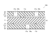
- a laminate 10A is prepared.
- the laminate 10A one in which a buildup precursor layer 20A is laminated on the core substrate 10 is used. If necessary, a buildup precursor layer 50A may be laminated on the core substrate 10 on the side opposite to the buildup precursor layer 20A with respect to the core substrate 10.
- the laminate 10A includes a base layer 54, an insulating layer 51, a core substrate 10, an insulating layer 21, and a base layer 24 as shown in FIG. 6, which are arranged in this order.
- the buildup precursor layer 20A includes an insulating layer 21 and a base layer 24.
- the buildup precursor layer 50A includes an insulating layer 51 and a base layer 54.
- the base layers 24 and 54 have not yet been formed into a wiring pattern. No hole 21a is formed in the insulating layer 21, and no hole 51a is formed in the insulating layer 51. At this point, the thickness of the base layers 24, 54 is, for example, 3 ⁇ m or more and 18 ⁇ m or less. The thickness of the insulating layer 21 is, for example, 40 to 100 ⁇ m.
- Preparation of the laminate 10A is performed, for example, as in (1) or (2) below.
- (1) Prepreg, resin films, etc. are laminated on both sides of the core substrate 10, and metal foil is further laminated on these prepregs, resin films, etc. Thereafter, the prepreg or resin film is cured by heating and pressurizing the metal foil, prepreg, resin film, etc. and the core substrate 10, and is fixed to the core substrate 10 and the metal foil, thereby forming the insulating layers 21, 51 and the lower layer.
- Form strata 24, 54 (2)
- a build-up sheet in which metal foil is laminated in advance on a resin film or the like is laminated on both sides of the core substrate 10. Then, by heating and pressurizing the buildup sheet and core substrate 10, the resin film and the like are cured and fixed to the core substrate 10, thereby forming the insulating layers 21 and 51.
- the surfaces of the base layers 24 and 54 are roughened. Specifically, the surfaces of the base layers 24 and 54 are etched. As a result, the surfaces of the base layers 24, 54 become rough and black, and the base layers 24, 54 become thin.
- the thickness of the base layers 24, 54 after the surface treatment is, for example, 2 ⁇ m or more and 17 ⁇ m or less.
- the laminate 10A is set in a laser beam processing machine, and a mask 110 is set between the laser oscillator of the laser beam processing machine and the base layer 24.
- Mask 110 has at least one circular through hole 111 that passes through mask 110 .
- the diameter of the through hole 111 is, for example, 2 to 3 mm, more specifically 2.4 mm.
- a laser beam processing machine is used to irradiate the base layer 24 with a laser beam 150 through the through hole 111.
- An opening 24a is formed in the base layer 24 at a location irradiated with the laser beam 150. Since the base layer 24 has already been roughened as described above, the laser beam 150 is absorbed by the base layer 24 without being reflected by the base layer 24 .
- the output of the laser beam 150 in the laser beam processing machine is, for example, 10 to 20 mJ/shot, more specifically 16 mJ/shot.
- the diameter of the opening 24a is determined depending on the diameter of the through hole 111 and the output of the laser beam 150. The longer the diameter of the through hole 111, the longer the diameter of the opening 24a, and the higher the output of the laser beam 150, the longer the diameter of the opening 24a. For example, if the diameter of the through hole 111 is 2.4 mm and the output of the laser beam 150 is, for example, 16 mJ/shot, an opening 24a with a diameter of 100 ⁇ m is formed. Note that the output of the laser beam 150 is also referred to as power.
- the irradiation of the laser beam 150 is stopped.
- a plurality of openings 24a are formed in the base layer 24 by changing the irradiation location of the laser beam 150.
- the mask 110 is replaced with a mask 120 and set.
- Mask 120 has at least one circular through hole 121 that passes through mask 120 .
- the diameter of the through hole 121 is shorter than that of the through hole 111 of the mask 110.
- the diameter of the through hole 121 is, for example, 1/3 or more and 1/2 or less of the diameter of the through hole 111, and more specifically, 1.1 mm.
- the insulating layer 21 is irradiated with a laser beam 160 through the through hole 121 and the opening 24a using the laser beam processing machine.
- a cylindrical hole 21a is formed in the insulating layer 21 at the location where the laser beam 160 is irradiated.
- the output of the laser beam 160 is, for example, 1/15 or more and 1/8 or less of the output of the laser beam 150 when the aperture 24a is formed, and more specifically, 1.8 mJ/shot.
- the diameter of the hole 21a formed is shorter than the diameter of the opening 24a.
- the diameter of the hole 21a is determined depending on the diameter of the through hole 121 and the output of the laser beam 160.
- the opening 24a is formed according to the preferred conditions described above, the diameter of the through hole 121 is 1.1 mm, and the output of the laser beam 160 is, for example, 1.8 mJ/shot, then the hole 21a has a diameter of 80 ⁇ m. is formed.
- the irradiation of the laser beam 160 is stopped.
- the laser beam 160 is incident on the surface of the conductor layer 12 for a short time, so that the surface of the conductor layer 12 is shaped into a concave shape by the laser beam 160.
- the laser beam 150 enters around the opening 24a, so a tapered portion 24b is formed around the opening 24a.
- a plurality of holes 21a are formed in the insulating layer 21 by changing the irradiation location of the laser beam 160.
- an opening 54a is formed in the base layer 54 in the same manner as the opening 24a is formed in the base layer 24.
- a hole 51a is formed in the insulating layer 51 in the same manner as the hole 21a is formed in the insulating layer 21.
- the smear in the holes 21a and 51a is removed by, for example, plasma treatment or a permanganic acid aqueous solution. As shown in FIG. 11, such desmear processing enlarges the hole 21a to a diameter equal to that of the opening 24a, and also enlarges the hole 51a to a diameter equal to that of the opening 54a.
- plating Next, plating is performed on the laminate 10A in which the openings 24a, 54a and the holes 21a, 51a are formed, and as shown in FIG. Form layers 25A and 55A.
- wiring patterns are formed on the metal plating layers 25A, 55A and the base layers 24, 54. Specifically, first, a resist is laminated on the metal plating layers 25A and 55A. After exposing the resist to light, the resist is developed. When the metal plated layers 25A, 55A and base layers 24, 54 are etched using the resist as a mask, the metal plated layers 25A, 55A and base layers 24, 54 are shaped into a wiring pattern. The remaining metal plating layer 25A is the upper layer 25 having a wiring pattern, and the remaining metal plating layer 55A is the upper layer 55 having a wiring pattern.
- solder resist layer Next, the first solder resist layer 40 is laminated on the insulating layer 21 and the upper layer 25, and the second solder resist layer 70 is laminated on the insulating layer 51 and the upper layer 55. Through the above steps, printed wiring board 1 is completed.
- the wiring patterns of the base layers 24, 54 and the upper layers 25, 5 are formed by the subtractive method, but may be formed by MSAP (Modified Semi Additive Process).
- the diameter of the through hole 121 through which the laser beam 160 passes is shorter than the diameter of the through hole 111. Therefore, the diameter of the hole 21a formed by the laser beam 160 is smaller than the diameter of the opening 24a formed by the laser beam 150. However, after the hole 21a is formed, the inner wall of the hole 21a may be expanded in diameter by desmear processing, so the diameters of the hole 21a and the opening 24a are likely to be close to or equal to each other.
- the output of the laser beam 160 is preferably set to 1/5 to 1/100 of the output of the laser beam 150. In this way, the base layer 24 can be kept in a state where it does not protrude inward from the edge of the hole 21a.
- the plating solution can be easily circulated within the hole 21a.
- the metal plating grows well within the hole 21a, and the via conductor 22 is well formed. In other words, voids, defects, etc. are less likely to occur in the via conductor 22.
- minute metal crystals are likely to be formed on the inner wall side of the hole 21a, and the via conductors 22 and 52 are more likely to be buried in the unevenness formed on the inner wall of the hole 21a. Further, the metal crystal has few defects from the vicinity of the inner wall of the hole 21a toward the center axis of the via conductors 22 and 52, and tends to have a crystal structure with a well-organized kink structure.
- the opening diameter of the hole 21a distal to the base layer 24 is approximately equal to the opening diameter of the hole 21a proximal to the base layer 24, and the diameter of the hole 21a remains uniform in the thickness direction even after the desmear process.
- the via conductor 22 is formed so that its diameter is uniform over the thickness direction. Therefore, the via conductor 22 is less likely to come out of the insulating layer 21 than when a tapered hole is formed and filled with a conductor, and the contact area between the via conductor 22 and the conductor layer 12 can be increased. The same applies to the via conductor 52.
- the diameter of the through hole 121 through which the laser beam 160 passes is 1/3 or more and 1/2 or less of the diameter of the through hole 111 through which the laser beam 150 passes.
- the output of the laser beam 160 is 1/15 or more and 1/8 or less of the output of the laser beam 150 when the aperture 24a is formed. Therefore, even if the thickness of the insulating layer 21 is 40 to 100 ⁇ m, the difference between the opening diameter of the hole 21a near the base layer 24 and the opening diameter of the hole 21a distal from the base layer 24 is kept to 5 ⁇ m or less. can.
- the opening diameter of the holes 21a distal from the base layer 24 is the same as that of the bottom of a tapered hole. If the diameter of the via conductor 22 is made equal to the opening diameter of the via conductor 22, the diameter of the portion of the via conductor 22 that is proximal to the underlying layer 24 can be reduced. Accordingly, the diameter of the land overlapping the via conductor 22 can also be reduced. When there are multiple via conductors 22, the interval between the via conductors 22 can be shortened. Even if the diameter of the lands is 225 ⁇ m or more and 250 ⁇ m or less and the pitch of the via conductors 22 is 245 ⁇ m, the insulation between the lands and the insulation between the via conductors 22 can be ensured.
- the process for forming the opening 24a in the base layer 24 may be performed using other methods such as a large window method or a conformal mask method.
- the process can be simpler than that using the method.
- the large window method is a method in which an opening is formed in a copper foil by etching, and then a hole with a diameter smaller than the opening is formed in a resin layer by laser beam processing.
- the conformal mask method is a method in which an opening is formed in a copper foil by etching, and then a hole with a diameter larger than the opening is formed in a resin layer by laser beam processing.
- a printed wiring board includes a core substrate, a buildup layer laminated on the core substrate, and the buildup layer includes an insulating layer laminated on the core substrate, and an insulating layer laminated on the core substrate; It has a hole penetrating the insulating layer in the thickness direction and a via conductor filled in the hole, and the via conductor has a cylindrical shape.
- the inner wall surface of the hole has unevenness, and the via conductor is in contact with the inner wall surface.
- the buildup layer has a surface conductor layer on the insulating layer opposite to the core substrate, and the via conductor It has a side surface facing the inner wall surface of the hole, and the side surface has at least one convex portion, and is inclined so that the convex portion faces toward the surface conductor layer.
- the convex portion is inclined toward the core substrate.
- the surface conductor layer has a base layer and an upper layer, the base layer is located on the insulating layer side, and the via It has an opening at a position overlapping the conductor, and the inner edge of the opening is located at a position overlapping with the opening edge of the hole or outside the opening edge of the hole.
- the region on the inner edge side of the opening has a tapered portion, and the thickness of the tapered portion gradually decreases toward the edge of the opening.
- the core substrate has a conductor layer on a surface in contact with the buildup layer, and of the conductor layer, the via conductor The surface of the part where it touches is concave.
- the method for manufacturing a printed wiring board includes the step of preparing a laminate in which a build-up precursor layer comprising an insulating layer and a metal base layer in this order is stacked on a core substrate; A first mask having a first through hole is disposed above the base layer side of the laminate, and a first laser beam is irradiated toward the base layer through the first through hole to remove the base layer.
- the diameter of the second through hole is 1/3 or more and 1/2 or less of the diameter of the first through hole.
- the output of the second laser beam is 1/15 or more and 1/8 or less of the output of the first laser beam.
- the manufacturing method according to any one of (8) to (10) above further includes the step of enlarging the diameter of the hole so as not to exceed the inner edge of the opening of the base layer.
Abstract
Provided are: a printed wiring board having a via conductor which is not easily extracted from an insulating layer; and a method for manufacturing the same. The printed wiring board comprises a core substrate and a buildup layer stacked on the core substrate. The buildup layer has an insulating layer stacked on the core substrate, a hole passing through the insulating layer in the thickness direction of the insulating layer, and a via conductor filled in the hole. The shape of the via conductor is cylindrical.
Description
本開示は、印刷配線板及びその製造方法に関する。
The present disclosure relates to a printed wiring board and a method for manufacturing the same.
従来、コア基板の少なくとも一方の面にビルドアップ層が積層された印刷配線板が開示されている(例えば、特許文献1)。ビルドアップ層にはビア導体が設けられている。このビア導体は、コア基板の表面のメッキ配線とビルドアップ層の表面のメッキ配線とに接続される。これらメッキ配線は、ビア導体によって電気的に導通される。
Conventionally, a printed wiring board in which a build-up layer is laminated on at least one surface of a core substrate has been disclosed (for example, Patent Document 1). Via conductors are provided in the buildup layer. This via conductor is connected to the plated wiring on the surface of the core substrate and the plated wiring on the surface of the buildup layer. These plated wirings are electrically connected by via conductors.
ところで、近年、電子機器の小型化に伴い、印刷配線板を薄くするための技術開発が行われている。ビルドアップ層を薄くするための技術開発も進み、ビア導体を小径にするための技術開発も進んでいる。ビルドアップ層が薄く、ビア導体が小径であると、ビア導体とその周囲の絶縁層の接触面積が小さく、ビア導体とメッキ配線の接触面積が小さい。そのため、ビア導体が絶縁層から抜けやすいという課題がある。
Incidentally, in recent years, with the miniaturization of electronic devices, technological developments have been made to make printed wiring boards thinner. Technological developments are progressing to make the build-up layer thinner, and technological developments are also progressing to make via conductors smaller in diameter. When the buildup layer is thin and the via conductor has a small diameter, the contact area between the via conductor and the surrounding insulating layer is small, and the contact area between the via conductor and the plated wiring is small. Therefore, there is a problem that the via conductor easily comes off from the insulating layer.
本開示の一態様は、
コア基板と、
前記コア基板に積層されるビルドアップ層と、を備え、
前記ビルドアップ層が、
前記コア基板に積層される絶縁層と、
前記絶縁層を厚み方向に貫通するホールと、
該ホールに充填されたビア導体と、
を有し、
前記ビア導体の形状が、円柱状である
印刷配線板である。 One aspect of the present disclosure is
core board,
a build-up layer laminated on the core substrate,
The buildup layer is
an insulating layer laminated on the core substrate;
a hole penetrating the insulating layer in the thickness direction;
a via conductor filled in the hole;
has
The printed wiring board has the via conductor having a cylindrical shape.
本開示の一態様は、
コア基板に、絶縁層及び金属製の下地層をこの順に備えたビルドアップ前駆体層が重ねられた積層体を準備する工程と、
前記積層体の前記下地層側の上方に、第1貫通孔を有する第1のマスクを配置し、第1のレーザービームを前記第1貫通孔を通じて前記下地層に向けて照射して前記下地層に開口を形成する工程と、
前記下地層の前記第1貫通孔の上方に、前記第1貫通孔よりも径の小さい第2貫通孔を有する第2のマスクを配置し、前記開口を通じて第2のレーザービームを前記絶縁層に向けて照射して、前記絶縁層にホールを形成する工程と、
該ホールを形成した前記絶縁層に対してメッキ処理を行い、前記下地層及び前記ホールにメッキ膜を成長させてビア導体および上層を形成する工程と、
を含む印刷配線板の製造方法である。 One aspect of the present disclosure is
preparing a laminate in which a build-up precursor layer comprising an insulating layer and a metal underlayer in this order is stacked on a core substrate;
A first mask having a first through hole is disposed above the base layer side of the laminate, and a first laser beam is irradiated toward the base layer through the first through hole to remove the base layer. forming an opening in the
A second mask having a second through hole smaller in diameter than the first through hole is disposed above the first through hole in the base layer, and a second laser beam is directed to the insulating layer through the opening. forming a hole in the insulating layer by irradiating the
plating the insulating layer in which the hole is formed, and growing a plating film on the base layer and the hole to form a via conductor and an upper layer;
A method of manufacturing a printed wiring board including:
本開示の内容によれば、ビア導体が絶縁層から抜けにくい。
According to the content of the present disclosure, the via conductor is difficult to come out of the insulating layer.
以下、図面を参照して、実施形態について説明する。ただし、以下で参照する各図は、説明の便宜上、実施形態を説明する上で必要な主要部材のみを簡略化して示したものである。したがって、本開示の印刷配線板1は、図面に示されていない任意の構成部材を備え得る。また、図面の部材の寸法は、実際の構成部材の寸法および寸法比率などを忠実に表したものではない。
Hereinafter, embodiments will be described with reference to the drawings. However, for convenience of explanation, each figure referred to below shows only the main members necessary for explaining the embodiment in a simplified manner. Therefore, the printed wiring board 1 of the present disclosure may include any constituent members not shown in the drawings. Further, the dimensions of the members in the drawings do not faithfully represent the dimensions and dimensional ratios of the actual constituent members.
[1. 印刷配線板]
図1を参照して、印刷配線板1について説明する。
印刷配線板1は、多層基板である。印刷配線板1は、コア基板10及び第1のビルドアップ層20を有する。なお、この印刷配線板1は、必要に応じて、図1に示すように、第1のソルダーレジスト層40、第2のビルドアップ層50及び第2のソルダーレジスト層70を備える。第2のソルダーレジスト層70、第2のビルドアップ層50、コア基板10、第1のビルドアップ層20及び第1のソルダーレジスト層40がこれらの順に積層されている構成であってもよい。 [1. Printed wiring board]
A printedwiring board 1 will be explained with reference to FIG.
Printedwiring board 1 is a multilayer board. Printed wiring board 1 has a core substrate 10 and a first buildup layer 20. In addition, this printed wiring board 1 is provided with the 1st solder resist layer 40, the 2nd buildup layer 50, and the 2nd solder resist layer 70 as shown in FIG. 1 as needed. The second solder resist layer 70, the second buildup layer 50, the core substrate 10, the first buildup layer 20, and the first solder resist layer 40 may be stacked in this order.
図1を参照して、印刷配線板1について説明する。
印刷配線板1は、多層基板である。印刷配線板1は、コア基板10及び第1のビルドアップ層20を有する。なお、この印刷配線板1は、必要に応じて、図1に示すように、第1のソルダーレジスト層40、第2のビルドアップ層50及び第2のソルダーレジスト層70を備える。第2のソルダーレジスト層70、第2のビルドアップ層50、コア基板10、第1のビルドアップ層20及び第1のソルダーレジスト層40がこれらの順に積層されている構成であってもよい。 [1. Printed wiring board]
A printed
Printed
[1-1. コア基板]
コア基板10は、基材11及び導体層12,13を有する。
基材11は平板状に成している。基材11は、第1表面11aと、その第1表面11aの反対側の第2表面11bとを有する。第1表面11aと第2表面11bは互いに反対を向いている。基材11は、第1表面11aから第2表面11bまでの厚みを有する。第1表面11aから第2表面11bの方への方向及びその逆方向は、厚み方向である。 [1-1. Core board]
Thecore substrate 10 has a base material 11 and conductor layers 12 and 13.
Thebase material 11 has a flat plate shape. The base material 11 has a first surface 11a and a second surface 11b opposite to the first surface 11a. The first surface 11a and the second surface 11b face oppositely to each other. The base material 11 has a thickness from the first surface 11a to the second surface 11b. The direction from the first surface 11a to the second surface 11b and the opposite direction are the thickness directions.
コア基板10は、基材11及び導体層12,13を有する。
基材11は平板状に成している。基材11は、第1表面11aと、その第1表面11aの反対側の第2表面11bとを有する。第1表面11aと第2表面11bは互いに反対を向いている。基材11は、第1表面11aから第2表面11bまでの厚みを有する。第1表面11aから第2表面11bの方への方向及びその逆方向は、厚み方向である。 [1-1. Core board]
The
The
基材11は、絶縁性を有する素材から形成されている。このような絶縁性の素材としては、例えば、エポキシ樹脂、ビスマレイミド-トリアジン樹脂、ポリイミド樹脂、ポリフェニレンエーテル(PPE)樹脂、ポリフェニレンオキシド(PPO)樹脂、シアネートエステル樹脂及び液晶ポリマーなどのような有機樹脂が挙げられる。これらの有機樹脂のうち2種以上が混合されていてもよい。これら有機樹脂のうちの1種又は2種以上に補強材が配合されてもよい。補強材としては、例えば、ガラス繊維、ガラス不織布、アラミド繊維、アラミド不織布、ポリエステル繊維及びポリエステル不織布のような布材が挙げられる。これらの有機樹脂のうちの1種又は2種以上に、例えば硫酸バリウム、タルク、クレー、ガラス、炭酸カルシウム及びチタンなどのような無機充填材が含まれてもよい。
The base material 11 is made of an insulating material. Examples of such insulating materials include organic resins such as epoxy resins, bismaleimide-triazine resins, polyimide resins, polyphenylene ether (PPE) resins, polyphenylene oxide (PPO) resins, cyanate ester resins, and liquid crystal polymers. can be mentioned. Two or more types of these organic resins may be mixed. A reinforcing material may be blended with one or more of these organic resins. Examples of the reinforcing material include cloth materials such as glass fiber, glass nonwoven fabric, aramid fiber, aramid nonwoven fabric, polyester fiber, and polyester nonwoven fabric. One or more of these organic resins may contain inorganic fillers such as barium sulfate, talc, clay, glass, calcium carbonate, titanium, and the like.
導体層12は、基材11の第1表面11aに積層されている。導体層13は、基材11の第2表面11bに積層されている。導体層12,13は、配線パターンに成している。導体層12,13の材質は、例えば銅のような導電性金属である。導体層12,13は、例えば銅メッキのような金属メッキからなる。導体層12,13の厚さは、例えば18μm以上100μm以下であるのがよい。
The conductor layer 12 is laminated on the first surface 11a of the base material 11. The conductor layer 13 is laminated on the second surface 11b of the base material 11. The conductor layers 12 and 13 are formed into a wiring pattern. The material of the conductor layers 12 and 13 is, for example, a conductive metal such as copper. The conductor layers 12 and 13 are made of metal plating such as copper plating, for example. The thickness of the conductor layers 12 and 13 is preferably 18 μm or more and 100 μm or less, for example.
なお、コア基板10は多層構造であってもよい。その多層構造としては、以下に示す態様を一例として挙げることができる。例えば、多層構造は、複数の絶縁層、1つ又は複数の内部導体層及び2つの表面導体層を有する。絶縁層は順に積層されている。内部導体層はこれら絶縁層の間に挟まれている。2つの表面導体層は、導体層12,13が基材11の表面11a,11bにそれぞれ積層されるのと同様にして、複数の絶縁層からなる積層体の2つの最表面にそれぞれ積層されている。内部導体層及び表面導体層は、配線パターンを成している。
Note that the core substrate 10 may have a multilayer structure. Examples of the multilayer structure include the following embodiments. For example, a multilayer structure has multiple insulating layers, one or more inner conductor layers and two surface conductor layers. The insulating layers are laminated in order. An inner conductor layer is sandwiched between these insulating layers. The two surface conductor layers are laminated on the two outermost surfaces of a laminate made of a plurality of insulating layers, in the same way that the conductor layers 12 and 13 are laminated on the surfaces 11a and 11b of the base material 11, respectively. There is. The inner conductor layer and the surface conductor layer form a wiring pattern.
[1-2. ビルドアップ層]
第1のビルドアップ層20は、絶縁層21、少なくとも1つのビア導体22及び表面導体層23を有する。 [1-2. Buildup layer]
Thefirst buildup layer 20 has an insulating layer 21 , at least one via conductor 22 and a surface conductor layer 23 .
第1のビルドアップ層20は、絶縁層21、少なくとも1つのビア導体22及び表面導体層23を有する。 [1-2. Buildup layer]
The
絶縁層21は、コア基板10の表面に積層されている。つまり、絶縁層21は、導体層12を被覆するとともに、基材11の第1表面11aも被覆している。言い換えれば、コア基板10は、ビルドアップ層20に接する面に導体層12を有している。絶縁層21の厚さは、つまり、導体層12に関して第1表面11aに接する表面12cと反対側の導体層12の表面12dから、絶縁層21に関してコア基板10と反対側の絶縁層21の表面21dまでの厚さは、例えば40~100μmである。
The insulating layer 21 is laminated on the surface of the core substrate 10. That is, the insulating layer 21 covers the conductor layer 12 and also covers the first surface 11a of the base material 11. In other words, the core substrate 10 has the conductor layer 12 on the surface in contact with the buildup layer 20. The thickness of the insulating layer 21 is, in other words, from the surface 12d of the conductor layer 12 on the opposite side to the surface 12c in contact with the first surface 11a with respect to the conductor layer 12, to the surface of the insulating layer 21 on the opposite side to the core substrate 10 with respect to the insulating layer 21. The thickness up to 21d is, for example, 40 to 100 μm.
絶縁層21は、絶縁性を有する素材から形成されている。このような絶縁性の素材としては、例えば、エポキシ樹脂、ビスマレイミド-トリアジン樹脂、ポリイミド樹脂、ポリフェニレンエーテル(PPE)樹脂、ポリフェニレンオキシド(PPO)樹脂、シアネートエステル樹脂、ポリテトラフルオロエチレン(PTFE)樹脂及び液晶ポリマーなどのような有機樹脂が挙げられる。これらの有機樹脂のうち2種以上が混合されていてもよい。これら有機樹脂のうちの1種又は2種以上に補強材が配合されてもよい。補強材としては、例えば、ガラス繊維、ガラス不織布、アラミド繊維、アラミド不織布、ポリエステル繊維及びポリエステル不織布のような布材が挙げられる。これらの有機樹脂のうちの1種又は2種以上に、例えば硫酸バリウム、タルク、クレー、ガラス、炭酸カルシウム及びチタンなどのような無機充填材が含まれてもよい。
The insulating layer 21 is made of an insulating material. Examples of such insulating materials include epoxy resin, bismaleimide-triazine resin, polyimide resin, polyphenylene ether (PPE) resin, polyphenylene oxide (PPO) resin, cyanate ester resin, and polytetrafluoroethylene (PTFE) resin. and organic resins such as liquid crystal polymers. Two or more types of these organic resins may be mixed. A reinforcing material may be blended with one or more of these organic resins. Examples of the reinforcing material include cloth materials such as glass fiber, glass nonwoven fabric, aramid fiber, aramid nonwoven fabric, polyester fiber, and polyester nonwoven fabric. One or more of these organic resins may contain inorganic fillers such as barium sulfate, talc, clay, glass, calcium carbonate, titanium, and the like.
ビア導体22は、絶縁層21を厚み方向に貫通している。具体的には、絶縁層21は、厚み方向に絶縁層21を貫通する少なくとも1つのホール21aを有し、ビア導体22がホール21aにそれぞれ充填される構成となっている。ビア導体22の材質は、例えば銅のような導電性金属である。ビア導体22は、コア基板10の導体層12に結合するとともに、その導体層12に電気的に接続されている。
The via conductor 22 penetrates the insulating layer 21 in the thickness direction. Specifically, the insulating layer 21 has at least one hole 21a penetrating the insulating layer 21 in the thickness direction, and the via conductor 22 is filled in each hole 21a. The material of the via conductor 22 is, for example, a conductive metal such as copper. The via conductor 22 is coupled to the conductor layer 12 of the core substrate 10 and is electrically connected to the conductor layer 12 .
なお、複数のビア導体22が配置される場合、これらビア導体22のピッチは245μmであっても十分な絶縁性を確保できる。
なお、ビルドアップ層20は、絶縁層21と上層25との間に下地層24を有していても良い。下地層24は導電性を有する方がよい。下地層24は金属膜であるのがよい。 Note that when a plurality of viaconductors 22 are arranged, sufficient insulation can be ensured even if the pitch of these via conductors 22 is 245 μm.
Note that thebuildup layer 20 may have a base layer 24 between the insulating layer 21 and the upper layer 25. The base layer 24 is preferably electrically conductive. The base layer 24 is preferably a metal film.
なお、ビルドアップ層20は、絶縁層21と上層25との間に下地層24を有していても良い。下地層24は導電性を有する方がよい。下地層24は金属膜であるのがよい。 Note that when a plurality of via
Note that the
図2は、図1中の領域IIの拡大図である。図2に示すように、導体層12のうちビア導体22が接する部分の表面12aは、凹面状となっていてもよい。つまり、導体層12のうち、ビア導体22が接している部分が凹状になっていると、その凹みにビア導体22の底22aが入り込む状態となる。導体層12とビア導体22との接触面積が大きくなる。これにより導体層12とビア導体22との間の接合力を高めることが可能になる。この場合、ビア導体22の導体層12側の端面は凸面状となっているのがよい。こうしてビア導体22の底22aは、凹面状の表面12aに嵌められる。
FIG. 2 is an enlarged view of region II in FIG. 1. As shown in FIG. 2, the surface 12a of the portion of the conductor layer 12 that is in contact with the via conductor 22 may have a concave shape. In other words, if the portion of the conductor layer 12 that is in contact with the via conductor 22 is recessed, the bottom 22a of the via conductor 22 will fit into the recess. The contact area between conductor layer 12 and via conductor 22 becomes larger. This makes it possible to increase the bonding force between the conductor layer 12 and the via conductor 22. In this case, it is preferable that the end surface of the via conductor 22 on the conductor layer 12 side has a convex shape. In this way, the bottom 22a of the via conductor 22 is fitted into the concave surface 12a.
図1に示すように、巨視的には、ビア導体22が、絶縁層21の厚み方向に沿った中心軸の周りの円柱状に形作られている。ここで、円柱状とは、ビア導体22の直径が厚み方向に亘って一様であるものをいう。ビア導体22は厚み方向の全体に亘ってホール21aの内壁面に接している。図2に示すように、微視的には、ホール21aの内壁面が凹凸のある形状であり、ビア導体22が厚み方向全体に亘ってホール21a内壁面の凹凸にまで充填されている。つまり、ビア導体22が凹凸に形成され、ビア導体22の凹凸がホール21aの内壁面の凹凸に隙間無く噛み合っている。
As shown in FIG. 1, macroscopically, the via conductor 22 is shaped like a cylinder around a central axis along the thickness direction of the insulating layer 21. Here, the term cylindrical means that the diameter of the via conductor 22 is uniform over the thickness direction. The via conductor 22 is in contact with the inner wall surface of the hole 21a throughout its thickness. As shown in FIG. 2, microscopically, the inner wall surface of the hole 21a has an uneven shape, and the via conductor 22 is filled up to the unevenness of the inner wall surface of the hole 21a throughout the thickness direction. In other words, the via conductor 22 is formed in an uneven manner, and the unevenness of the via conductor 22 meshes with the unevenness of the inner wall surface of the hole 21a without any gaps.
図3及び図4は、ビア導体22とホール21aの内壁面の境界の断面の拡大図である。図4に示される部分は、図3に示される部分と異なる位置である。図3及び図4に示すように、ビア導体22の凹凸は、少なくとも1つの凸部22b及び少なくとも1つの凸部22cを有する。凸部22b,22cは、径方向外方に向けて突出するとともに、絶縁層21に刺さっている。言い換えると、凸部22b,22cは、径方向外方に向けて突出している。また、凸部22b,22cは、絶縁層21に刺さるような配置となっている。この場合、凸部22bは、表面導体層23の方へ傾斜する向きとなっている。あるいは、凸部22bは、上層25の方へ傾斜する向きとなっている。さらに言い換えると、凸部22bは、ビア導体22の側面から斜めの向きとなっており、その向きは表面導体層23または上層25の方へ向いている。凸部22cは、コア基板10の方へ傾斜する向きとなっている。言い換えると、凸部22cは、ビア導体22の側面から斜めの向きとなっており、その向きはコア基板10の方へ向いている。
3 and 4 are enlarged cross-sectional views of the boundary between the via conductor 22 and the inner wall surface of the hole 21a. The portion shown in FIG. 4 is in a different position than the portion shown in FIG. As shown in FIGS. 3 and 4, the unevenness of the via conductor 22 has at least one convex portion 22b and at least one convex portion 22c. The protrusions 22b and 22c protrude radially outward and pierce the insulating layer 21. In other words, the convex portions 22b and 22c protrude radially outward. Further, the convex portions 22b and 22c are arranged so as to pierce the insulating layer 21. In this case, the convex portion 22b is oriented toward the surface conductor layer 23. Alternatively, the convex portion 22b is oriented toward the upper layer 25. In other words, the convex portion 22b is oriented diagonally from the side surface of the via conductor 22, and is oriented toward the surface conductor layer 23 or the upper layer 25. The convex portion 22c is oriented toward the core substrate 10. In other words, the convex portion 22c is oriented diagonally from the side surface of the via conductor 22, and is oriented toward the core substrate 10.
図1に示すように、表面導体層23は、絶縁層21に関してコア基板10と反対側の、絶縁層21の表面21dに積層されている。表面導体層23は、配線パターンを成している。表面導体層23は、ビア導体22に電気的に接続されている。
As shown in FIG. 1, the surface conductor layer 23 is laminated on the surface 21d of the insulating layer 21 on the side opposite to the core substrate 10 with respect to the insulating layer 21. The surface conductor layer 23 forms a wiring pattern. The surface conductor layer 23 is electrically connected to the via conductor 22.
表面導体層23は、下地層24及び上層25を有していてもよい。ここで、上層25とは、表面導体層23のうち、下地層24を介して絶縁層21の反対側に位置する金属膜のことである。上層25は表面導体層23を構成している金属膜の一部である。下地層24及び上層25は、これらの順に、絶縁層21に関してコア基板10と反対側の、絶縁層21の表面21dに積層される配置となっている。下地層24の厚さは、例えば2μm以上17μm以下である。下地層24及び上層25は、配線パターンを成している。下地層24及び上層25の材質は、例えば銅のような導電性金属である。
The surface conductor layer 23 may have a base layer 24 and an upper layer 25. Here, the upper layer 25 is a metal film located on the opposite side of the insulating layer 21 with the base layer 24 in the surface conductor layer 23 . The upper layer 25 is a part of the metal film that constitutes the surface conductor layer 23. The base layer 24 and the upper layer 25 are arranged to be laminated in this order on the surface 21d of the insulating layer 21 on the opposite side of the core substrate 10 with respect to the insulating layer 21. The thickness of the base layer 24 is, for example, 2 μm or more and 17 μm or less. The base layer 24 and the upper layer 25 form a wiring pattern. The material of the base layer 24 and the upper layer 25 is, for example, a conductive metal such as copper.
下地層24は、ホール21aに重なる位置に開口24aを有する。開口24aの内縁は、ホール21aの開口縁と重なる位置、またはホール21aの開口縁よりも外側に位置している。下地層24は、開口24aの周囲にテーパー部24bを有する。ここで、開口24aの周囲とは、開口24aの内縁(または縁)を含み、その内縁から法線方向に所定の幅で広がる領域のことである。テーパー部24bの厚さは、開口24aの縁に向かうほど漸減する。言い換えると、下地層24は、開口24aの縁から外側への法線の方向に向かうにしたがって厚みが厚くなっているのがよい。下地層24が開口24aの縁から外側への法線の方向に向かうにしたがって厚みが厚くなる形状であると、この下地層24のテーパー部24bが絶縁層21から剥離しにくくなる確率が高くなる。下地層24のテーパー部24bの付近は、絶縁層21、ビア導体22および上層25といった複数の部材が互いに接している部位である。複数の部材が互いに接している部位には、各部材の熱膨張率、ヤング率の違いから応力が発生しやすい。このような場合に、下地層24が開口24aの縁から外側への法線の方向に向かうにしたがって厚みが厚くなる形状であると、テーパー部24bの端である開口24aの縁付近に発生しやすい応力を低減することができる。この場合、特に、下地層24の厚みが開口24aの縁の方に向けて厚みが薄くなっているのがよい。さらには、テーパー部24bの上層25に接する表面が上層25側に凸の湾曲した形状を成しているのがよい。上層25は、開口24aを通じてビア導体22に連なり、ビア導体22は上層25と一体である。上層25のうち、テーパー部24bの重なる部分の厚さは、開口24aの縁に向かうほど漸減する。開口24aの縁におけるテーパー部24bの角度θは、例えば45°を超え、より具体的には50°以上80°以下であるのがよい。
The base layer 24 has an opening 24a at a position overlapping the hole 21a. The inner edge of the opening 24a is located at a position that overlaps with the opening edge of the hole 21a or outside the opening edge of the hole 21a. The base layer 24 has a tapered portion 24b around the opening 24a. Here, the periphery of the opening 24a refers to an area that includes the inner edge (or edge) of the opening 24a and extends from the inner edge by a predetermined width in the normal direction. The thickness of the tapered portion 24b gradually decreases toward the edge of the opening 24a. In other words, it is preferable that the thickness of the base layer 24 increases in the direction of the normal line outward from the edge of the opening 24a. If the base layer 24 has a shape in which the thickness increases as it goes in the direction of the normal line outward from the edge of the opening 24a, the probability that the tapered portion 24b of the base layer 24 will be difficult to peel off from the insulating layer 21 increases. . The vicinity of the tapered portion 24b of the base layer 24 is a region where a plurality of members such as the insulating layer 21, the via conductor 22, and the upper layer 25 are in contact with each other. Stress is likely to occur in areas where multiple members are in contact with each other due to differences in coefficient of thermal expansion and Young's modulus of each member. In such a case, if the base layer 24 has a shape in which the thickness increases from the edge of the opening 24a toward the outside in the direction of the normal line, cracks may occur near the edge of the opening 24a, which is the end of the tapered portion 24b. Easy stress can be reduced. In this case, it is particularly preferable that the thickness of the base layer 24 becomes thinner toward the edge of the opening 24a. Furthermore, it is preferable that the surface of the tapered portion 24b in contact with the upper layer 25 has a curved shape convex toward the upper layer 25 side. The upper layer 25 is connected to the via conductor 22 through the opening 24a, and the via conductor 22 is integral with the upper layer 25. The thickness of the portion of the upper layer 25 where the tapered portion 24b overlaps gradually decreases toward the edge of the opening 24a. The angle θ of the tapered portion 24b at the edge of the opening 24a is, for example, more than 45°, and more specifically preferably 50° or more and 80° or less.
なお、表面導体層23のうちビア導体22と重なる部分は、配線パターンの線幅よりも長い直径を有したランドである。ランドの直径としては、例えば200μm以上250μm以下であるのがよい。
Note that the portion of the surface conductor layer 23 that overlaps with the via conductor 22 is a land having a diameter longer than the line width of the wiring pattern. The diameter of the land is preferably 200 μm or more and 250 μm or less, for example.
上述したように、印刷配線板1は、第2のビルドアップ層50を有していても良い。第2のビルドアップ層50は、コア基板10の第1のビルドアップ層20が位置する表面とは反対側の表面に位置する。コア基板10は、第2のビルドアップ層50に接する面に導体層13を有していてもよい。第2のビルドアップ層50は、絶縁層51、少なくとも1つのビア導体52及び表面導体層53を有する。第2のビルドアップ層50は、第1のビルドアップ層20と同様に設けられている。第2のビルドアップ層50の絶縁層51は第1のビルドアップ層20の絶縁層21に相当し、第2のビルドアップ層50のビア導体52は第1のビルドアップ層20のビア導体22に相当し、第2のビルドアップ層50の表面導体層53は第1のビルドアップ層20の表面導体層23に相当する。また、絶縁層51のホール51aは絶縁層21のホール21aに相当し、表面導体層53の下地層54は表面導体層23の下地層24に相当し、表面導体層53の上層55は表面導体層23の上層25に相当し、下地層54の開口54aは下地層24の開口24aに相当する。また、下地層24が開口24aの周囲にテーパー部を有するのと同様に、下地層54は、開口54aの縁に向かうほど厚さが漸減するテーパー部を開口の周囲に有する。
As mentioned above, the printed wiring board 1 may have the second buildup layer 50. The second buildup layer 50 is located on the surface of the core substrate 10 opposite to the surface on which the first buildup layer 20 is located. Core substrate 10 may have conductor layer 13 on the surface in contact with second buildup layer 50 . The second buildup layer 50 has an insulating layer 51, at least one via conductor 52, and a surface conductor layer 53. The second buildup layer 50 is provided similarly to the first buildup layer 20. The insulating layer 51 of the second buildup layer 50 corresponds to the insulating layer 21 of the first buildup layer 20, and the via conductor 52 of the second buildup layer 50 corresponds to the via conductor 22 of the first buildup layer 20. The surface conductor layer 53 of the second buildup layer 50 corresponds to the surface conductor layer 23 of the first buildup layer 20. Further, the hole 51a of the insulating layer 51 corresponds to the hole 21a of the insulating layer 21, the base layer 54 of the surface conductor layer 53 corresponds to the base layer 24 of the surface conductor layer 23, and the upper layer 55 of the surface conductor layer 53 corresponds to the base layer 24 of the surface conductor layer 23. This corresponds to the upper layer 25 of the layer 23 , and the opening 54 a of the base layer 54 corresponds to the opening 24 a of the base layer 24 . Further, in the same way that the base layer 24 has a tapered part around the opening 24a, the base layer 54 has a tapered part around the opening whose thickness gradually decreases toward the edge of the opening 54a.
[1-3. ソルダーレジスト層]
ソルダーレジスト層40,70は、第1のビルドアップ層20、コア基板10及び第2のビルドアップ層50の積層体の両面にそれぞれ積層されている。つまり、第1のソルダーレジスト層40は、表面導体層23を被覆するとともに、絶縁層21に関してコア基板10と反対側の絶縁層21の表面21dを被覆している。第2のソルダーレジスト層70は、表面導体層53を被覆するとともに、絶縁層51に関してコア基板10と反対側の絶縁層51の表面51dを被覆している。 [1-3. Solder resist layer]
The solder resist layers 40 and 70 are laminated on both sides of the laminate of the first buildup layer 20, core substrate 10, and second buildup layer 50, respectively. That is, the first solder resist layer 40 covers the surface conductor layer 23 and also covers the surface 21 d of the insulating layer 21 on the side opposite to the core substrate 10 with respect to the insulating layer 21 . The second solder resist layer 70 covers the surface conductor layer 53 and also covers the surface 51 d of the insulating layer 51 on the side opposite to the core substrate 10 with respect to the insulating layer 51 .
ソルダーレジスト層40,70は、第1のビルドアップ層20、コア基板10及び第2のビルドアップ層50の積層体の両面にそれぞれ積層されている。つまり、第1のソルダーレジスト層40は、表面導体層23を被覆するとともに、絶縁層21に関してコア基板10と反対側の絶縁層21の表面21dを被覆している。第2のソルダーレジスト層70は、表面導体層53を被覆するとともに、絶縁層51に関してコア基板10と反対側の絶縁層51の表面51dを被覆している。 [1-3. Solder resist layer]
The solder resist
第1のソルダーレジスト層40は、少なくとも1つの開口41を有する。表面導体層23の一部が開口41に重なり、表面導体層23のうち開口41内の部分が端子である。第2のソルダーレジスト層70も第1のソルダーレジスト層40と同様に、少なくとも1つの開口71を有する。表面導体層53の一部が開口71に重なり、表面導体層53のうち開口71内の部分が端子である。
The first solder resist layer 40 has at least one opening 41. A portion of the surface conductor layer 23 overlaps the opening 41, and the portion of the surface conductor layer 23 inside the opening 41 is a terminal. Like the first solder resist layer 40, the second solder resist layer 70 also has at least one opening 71. A portion of the surface conductor layer 53 overlaps the opening 71, and the portion of the surface conductor layer 53 inside the opening 71 is a terminal.
[1-4. 変形例]
(1) 図1に示す例では、第1のビルドアップ層20の数が1である。それに対して、複数の第1のビルドアップ層20がコア基板10と第1のソルダーレジスト層40の間において積層されてもよい。同様に、複数の第2のビルドアップ層50がコア基板10と第2のソルダーレジスト層70の間において積層されてもよい。
第1のビルドアップ層20が、コア基板10の直上から数えてn層ある場合、2からn層目の第1のビルドアップ層20のビア導体22は、直下の第1のビルドアップ層20の表面導体層23に電気的に接続されている。第2のビルドアップ層50がn層あるビア導体52についても同様である。 [1-4. Modified example]
(1) In the example shown in FIG. 1, the number of first buildup layers 20 is one. On the other hand, a plurality of first buildup layers 20 may be stacked between thecore substrate 10 and the first solder resist layer 40. Similarly, a plurality of second buildup layers 50 may be stacked between the core substrate 10 and the second solder resist layer 70.
When there are n first buildup layers 20 counting from directly above thecore substrate 10, the via conductors 22 of the second to nth first buildup layers 20 are connected to the first buildup layers 20 directly below the core substrate 10. It is electrically connected to the surface conductor layer 23 of. The same applies to the via conductor 52 having n second buildup layers 50.
(1) 図1に示す例では、第1のビルドアップ層20の数が1である。それに対して、複数の第1のビルドアップ層20がコア基板10と第1のソルダーレジスト層40の間において積層されてもよい。同様に、複数の第2のビルドアップ層50がコア基板10と第2のソルダーレジスト層70の間において積層されてもよい。
第1のビルドアップ層20が、コア基板10の直上から数えてn層ある場合、2からn層目の第1のビルドアップ層20のビア導体22は、直下の第1のビルドアップ層20の表面導体層23に電気的に接続されている。第2のビルドアップ層50がn層あるビア導体52についても同様である。 [1-4. Modified example]
(1) In the example shown in FIG. 1, the number of first buildup layers 20 is one. On the other hand, a plurality of first buildup layers 20 may be stacked between the
When there are n first buildup layers 20 counting from directly above the
(2) 図2に示す例では、ビア導体22及びホール21aの直径が厚み方向に亘って一様である。それに対して、図5に示すように、ホール21aのうち導体層12に近位の部分21eの直径が開口24a側から導体層12に向かうほど漸減し、その部分21eがテーパー化されていてもよい。それに合わせて、ビア導体22のうち導体層12に近位の部分の直径が開口24a側から導体層12に向かうほど漸減し、その部分21eがテーパー化されている。
(2) In the example shown in FIG. 2, the diameters of the via conductor 22 and the hole 21a are uniform over the thickness direction. On the other hand, as shown in FIG. 5, the diameter of the portion 21e of the hole 21a that is proximal to the conductor layer 12 gradually decreases from the opening 24a side toward the conductor layer 12, and even if the portion 21e is tapered. good. Accordingly, the diameter of the portion of the via conductor 22 near the conductor layer 12 gradually decreases from the opening 24a side toward the conductor layer 12, and the portion 21e is tapered.
[1-5. まとめ]
(1) 従来のように、ビア導体の直径がソルダーレジスト層側からコア基板側に向かうほど漸減し、ビア導体が円錐台型に成していれば、ビア導体が絶縁層から抜けやすい。それに対して、上述のビア導体22,52の直径が厚み方向に亘って一様であり、ビア導体22,52が円柱型に成している。そのため、従来のビア導体と比較して、ビア導体22,52が絶縁層21,51から抜けにくい。 [1-5. summary]
(1) If the diameter of the via conductor gradually decreases from the solder resist layer side toward the core substrate side and the via conductor has a truncated conical shape, as in the past, the via conductor will easily come out of the insulating layer. On the other hand, the diameters of the via conductors 22 and 52 described above are uniform over the thickness direction, and the via conductors 22 and 52 have a cylindrical shape. Therefore, compared to conventional via conductors, the via conductors 22, 52 are less likely to come out from the insulating layers 21, 51.
(1) 従来のように、ビア導体の直径がソルダーレジスト層側からコア基板側に向かうほど漸減し、ビア導体が円錐台型に成していれば、ビア導体が絶縁層から抜けやすい。それに対して、上述のビア導体22,52の直径が厚み方向に亘って一様であり、ビア導体22,52が円柱型に成している。そのため、従来のビア導体と比較して、ビア導体22,52が絶縁層21,51から抜けにくい。 [1-5. summary]
(1) If the diameter of the via conductor gradually decreases from the solder resist layer side toward the core substrate side and the via conductor has a truncated conical shape, as in the past, the via conductor will easily come out of the insulating layer. On the other hand, the diameters of the via
(2) ビア導体22の直径が厚み方向に亘って一様であることは、ビア導体22と導体層12間の接続信頼性の向上に寄与する。ビア導体22と導体層12の結合面積は、従来のビア導体と導体層の結合面積よりも大きい。そのため、従来のビア導体が導体層から離間しやすいのに対して、ビア導体22が導体層12から離間しにくい。同様に、ビア導体52の直径が厚み方向に亘って一様であるため、ビア導体52が導体層13から離間しにくい。
(2) Having a uniform diameter of the via conductor 22 in the thickness direction contributes to improving the connection reliability between the via conductor 22 and the conductor layer 12. The bonding area between the via conductor 22 and the conductor layer 12 is larger than the bonding area between the conventional via conductor and the conductor layer. Therefore, whereas conventional via conductors tend to separate from the conductor layer, the via conductors 22 are difficult to separate from the conductor layer 12. Similarly, since the diameter of the via conductor 52 is uniform over the thickness direction, the via conductor 52 is difficult to separate from the conductor layer 13.
(3) ビア導体22と絶縁層21の熱膨張率が異なることは、導体層12からビア導体22の離間の要因となる。そうであっても、ビア導体52の直径が厚み方向に亘って一様であるため、ビア導体22が導体層12から離間しにくい。
(3) The difference in thermal expansion coefficient between the via conductor 22 and the insulating layer 21 is a factor causing the separation of the via conductor 22 from the conductor layer 12. Even so, since the diameter of the via conductor 52 is uniform over the thickness direction, the via conductor 22 is difficult to separate from the conductor layer 12.
(4) ビア導体22の底22aが凸面状であり、導体層12の表面12aが凹面状であり、ビア導体22の底22aが凹面状の表面12aに嵌められている。このことは、ビア導体22と導体層12間の電気特性の向上に寄与する。具体的には、ビア導体22と導体層12の結合面積が増加するため、ビア導体22と導体層12の境界付近における電気抵抗及び導電率等が安定する。ビア導体52と導体層13についても同様である。
(4) The bottom 22a of the via conductor 22 is convex, the surface 12a of the conductor layer 12 is concave, and the bottom 22a of the via conductor 22 is fitted into the concave surface 12a. This contributes to improving the electrical characteristics between the via conductor 22 and the conductor layer 12. Specifically, since the bonding area between the via conductor 22 and the conductor layer 12 increases, the electrical resistance, conductivity, etc. near the boundary between the via conductor 22 and the conductor layer 12 are stabilized. The same applies to via conductor 52 and conductor layer 13.
(5) ビア導体22の外周とホール21aの内壁面との境界面が凹凸に形成されているため、ビア導体22と絶縁層21の密着性及び接着性が高い上、ビア導体22が絶縁層21から抜けにくい。ビア導体52と絶縁層51についても同様である。
(5) Since the boundary surface between the outer periphery of the via conductor 22 and the inner wall surface of the hole 21a is formed in an uneven manner, the adhesion and adhesion between the via conductor 22 and the insulating layer 21 are high, and the via conductor 22 is formed as an insulating layer. It's hard to get out of 21. The same applies to the via conductor 52 and the insulating layer 51.
(6) ビア導体22の外周の凹凸が少なくとも1つの凸部22bを有し、凸部22bが上層25の方へ傾斜し、凸部22bがホール21aから絶縁層21に刺さっている。凸部22bはビア導体22を絶縁層21にアンカーする。そのため、ビア導体22がホール21aから上層25の方へ抜けにくい上、ビア導体22が導体層12から離間しにくい。ビア導体52についても同様である。
(6) The irregularities on the outer periphery of the via conductor 22 have at least one convex portion 22b, the convex portion 22b is inclined toward the upper layer 25, and the convex portion 22b is inserted into the insulating layer 21 from the hole 21a. The protrusion 22b anchors the via conductor 22 to the insulating layer 21. Therefore, the via conductor 22 is difficult to escape from the hole 21a toward the upper layer 25, and the via conductor 22 is also difficult to separate from the conductor layer 12. The same applies to the via conductor 52.
(7) ビア導体22の外周の凹凸が少なくとも1つの凸部22cを有し、凸部22cがコア基板10の方へ傾斜し、凸部22cがホール21aから絶縁層21に刺さっている。凸部22cはビア導体22を絶縁層21にアンカーする。そのため、上層25の方へ傾斜した凸部22bのみよりもアンカーとしての効果が高まり、ビア導体22が上層25から離間しにくい。ビア導体52についても同様である。
(7) The irregularities on the outer periphery of the via conductor 22 have at least one convex portion 22c, the convex portion 22c is inclined toward the core substrate 10, and the convex portion 22c is inserted into the insulating layer 21 from the hole 21a. The protrusion 22c anchors the via conductor 22 to the insulating layer 21. Therefore, the effect as an anchor is higher than that of only the convex portion 22b inclined toward the upper layer 25, and the via conductor 22 is less likely to be separated from the upper layer 25. The same applies to the via conductor 52.
(8) 下地層24が開口24aの周囲にテーパー部24bを有するため、開口24a付近における下地層24と上層25の接触面積はテーパー部24bがない場合よりも大きくなる。開口24aの周囲における下地層24から上層25の剥離を抑えられ、ひいてはビア導体22が絶縁層21から抜けにくくなる。ビア導体52についても同様である。
(8) Since the base layer 24 has the tapered portion 24b around the opening 24a, the contact area between the base layer 24 and the upper layer 25 near the opening 24a is larger than when there is no tapered portion 24b. Peeling of the upper layer 25 from the base layer 24 around the opening 24a can be suppressed, and as a result, the via conductor 22 becomes difficult to come off from the insulating layer 21. The same applies to the via conductor 52.
[2. 印刷配線板の製造方法]
図6~図13を参照して、印刷配線板1の製造方法について説明する。 [2. Manufacturing method of printed wiring board]
A method for manufacturing printedwiring board 1 will be described with reference to FIGS. 6 to 13.
図6~図13を参照して、印刷配線板1の製造方法について説明する。 [2. Manufacturing method of printed wiring board]
A method for manufacturing printed
[2-1. 準備]
まず、積層体10Aを準備する。積層体10Aとしては、コア基板10にビルドアップ前駆体層20Aが積層されたものを用いる。必要に応じて、コア基板10に関してビルドアップ前駆体層20Aと反対側において、ビルドアップ前駆体層50Aがコア基板10に積層されてもよい。なお、積層体10Aとしては、図6に下地層54、絶縁層51、コア基板10、絶縁層21及び下地層24を有し、これらの順に配置されている。ビルドアップ前駆体層20Aは絶縁層21及び下地層24を有する。ビルドアップ前駆体層50Aは絶縁層51及び下地層54を有する。下地層24,54は、未だ配線パターンに成していない。絶縁層21にはホール21aが形成されておらず、絶縁層51にはホール51aが形成されていない。この時点で下地層24,54の厚さは、例えば3μm以上18μm以下である。絶縁層21の厚さは、例えば40~100μmである。 [2-1. Preparation]
First, alaminate 10A is prepared. As the laminate 10A, one in which a buildup precursor layer 20A is laminated on the core substrate 10 is used. If necessary, a buildup precursor layer 50A may be laminated on the core substrate 10 on the side opposite to the buildup precursor layer 20A with respect to the core substrate 10. Note that the laminate 10A includes a base layer 54, an insulating layer 51, a core substrate 10, an insulating layer 21, and a base layer 24 as shown in FIG. 6, which are arranged in this order. The buildup precursor layer 20A includes an insulating layer 21 and a base layer 24. The buildup precursor layer 50A includes an insulating layer 51 and a base layer 54. The base layers 24 and 54 have not yet been formed into a wiring pattern. No hole 21a is formed in the insulating layer 21, and no hole 51a is formed in the insulating layer 51. At this point, the thickness of the base layers 24, 54 is, for example, 3 μm or more and 18 μm or less. The thickness of the insulating layer 21 is, for example, 40 to 100 μm.
まず、積層体10Aを準備する。積層体10Aとしては、コア基板10にビルドアップ前駆体層20Aが積層されたものを用いる。必要に応じて、コア基板10に関してビルドアップ前駆体層20Aと反対側において、ビルドアップ前駆体層50Aがコア基板10に積層されてもよい。なお、積層体10Aとしては、図6に下地層54、絶縁層51、コア基板10、絶縁層21及び下地層24を有し、これらの順に配置されている。ビルドアップ前駆体層20Aは絶縁層21及び下地層24を有する。ビルドアップ前駆体層50Aは絶縁層51及び下地層54を有する。下地層24,54は、未だ配線パターンに成していない。絶縁層21にはホール21aが形成されておらず、絶縁層51にはホール51aが形成されていない。この時点で下地層24,54の厚さは、例えば3μm以上18μm以下である。絶縁層21の厚さは、例えば40~100μmである。 [2-1. Preparation]
First, a
積層体10Aの準備は、例えば以下の(1)又は(2)のように行われる。
(1) プリプレグまたは樹脂フィルム等をコア基板10の両面に積層し、更にこれらプリプレグまたは樹脂フィルム等に金属箔を積層する。その後、金属箔、プリプレグまたは樹脂フィルム等及びコア基板10を加熱するとともに加圧することによってプリプレグまたは樹脂フィルムを硬化させ、コア基板10と金属箔に固着させることで絶縁層21,51、及び、下地層24,54を形成する。
(2) 樹脂フィルム等に金属箔が予め積層されたビルドアップ用シートをコア基板10の両面に積層する。そして、ビルドアップ用シート及びコア基板10を加熱するとともに加圧することによって樹脂フィルム等を硬化させ、コア基板10に固着させることで絶縁層21,51を形成する。 Preparation of thelaminate 10A is performed, for example, as in (1) or (2) below.
(1) Prepreg, resin films, etc. are laminated on both sides of thecore substrate 10, and metal foil is further laminated on these prepregs, resin films, etc. Thereafter, the prepreg or resin film is cured by heating and pressurizing the metal foil, prepreg, resin film, etc. and the core substrate 10, and is fixed to the core substrate 10 and the metal foil, thereby forming the insulating layers 21, 51 and the lower layer. Form strata 24, 54.
(2) A build-up sheet in which metal foil is laminated in advance on a resin film or the like is laminated on both sides of thecore substrate 10. Then, by heating and pressurizing the buildup sheet and core substrate 10, the resin film and the like are cured and fixed to the core substrate 10, thereby forming the insulating layers 21 and 51.
(1) プリプレグまたは樹脂フィルム等をコア基板10の両面に積層し、更にこれらプリプレグまたは樹脂フィルム等に金属箔を積層する。その後、金属箔、プリプレグまたは樹脂フィルム等及びコア基板10を加熱するとともに加圧することによってプリプレグまたは樹脂フィルムを硬化させ、コア基板10と金属箔に固着させることで絶縁層21,51、及び、下地層24,54を形成する。
(2) 樹脂フィルム等に金属箔が予め積層されたビルドアップ用シートをコア基板10の両面に積層する。そして、ビルドアップ用シート及びコア基板10を加熱するとともに加圧することによって樹脂フィルム等を硬化させ、コア基板10に固着させることで絶縁層21,51を形成する。 Preparation of the
(1) Prepreg, resin films, etc. are laminated on both sides of the
(2) A build-up sheet in which metal foil is laminated in advance on a resin film or the like is laminated on both sides of the
[2-2. 粗面化]
次に、下地層24,54の表面を粗化する。具体的には、下地層24,54の表面をエッチングする。これにより、下地層24,54の表面が粗く且つ黒くなるとともに、下地層24,54が薄くなる。表面処理後の下地層24,54の厚さは、例えば2μm以上17μm以下である。 [2-2. Roughening]
Next, the surfaces of the base layers 24 and 54 are roughened. Specifically, the surfaces of the base layers 24 and 54 are etched. As a result, the surfaces of the base layers 24, 54 become rough and black, and the base layers 24, 54 become thin. The thickness of the base layers 24, 54 after the surface treatment is, for example, 2 μm or more and 17 μm or less.
[2-3. 1回目のレーザービーム照射]
次に、図7に示すように、積層体10Aをレーザービーム加工機にセットするとともに、レーザービーム加工機のレーザー発振器と下地層24の間にマスク110をセットする。マスク110は、マスク110を貫通する少なくとも1つの円形状の貫通孔111を有する。貫通孔111の直径は、例えば2~3mmであり、より具体的には2.4mmである。 [2-3. First laser beam irradiation]
Next, as shown in FIG. 7, thelaminate 10A is set in a laser beam processing machine, and a mask 110 is set between the laser oscillator of the laser beam processing machine and the base layer 24. Mask 110 has at least one circular through hole 111 that passes through mask 110 . The diameter of the through hole 111 is, for example, 2 to 3 mm, more specifically 2.4 mm.
次に、図7に示すように、積層体10Aをレーザービーム加工機にセットするとともに、レーザービーム加工機のレーザー発振器と下地層24の間にマスク110をセットする。マスク110は、マスク110を貫通する少なくとも1つの円形状の貫通孔111を有する。貫通孔111の直径は、例えば2~3mmであり、より具体的には2.4mmである。 [2-3. First laser beam irradiation]
Next, as shown in FIG. 7, the
次に、図8に示すように、レーザービーム加工機を用いて、貫通孔111を通じてレーザービーム150を下地層24に照射する。下地層24にはレーザービーム150の照射箇所に開口24aが形成される。上述のように下地層24が既に粗化されているため、レーザービーム150が下地層24によって反射されずに、下地層24に吸収される。
Next, as shown in FIG. 8, a laser beam processing machine is used to irradiate the base layer 24 with a laser beam 150 through the through hole 111. An opening 24a is formed in the base layer 24 at a location irradiated with the laser beam 150. Since the base layer 24 has already been roughened as described above, the laser beam 150 is absorbed by the base layer 24 without being reflected by the base layer 24 .
レーザービーム加工機におけるレーザービーム150の出力は、例えば10~20mJ/shоtであり、より具体的には16mJ/shоtである。開口24aの直径は、貫通孔111の直径及びレーザービーム150の出力に応じて決まる。貫通孔111の直径が長いほど開口24aの直径が長く、レーザービーム150の出力が高いほど開口24aの直径が長い。例えば貫通孔111の直径が2.4mmであり、レーザービーム150の出力が例えば16mJ/shоtであれば、直径100μmの開口24aが形成される。なお、レーザービーム150の出力のことをパワーともいう。
The output of the laser beam 150 in the laser beam processing machine is, for example, 10 to 20 mJ/shot, more specifically 16 mJ/shot. The diameter of the opening 24a is determined depending on the diameter of the through hole 111 and the output of the laser beam 150. The longer the diameter of the through hole 111, the longer the diameter of the opening 24a, and the higher the output of the laser beam 150, the longer the diameter of the opening 24a. For example, if the diameter of the through hole 111 is 2.4 mm and the output of the laser beam 150 is, for example, 16 mJ/shot, an opening 24a with a diameter of 100 μm is formed. Note that the output of the laser beam 150 is also referred to as power.
レーザービーム150が絶縁層21の表面まで到達したら、レーザービーム150の照射を止める。
When the laser beam 150 reaches the surface of the insulating layer 21, the irradiation of the laser beam 150 is stopped.
なお、複数のビア導体22を形成する場合には、レーザービーム150の照射箇所を変更することによって複数の開口24aを下地層24に形成する。
Note that when forming a plurality of via conductors 22, a plurality of openings 24a are formed in the base layer 24 by changing the irradiation location of the laser beam 150.
[2-4. 2回目のレーザービーム照射]
次に、図9に示すように、マスク110をマスク120に交換し、セットする。マスク120は、マスク120を貫通する少なくとも1つの円形状の貫通孔121を有する。貫通孔121の直径は、マスク110の貫通孔111よりも短い。貫通孔121の直径は、例えば貫通孔111の直径の1/3以上1/2以下であり、より具体的には1.1mmである。 [2-4. Second laser beam irradiation]
Next, as shown in FIG. 9, themask 110 is replaced with a mask 120 and set. Mask 120 has at least one circular through hole 121 that passes through mask 120 . The diameter of the through hole 121 is shorter than that of the through hole 111 of the mask 110. The diameter of the through hole 121 is, for example, 1/3 or more and 1/2 or less of the diameter of the through hole 111, and more specifically, 1.1 mm.
次に、図9に示すように、マスク110をマスク120に交換し、セットする。マスク120は、マスク120を貫通する少なくとも1つの円形状の貫通孔121を有する。貫通孔121の直径は、マスク110の貫通孔111よりも短い。貫通孔121の直径は、例えば貫通孔111の直径の1/3以上1/2以下であり、より具体的には1.1mmである。 [2-4. Second laser beam irradiation]
Next, as shown in FIG. 9, the
次に、図10に示すように、前記レーザービーム加工機を用いて、貫通孔121及び開口24aを通じてレーザービーム160を絶縁層21に照射する。これにより、絶縁層21にはレーザービーム160の照射箇所に円柱状のホール21aが形成される。レーザービーム160の出力は、例えば、開口24aを形成した際のレーザービーム150の出力の1/15以上1/8以下であり、より具体的には1.8mJ/shоtである。形成されるホール21aの直径は、開口24aの直径よりも短い。ホール21aの直径は、貫通孔121の直径及びレーザービーム160の出力に応じて決まる。貫通孔121の直径が長いほどホール21aの直径が長く、レーザービーム160の出力が高いほどホール21aの直径が長い。例えば、開口24aが上述の好適条件の通りに形成されており、貫通孔121の直径が1.1mmであり、レーザービーム160の出力が例えば1.8mJ/shоtであれば、直径80μmのホール21aが形成される。
Next, as shown in FIG. 10, the insulating layer 21 is irradiated with a laser beam 160 through the through hole 121 and the opening 24a using the laser beam processing machine. As a result, a cylindrical hole 21a is formed in the insulating layer 21 at the location where the laser beam 160 is irradiated. The output of the laser beam 160 is, for example, 1/15 or more and 1/8 or less of the output of the laser beam 150 when the aperture 24a is formed, and more specifically, 1.8 mJ/shot. The diameter of the hole 21a formed is shorter than the diameter of the opening 24a. The diameter of the hole 21a is determined depending on the diameter of the through hole 121 and the output of the laser beam 160. The longer the diameter of the through hole 121, the longer the diameter of the hole 21a, and the higher the output of the laser beam 160, the longer the diameter of the hole 21a. For example, if the opening 24a is formed according to the preferred conditions described above, the diameter of the through hole 121 is 1.1 mm, and the output of the laser beam 160 is, for example, 1.8 mJ/shot, then the hole 21a has a diameter of 80 μm. is formed.
レーザービーム160が導体層12の表面まで到達したら、レーザービーム160の照射を止める。レーザービーム160の照射の停止の直前に、レーザービーム160が短時間の間に導体層12の表面に入射するため、導体層12の表面がレーザービーム160により凹面状に形作られる。
When the laser beam 160 reaches the surface of the conductor layer 12, the irradiation of the laser beam 160 is stopped. Immediately before the irradiation of the laser beam 160 is stopped, the laser beam 160 is incident on the surface of the conductor layer 12 for a short time, so that the surface of the conductor layer 12 is shaped into a concave shape by the laser beam 160.
以上のようにレーザービーム150,160を下地層24及び絶縁層21に順次照射する過程において、レーザービーム150が開口24aの周囲に入射するため、テーパー部24bが開口24aの周囲に形成される。
In the process of sequentially irradiating the base layer 24 and the insulating layer 21 with the laser beams 150 and 160 as described above, the laser beam 150 enters around the opening 24a, so a tapered portion 24b is formed around the opening 24a.
なお、複数のビア導体22を形成する場合、レーザービーム160の照射箇所を変更することによって複数のホール21aを絶縁層21に形成する。
Note that when forming a plurality of via conductors 22, a plurality of holes 21a are formed in the insulating layer 21 by changing the irradiation location of the laser beam 160.
[2-5. 反対側の下地層及び絶縁層の加工]
次に、開口24aを下地層24に形成するのと同様にして、開口54aを下地層54に形成する。次に、ホール21aを絶縁層21に形成するのと同様にして、ホール51aを絶縁層51に形成する。 [2-5. Processing of the base layer and insulating layer on the opposite side]
Next, anopening 54a is formed in the base layer 54 in the same manner as the opening 24a is formed in the base layer 24. Next, a hole 51a is formed in the insulating layer 51 in the same manner as the hole 21a is formed in the insulating layer 21.
次に、開口24aを下地層24に形成するのと同様にして、開口54aを下地層54に形成する。次に、ホール21aを絶縁層21に形成するのと同様にして、ホール51aを絶縁層51に形成する。 [2-5. Processing of the base layer and insulating layer on the opposite side]
Next, an
[2-6. デスミア]
次に、ホール21a,51a内のスミアを例えばプラズマ処理又は過マンガン酸水溶液により除去する。図11に示すように、このようなデスミア処理は、ホール21aを開口24aと等しい直径に拡径するとともに、ホール51aを開口54aと等しい直径に拡径する。 [2-6. Desmear]
Next, the smear in the holes 21a and 51a is removed by, for example, plasma treatment or a permanganic acid aqueous solution. As shown in FIG. 11, such desmear processing enlarges the hole 21a to a diameter equal to that of the opening 24a, and also enlarges the hole 51a to a diameter equal to that of the opening 54a.
次に、ホール21a,51a内のスミアを例えばプラズマ処理又は過マンガン酸水溶液により除去する。図11に示すように、このようなデスミア処理は、ホール21aを開口24aと等しい直径に拡径するとともに、ホール51aを開口54aと等しい直径に拡径する。 [2-6. Desmear]
Next, the smear in the
[2-7. メッキ]
次に、開口24a,54a及びホール21a,51aが形成された積層体10Aに対してメッキ処理を行い、図12に示すように積層体10Aの両面全体にビア導体22,52、及び、金属メッキ層25A,55Aを形成する。 [2-7. plating]
Next, plating is performed on thelaminate 10A in which the openings 24a, 54a and the holes 21a, 51a are formed, and as shown in FIG. Form layers 25A and 55A.
次に、開口24a,54a及びホール21a,51aが形成された積層体10Aに対してメッキ処理を行い、図12に示すように積層体10Aの両面全体にビア導体22,52、及び、金属メッキ層25A,55Aを形成する。 [2-7. plating]
Next, plating is performed on the
[2-8. パターン]
次に、図13に示すように、金属メッキ層25A,55A及び下地層24,54に配線パターンを形成する。
具体的には、まず、金属メッキ層25A,55Aにレジストを積層する。レジストを露光した上で、レジストを現像する。レジストをマスクとして、金属メッキ層25A,55A及び下地層24,54をエッチングすると、金属メッキ層25A,55A及び下地層24,54が配線パターンに形作られる。残存した金属メッキ層25Aが、配線パターンを成した上層25であり、残存した金属メッキ層55Aが、配線パターンを成した上層55である。 [2-8. pattern]
Next, as shown in FIG. 13, wiring patterns are formed on the metal plating layers 25A, 55A and the base layers 24, 54.
Specifically, first, a resist is laminated on the metal plating layers 25A and 55A. After exposing the resist to light, the resist is developed. When the metal plated layers 25A, 55A and base layers 24, 54 are etched using the resist as a mask, the metal plated layers 25A, 55A and base layers 24, 54 are shaped into a wiring pattern. The remaining metal plating layer 25A is the upper layer 25 having a wiring pattern, and the remaining metal plating layer 55A is the upper layer 55 having a wiring pattern.
次に、図13に示すように、金属メッキ層25A,55A及び下地層24,54に配線パターンを形成する。
具体的には、まず、金属メッキ層25A,55Aにレジストを積層する。レジストを露光した上で、レジストを現像する。レジストをマスクとして、金属メッキ層25A,55A及び下地層24,54をエッチングすると、金属メッキ層25A,55A及び下地層24,54が配線パターンに形作られる。残存した金属メッキ層25Aが、配線パターンを成した上層25であり、残存した金属メッキ層55Aが、配線パターンを成した上層55である。 [2-8. pattern]
Next, as shown in FIG. 13, wiring patterns are formed on the metal plating layers 25A, 55A and the base layers 24, 54.
Specifically, first, a resist is laminated on the
[2-9. ソルダーレジスト層の形成]
次に、第1のソルダーレジスト層40を絶縁層21及び上層25に積層し、第2のソルダーレジスト層70を絶縁層51及び上層55に積層する。
以上により、印刷配線板1が完成する。 [2-9. Formation of solder resist layer]
Next, the first solder resistlayer 40 is laminated on the insulating layer 21 and the upper layer 25, and the second solder resist layer 70 is laminated on the insulating layer 51 and the upper layer 55.
Through the above steps, printedwiring board 1 is completed.
次に、第1のソルダーレジスト層40を絶縁層21及び上層25に積層し、第2のソルダーレジスト層70を絶縁層51及び上層55に積層する。
以上により、印刷配線板1が完成する。 [2-9. Formation of solder resist layer]
Next, the first solder resist
Through the above steps, printed
[2-10. 変形例]
(1) 上述の通り、下地層24,54及び上層25,5の配線パターンは、サブトラクティブ法により形成されるが、MSAP(Modified Semi Additive Process)により形成されてもよい。 [2-10. Modified example]
(1) As described above, the wiring patterns of the base layers 24, 54 and theupper layers 25, 5 are formed by the subtractive method, but may be formed by MSAP (Modified Semi Additive Process).
(1) 上述の通り、下地層24,54及び上層25,5の配線パターンは、サブトラクティブ法により形成されるが、MSAP(Modified Semi Additive Process)により形成されてもよい。 [2-10. Modified example]
(1) As described above, the wiring patterns of the base layers 24, 54 and the
(2) 第1のビルドアップ層20及び第2のビルドアップ層50が複数ある場合、[2-8]の処理の後、既設の第1のビルドアップ層20に新たな絶縁層21及び下地層24を形成し、既設の第2のビルドアップ層50に新たな絶縁層51及び下地層54を形成する。その後、新たな絶縁層21,51及び下地層24、54に対して[2-4]~[2-8]の処理を行う。このような一連の処理を1回又は複数回行った後、[2-9]の処理を行う。
(2) If there are multiple first buildup layers 20 and second buildup layers 50, after the process in [2-8], add a new insulating layer 21 and a lower layer to the existing first buildup layer 20. A geological layer 24 is formed, and a new insulating layer 51 and base layer 54 are formed on the existing second buildup layer 50. After that, the processes [2-4] to [2-8] are performed on the new insulating layers 21 and 51 and the base layers 24 and 54. After performing such a series of processes once or multiple times, the process [2-9] is performed.
[2-11. まとめ]
(1) レーザービーム160が通過する貫通孔121の直径が、貫通孔111の直径よりも短い。従って、レーザービーム160により形成されるホール21aの直径が、レーザービーム150により形成される開口24aの直径よりも短くなる。しかしホール21aの形成後に、デスミア処理によってホール21aの内壁が拡径する場合があるため、ホール21aと開口24aの直径は近くなるかまたは等しくなる可能性が高い。このとき、レーザービーム160の出力をレーザービーム150の出力の1/5~1/100にするとよい。こうして、下地層24はホール21aの縁から内側に張り出していない状態にできる。その結果、ホール21a内でのメッキ液が循環されやすくなる。金属メッキがホール21a内で良好に成長し、ビア導体22が良好に形成される。つまり、ボイド・欠損等がビア導体22に発生しにくい。ビア導体52についても同様である。ビア導体22、52は、ホール21aの内壁側に金属の微小な結晶が形成されやすくなり、ホール21aの内壁にできた凹凸に埋まりやすくなる。また、その金属の結晶は、ホール21aの内壁付近からビア導体22、52の中心軸の方にかけて欠陥が少なく、キンク構造が整った結晶組織となりやすい。 [2-11. summary]
(1) The diameter of the throughhole 121 through which the laser beam 160 passes is shorter than the diameter of the through hole 111. Therefore, the diameter of the hole 21a formed by the laser beam 160 is smaller than the diameter of the opening 24a formed by the laser beam 150. However, after the hole 21a is formed, the inner wall of the hole 21a may be expanded in diameter by desmear processing, so the diameters of the hole 21a and the opening 24a are likely to be close to or equal to each other. At this time, the output of the laser beam 160 is preferably set to 1/5 to 1/100 of the output of the laser beam 150. In this way, the base layer 24 can be kept in a state where it does not protrude inward from the edge of the hole 21a. As a result, the plating solution can be easily circulated within the hole 21a. The metal plating grows well within the hole 21a, and the via conductor 22 is well formed. In other words, voids, defects, etc. are less likely to occur in the via conductor 22. The same applies to the via conductor 52. In the via conductors 22 and 52, minute metal crystals are likely to be formed on the inner wall side of the hole 21a, and the via conductors 22 and 52 are more likely to be buried in the unevenness formed on the inner wall of the hole 21a. Further, the metal crystal has few defects from the vicinity of the inner wall of the hole 21a toward the center axis of the via conductors 22 and 52, and tends to have a crystal structure with a well-organized kink structure.
(1) レーザービーム160が通過する貫通孔121の直径が、貫通孔111の直径よりも短い。従って、レーザービーム160により形成されるホール21aの直径が、レーザービーム150により形成される開口24aの直径よりも短くなる。しかしホール21aの形成後に、デスミア処理によってホール21aの内壁が拡径する場合があるため、ホール21aと開口24aの直径は近くなるかまたは等しくなる可能性が高い。このとき、レーザービーム160の出力をレーザービーム150の出力の1/5~1/100にするとよい。こうして、下地層24はホール21aの縁から内側に張り出していない状態にできる。その結果、ホール21a内でのメッキ液が循環されやすくなる。金属メッキがホール21a内で良好に成長し、ビア導体22が良好に形成される。つまり、ボイド・欠損等がビア導体22に発生しにくい。ビア導体52についても同様である。ビア導体22、52は、ホール21aの内壁側に金属の微小な結晶が形成されやすくなり、ホール21aの内壁にできた凹凸に埋まりやすくなる。また、その金属の結晶は、ホール21aの内壁付近からビア導体22、52の中心軸の方にかけて欠陥が少なく、キンク構造が整った結晶組織となりやすい。 [2-11. summary]
(1) The diameter of the through
(2) 上述したレーザービーム160の出力条件では、レーザービーム160の照射時にホール21aが導体層12に向かって進展する際に、ホール21aがレーザービーム160によって拡径されにくい。そのため、下地層24に遠位のホール21aの開口径は、下地層24から近位のホール21aの開口径にほぼ等しく、ホール21aはデスミア処理後もその直径が厚み方向に亘って一様に形成され、ビア導体22はその直径が厚み方向に亘って一様に形成される。よって、テーパー状のホールを形成して導体を充填した場合よりもビア導体22が絶縁層21から抜けにくい上、ビア導体22と導体層12の接触面積が大きくできる。ビア導体52についても同様である。
(2) Under the output conditions of the laser beam 160 described above, when the hole 21a advances toward the conductor layer 12 during irradiation with the laser beam 160, the diameter of the hole 21a is not easily expanded by the laser beam 160. Therefore, the opening diameter of the hole 21a distal to the base layer 24 is approximately equal to the opening diameter of the hole 21a proximal to the base layer 24, and the diameter of the hole 21a remains uniform in the thickness direction even after the desmear process. The via conductor 22 is formed so that its diameter is uniform over the thickness direction. Therefore, the via conductor 22 is less likely to come out of the insulating layer 21 than when a tapered hole is formed and filled with a conductor, and the contact area between the via conductor 22 and the conductor layer 12 can be increased. The same applies to the via conductor 52.
(3) 一般的に、メッキは、液晶ポリマー及びポリテトラフルオロエチレン樹脂に対して付着しにくい。絶縁層21が液晶ポリマー製又はポリテトラフルオロエチレン樹脂製である場合でも、上述の説明のような製造方法を用いればビア導体22が絶縁層21から抜けにくい。
(3) In general, plating does not easily adhere to liquid crystal polymers and polytetrafluoroethylene resins. Even if the insulating layer 21 is made of liquid crystal polymer or polytetrafluoroethylene resin, the via conductor 22 will not easily come off from the insulating layer 21 if the manufacturing method described above is used.
(4) レーザービーム160が通過する貫通孔121の直径が、レーザービーム150が通過する貫通孔111の直径の1/3以上1/2以下である。レーザービーム160の出力は、開口24aを形成した際のレーザービーム150の出力の1/15以上1/8以下である。そのため、絶縁層21の厚さが40~100μmであっても、下地層24に近位のホール21aの開口径と、下地層24から遠位のホール21aの開口径との差を5μm以下にできる。
(4) The diameter of the through hole 121 through which the laser beam 160 passes is 1/3 or more and 1/2 or less of the diameter of the through hole 111 through which the laser beam 150 passes. The output of the laser beam 160 is 1/15 or more and 1/8 or less of the output of the laser beam 150 when the aperture 24a is formed. Therefore, even if the thickness of the insulating layer 21 is 40 to 100 μm, the difference between the opening diameter of the hole 21a near the base layer 24 and the opening diameter of the hole 21a distal from the base layer 24 is kept to 5 μm or less. can.
(5) ホール21a及びビア導体22はそれらの直径が厚み方向に亘って一様に形成されるため、下地層24から遠位のホール21aの開口径を、テーパー状のホールである場合の底部の開口径と等しくすれば、ビア導体22のうち下地層24に近位の部分の直径を小さくできる。それに伴い、ビア導体22に重なるランドの直径も小さくできる。ビア導体22が複数ある場合、ビア導体22の間隔を短くできる。ランドの直径が225μm以上250μm以下であり、ビア導体22のピッチが245μmであっても、ランド間の絶縁性とビア導体22間の絶縁性が確保される。
(5) Since the diameters of the holes 21a and the via conductors 22 are uniform across the thickness, the opening diameter of the holes 21a distal from the base layer 24 is the same as that of the bottom of a tapered hole. If the diameter of the via conductor 22 is made equal to the opening diameter of the via conductor 22, the diameter of the portion of the via conductor 22 that is proximal to the underlying layer 24 can be reduced. Accordingly, the diameter of the land overlapping the via conductor 22 can also be reduced. When there are multiple via conductors 22, the interval between the via conductors 22 can be shortened. Even if the diameter of the lands is 225 μm or more and 250 μm or less and the pitch of the via conductors 22 is 245 μm, the insulation between the lands and the insulation between the via conductors 22 can be ensured.
(6) 下地層24に開口24aを形成する際に繁雑なエッチング処理を行わないため、下地層24に開口24aを形成する処理は、例えばラージウインドウ法及びコンフォーマルマスク法などのような他の方法を用いた処理よりも簡素化できる。ここで、ラージウインドウ法とは、銅箔に開口をエッチングにより形成した後、その開口よりも小さい径のホールを樹脂層にレーザービーム加工により形成する方法である。コンフォーマルマスク法とは、銅箔に開口をエッチングにより形成した後、その開口よりも大きい径のホールを樹脂層にレーザービーム加工により結果的に形成される方法である。
(6) In order not to perform a complicated etching process when forming the opening 24a in the base layer 24, the process for forming the opening 24a in the base layer 24 may be performed using other methods such as a large window method or a conformal mask method. The process can be simpler than that using the method. Here, the large window method is a method in which an opening is formed in a copper foil by etching, and then a hole with a diameter smaller than the opening is formed in a resin layer by laser beam processing. The conformal mask method is a method in which an opening is formed in a copper foil by etching, and then a hole with a diameter larger than the opening is formed in a resin layer by laser beam processing.
(7) レーザービーム150,160の何れの照射も同一のレーザービーム加工機を用いて行う。そのため、上述の製造方法では工程数は少なくなる。
(7) Irradiation of both laser beams 150 and 160 is performed using the same laser beam processing machine. Therefore, the number of steps in the above manufacturing method is reduced.
[3. その他]
上記実施の形態で示した構成、構造、位置関係および形状などの具体的な細部は、本開示の趣旨を逸脱しない範囲において適宜変更可能である。また、本開示の趣旨を逸脱しない範囲において、上記実施の形態で示した構成、構造、位置関係および形状を適宜組み合わせ可能である。 [3. others]
Specific details such as the configuration, structure, positional relationship, and shape shown in the above embodiments can be changed as appropriate without departing from the spirit of the present disclosure. Furthermore, the configurations, structures, positional relationships, and shapes shown in the above embodiments can be combined as appropriate without departing from the spirit of the present disclosure.
一実施形態において、(1) 印刷配線板が、コア基板と、前記コア基板に積層されるビルドアップ層と、を備え、前記ビルドアップ層が、前記コア基板に積層される絶縁層と、前記絶縁層を厚み方向に貫通するホールと、該ホールに充填されたビア導体と、を有し、前記ビア導体の形状が、円柱状である。
In one embodiment, (1) a printed wiring board includes a core substrate, a buildup layer laminated on the core substrate, and the buildup layer includes an insulating layer laminated on the core substrate, and an insulating layer laminated on the core substrate; It has a hole penetrating the insulating layer in the thickness direction and a via conductor filled in the hole, and the via conductor has a cylindrical shape.
(2) 上記(1)の印刷配線板において、前記ホールの内壁面が、凹凸を有しており、前記ビア導体は、前記内壁面に当接している。
(2) In the printed wiring board of (1) above, the inner wall surface of the hole has unevenness, and the via conductor is in contact with the inner wall surface.
(3) 上記(1)又は(2)の印刷配線板において、前記ビルドアップ層が、前記コア基板とは反対の前記絶縁層上に表面導体層を有しており、前記ビア導体が、前記ホールの内壁面に向かう側面を有しており、前記側面は、少なくとも1つの凸部を有し、前記凸部が前記表面導体層の方へ向くように傾斜している。
(3) In the printed wiring board of (1) or (2) above, the buildup layer has a surface conductor layer on the insulating layer opposite to the core substrate, and the via conductor It has a side surface facing the inner wall surface of the hole, and the side surface has at least one convex portion, and is inclined so that the convex portion faces toward the surface conductor layer.
(4) 上記(3)の印刷配線板において、前記凸部が前記コア基板の方へ向くように傾斜している。
(4) In the printed wiring board of (3) above, the convex portion is inclined toward the core substrate.
(5) 上記(3)又は(4)のいずれかの印刷配線板において、前記表面導体層が下地層と上層とを有しており、前記下地層は前記絶縁層側に位置し、前記ビア導体と重なる位置に開口を有しており、該開口の内縁は、前記ホールの開口縁と重なる位置または該ホールの開口縁よりも外側に位置する。
(5) In the printed wiring board according to either (3) or (4) above, the surface conductor layer has a base layer and an upper layer, the base layer is located on the insulating layer side, and the via It has an opening at a position overlapping the conductor, and the inner edge of the opening is located at a position overlapping with the opening edge of the hole or outside the opening edge of the hole.
(6) 上記(5)の印刷配線板において前記開口の内縁側の領域は、テーパー部を有し、該テーパー部はその厚さが、前記開口縁に向かうほど漸減する。
(6) In the printed wiring board of (5) above, the region on the inner edge side of the opening has a tapered portion, and the thickness of the tapered portion gradually decreases toward the edge of the opening.
(7) 上記(1)から(6)のいずれかの印刷配線板において、前記コア基板は、前記ビルドアップ層に接する面に導体層を有しており、該導体層のうち、前記ビア導体が接する部分の表面が凹面状である。
(7) In the printed wiring board according to any one of (1) to (6) above, the core substrate has a conductor layer on a surface in contact with the buildup layer, and of the conductor layer, the via conductor The surface of the part where it touches is concave.
一実施形態において、(8) 印刷配線板の製造方法は、コア基板に、絶縁層及び金属製の下地層をこの順に備えたビルドアップ前駆体層が重ねられた積層体を準備する工程と、前記積層体の前記下地層側の上方に、第1貫通孔を有する第1のマスクを配置し、第1のレーザービームを前記第1貫通孔を通じて前記下地層に向けて照射して前記下地層に開口を形成する工程と、前記下地層の前記第1貫通孔の上方に、前記第1貫通孔よりも径の小さい第2貫通孔を有する第2のマスクを配置し、前記開口を通じて第2のレーザービームを前記絶縁層に向けて照射して、前記絶縁層にホールを形成する工程と、該ホールを形成した前記絶縁層に対してメッキ処理を行い、前記下地層及び前記ホールにメッキ膜を成長させてビア導体および上層を形成する工程と、を含む。
In one embodiment, (8) the method for manufacturing a printed wiring board includes the step of preparing a laminate in which a build-up precursor layer comprising an insulating layer and a metal base layer in this order is stacked on a core substrate; A first mask having a first through hole is disposed above the base layer side of the laminate, and a first laser beam is irradiated toward the base layer through the first through hole to remove the base layer. forming an opening in the base layer; disposing a second mask having a second through hole smaller in diameter than the first through hole above the first through hole in the underlayer; A step of irradiating a laser beam toward the insulating layer to form a hole in the insulating layer, plating the insulating layer in which the hole is formed, and forming a plating film on the base layer and the hole. forming a via conductor and an overlayer.
(9) 上記(8)の製造方法において、前記第2貫通孔の直径が前記第1貫通孔の直径の1/3以上1/2以下である。
(9) In the manufacturing method of (8) above, the diameter of the second through hole is 1/3 or more and 1/2 or less of the diameter of the first through hole.
(10) 上記(8)又は(9)の製造方法において、前記第2のレーザービームの出力が前記第1のレーザービームの出力の1/15以上1/8以下である。
(10) In the manufacturing method of (8) or (9) above, the output of the second laser beam is 1/15 or more and 1/8 or less of the output of the first laser beam.
(11) 上記(8)から(10)のいずれかの製造方法において、前記下地層の開口の内縁を超えないように前記ホールを拡径する工程をさらに有する。
(11) The manufacturing method according to any one of (8) to (10) above further includes the step of enlarging the diameter of the hole so as not to exceed the inner edge of the opening of the base layer.
10 コア基板
10A 積層体
20 第1のビルドアップ層
20A ビルドアップ前駆体層
21 絶縁層
21a ホール
22 ビア導体
22b 凸部
22c 凸部
24 下地層
24a 開口
24b テーパー部
25 上層
50 第2のビルドアップ層
50A ビルドアップ前駆体層
51 絶縁層
51a ホール
52 ビア導体
54 下地層
54a 開口
55 上層 10Core substrate 10A Laminated body 20 First buildup layer 20A Buildup precursor layer 21 Insulating layer 21a Hole 22 Via conductor 22b Convex portion 22c Convex portion 24 Base layer 24a Opening 24b Tapered portion 25 Upper layer 50 Second buildup layer 50A Buildup precursor layer 51 Insulating layer 51a Hole 52 Via conductor 54 Base layer 54a Opening 55 Upper layer
10A 積層体
20 第1のビルドアップ層
20A ビルドアップ前駆体層
21 絶縁層
21a ホール
22 ビア導体
22b 凸部
22c 凸部
24 下地層
24a 開口
24b テーパー部
25 上層
50 第2のビルドアップ層
50A ビルドアップ前駆体層
51 絶縁層
51a ホール
52 ビア導体
54 下地層
54a 開口
55 上層 10
Claims (11)
- コア基板と、
前記コア基板に積層されるビルドアップ層と、を備え、
前記ビルドアップ層が、
前記コア基板に積層される絶縁層と、
前記絶縁層を厚み方向に貫通するホールと、
該ホールに充填されたビア導体と、
を有し、
前記ビア導体の形状が、円柱状である
印刷配線板。 core board,
a build-up layer laminated on the core substrate,
The buildup layer is
an insulating layer laminated on the core substrate;
a hole penetrating the insulating layer in the thickness direction;
a via conductor filled in the hole;
has
A printed wiring board in which the via conductor has a cylindrical shape. - 前記ホールの内壁面が、凹凸を有しており、
前記ビア導体は、前記内壁面に当接している、
請求項1に記載の印刷配線板。 The inner wall surface of the hole has unevenness,
the via conductor is in contact with the inner wall surface,
The printed wiring board according to claim 1. - 前記ビルドアップ層が、前記コア基板とは反対の前記絶縁層上に表面導体層を有しており、
前記ビア導体が、前記ホールの内壁面に向かう側面を有しており、
前記側面は、少なくとも1つの凸部を有し、
前記凸部が前記表面導体層の方へ向くように傾斜している
請求項1又は2に記載の印刷配線板。 The buildup layer has a surface conductor layer on the insulating layer opposite to the core substrate,
The via conductor has a side surface facing an inner wall surface of the hole,
the side surface has at least one protrusion,
3. The printed wiring board according to claim 1, wherein the convex portion is inclined toward the surface conductor layer. - 前記凸部が前記コア基板の方へ向くように傾斜している
請求項3に記載の印刷配線板。 The printed wiring board according to claim 3, wherein the convex portion is inclined toward the core substrate. - 前記表面導体層が下地層と上層とを有しており、
前記下地層は前記絶縁層側に位置し、前記ビア導体と重なる位置に開口を有しており、
該開口の内縁は、前記ホールの開口縁と重なる位置または該ホールの開口縁よりも外側に位置する、請求項3又は4に記載の印刷配線板。 The surface conductor layer has a base layer and an upper layer,
The base layer is located on the insulating layer side and has an opening at a position overlapping with the via conductor,
5. The printed wiring board according to claim 3, wherein the inner edge of the opening is located at a position overlapping with the opening edge of the hole or located outside the opening edge of the hole. - 前記開口の内縁側の領域は、テーパー部を有し、該テーパー部はその厚さが、前記開口縁に向かうほど漸減する、請求項5に記載の印刷配線板。 The printed wiring board according to claim 5, wherein the region on the inner edge side of the opening has a tapered portion, and the thickness of the tapered portion gradually decreases toward the opening edge.
- 前記コア基板は、前記ビルドアップ層に接する面に導体層を有しており、該導体層のうち、前記ビア導体が接する部分の表面が凹面状である、請求項1乃至6のいずれか一項に記載の印刷配線板。 The core substrate has a conductor layer on a surface in contact with the buildup layer, and the surface of the portion of the conductor layer in contact with the via conductor is concave. Printed wiring board as described in Section.
- コア基板に、絶縁層及び金属製の下地層をこの順に備えたビルドアップ前駆体層が重ねられた積層体を準備する工程と、
前記積層体の前記下地層側の上方に、第1貫通孔を有する第1のマスクを配置し、第1のレーザービームを前記第1貫通孔を通じて前記下地層に向けて照射して前記下地層に開口を形成する工程と、
前記下地層の前記第1貫通孔の上方に、前記第1貫通孔よりも径の小さい第2貫通孔を有する第2のマスクを配置し、前記開口を通じて第2のレーザービームを前記絶縁層に向けて照射して、前記絶縁層にホールを形成する工程と、
該ホールを形成した前記絶縁層に対してメッキ処理を行い、前記下地層及び前記ホールにメッキ膜を成長させてビア導体および上層を形成する工程と、
を含む印刷配線板の製造方法。 preparing a laminate in which a build-up precursor layer comprising an insulating layer and a metal underlayer in this order is stacked on a core substrate;
A first mask having a first through hole is disposed above the base layer side of the laminate, and a first laser beam is irradiated toward the base layer through the first through hole to remove the base layer. forming an opening in the
A second mask having a second through hole smaller in diameter than the first through hole is disposed above the first through hole in the base layer, and a second laser beam is directed to the insulating layer through the opening. forming a hole in the insulating layer by irradiating the
plating the insulating layer in which the hole is formed, and growing a plating film on the base layer and the hole to form a via conductor and an upper layer;
A method for manufacturing a printed wiring board, including: - 前記第2貫通孔の直径が前記第1貫通孔の直径の1/3以上1/2以下である
請求項8に記載の印刷配線板の製造方法。 9. The method for manufacturing a printed wiring board according to claim 8, wherein the diameter of the second through hole is 1/3 or more and 1/2 or less of the diameter of the first through hole. - 前記第2のレーザービームの出力が前記第1のレーザービームの出力の1/15以上1/8以下である
請求項8又は9に記載の印刷配線板の製造方法。 The method for manufacturing a printed wiring board according to claim 8 or 9, wherein the output of the second laser beam is 1/15 or more and 1/8 or less of the output of the first laser beam. - 前記ホールの開口縁が、前記下地層の開口の内縁を超えないように前記ホールを拡径する工程をさらに有する、請求項8乃至10のいずれか一項に記載の印刷配線板の製造方法。 The method for manufacturing a printed wiring board according to any one of claims 8 to 10, further comprising the step of expanding the diameter of the hole so that the opening edge of the hole does not exceed the inner edge of the opening of the base layer.
Applications Claiming Priority (2)
| Application Number | Priority Date | Filing Date | Title |
|---|---|---|---|
| JP2022137463 | 2022-08-31 | ||
| JP2022-137463 | 2022-08-31 |
Publications (1)
| Publication Number | Publication Date |
|---|---|
| WO2024048713A1 true WO2024048713A1 (en) | 2024-03-07 |
Family
ID=90099810
Family Applications (1)
| Application Number | Title | Priority Date | Filing Date |
|---|---|---|---|
| PCT/JP2023/031794 WO2024048713A1 (en) | 2022-08-31 | 2023-08-31 | Printed wiring board and method for manufacturing same |
Country Status (1)
| Country | Link |
|---|---|
| WO (1) | WO2024048713A1 (en) |
Citations (5)
| Publication number | Priority date | Publication date | Assignee | Title |
|---|---|---|---|---|
| JP2004337948A (en) * | 2003-05-19 | 2004-12-02 | Sumitomo Heavy Ind Ltd | Laser beam machining method |
| JP2009260204A (en) * | 2008-04-18 | 2009-11-05 | Samsung Electro Mech Co Ltd | Printed circuit board and method of manufacturing the same |
| WO2010024233A1 (en) * | 2008-08-27 | 2010-03-04 | 日本電気株式会社 | Wiring board capable of containing functional element and method for manufacturing same |
| WO2011089795A1 (en) * | 2010-01-22 | 2011-07-28 | イビデン株式会社 | Wiring board and manufacturing method for same |
| JP2014075523A (en) * | 2012-10-05 | 2014-04-24 | Sumitomo Electric Printed Circuit Inc | Printed wiring board and method for manufacturing the same |
-
2023
- 2023-08-31 WO PCT/JP2023/031794 patent/WO2024048713A1/en unknown
Patent Citations (5)
| Publication number | Priority date | Publication date | Assignee | Title |
|---|---|---|---|---|
| JP2004337948A (en) * | 2003-05-19 | 2004-12-02 | Sumitomo Heavy Ind Ltd | Laser beam machining method |
| JP2009260204A (en) * | 2008-04-18 | 2009-11-05 | Samsung Electro Mech Co Ltd | Printed circuit board and method of manufacturing the same |
| WO2010024233A1 (en) * | 2008-08-27 | 2010-03-04 | 日本電気株式会社 | Wiring board capable of containing functional element and method for manufacturing same |
| WO2011089795A1 (en) * | 2010-01-22 | 2011-07-28 | イビデン株式会社 | Wiring board and manufacturing method for same |
| JP2014075523A (en) * | 2012-10-05 | 2014-04-24 | Sumitomo Electric Printed Circuit Inc | Printed wiring board and method for manufacturing the same |
Similar Documents
| Publication | Publication Date | Title |
|---|---|---|
| KR100905566B1 (en) | Carrier member for transmitting circuits, coreless printed circuit board using the said carrier member, and methods of manufacturing the same | |
| KR101167466B1 (en) | Multi-layer printed circuit board and method of manufacturing the same | |
| JP5566720B2 (en) | Multilayer wiring board and manufacturing method thereof | |
| US20070074902A1 (en) | Printed-wiring board, multilayer printed-wiring board and manufacturing process therefor | |
| KR101025524B1 (en) | Circuit board and method of producing the same | |
| KR101290471B1 (en) | Multilayered wiring board and method of manufacturing the same | |
| JP2002232135A (en) | Double-sided circuit board for lamination and its manufacturing method, and multilayer printed circuit board using the same | |
| KR19990062638A (en) | Manufacturing method of multilayer printed circuit board | |
| JP2011155251A (en) | Multilayered wiring substrate | |
| US20060102383A1 (en) | Method of fabricating high density printed circuit board | |
| TWI481329B (en) | Through hole forming method and printed circuit board manufacturing method | |
| JP4792673B2 (en) | Manufacturing method of high-density multilayer build-up wiring board | |
| TW201401964A (en) | Multilayer wiring substrate | |
| WO2024048713A1 (en) | Printed wiring board and method for manufacturing same | |
| JP2011181542A (en) | Multilayer wiring board and method of manufacturing the same | |
| US8578601B2 (en) | Method of manufacturing printed circuit board | |
| JP2003124632A (en) | Multilayer printed wiring board and its manufacturing method | |
| JP2004152935A (en) | Printed wiring board | |
| KR102561794B1 (en) | Printed circuit board and method of manufacturing the same | |
| JP2005108941A (en) | Multilayer wiring board and its manufacturing method | |
| JP7397718B2 (en) | Printed wiring board and method for manufacturing printed wiring board | |
| JPH09130049A (en) | Method of forming via hole by build-up method of multilayer printed wiring board, and multilayer printed wiring board manufactured by it | |
| JP3296273B2 (en) | Multilayer printed wiring board and method of manufacturing the same | |
| JP2010262954A (en) | Method for manufacturing wiring board | |
| JP2023064164A (en) | Core substrate and printed circuit board |
Legal Events
| Date | Code | Title | Description |
|---|---|---|---|
| 121 | Ep: the epo has been informed by wipo that ep was designated in this application |
Ref document number: 23860475 Country of ref document: EP Kind code of ref document: A1 |