EP4583645A1 - Printed wiring board and method for manufacturing same - Google Patents
Printed wiring board and method for manufacturing same Download PDFInfo
- Publication number
- EP4583645A1 EP4583645A1 EP23860475.5A EP23860475A EP4583645A1 EP 4583645 A1 EP4583645 A1 EP 4583645A1 EP 23860475 A EP23860475 A EP 23860475A EP 4583645 A1 EP4583645 A1 EP 4583645A1
- Authority
- EP
- European Patent Office
- Prior art keywords
- layer
- hole
- conductor
- wiring board
- printed wiring
- Prior art date
- Legal status (The legal status is an assumption and is not a legal conclusion. Google has not performed a legal analysis and makes no representation as to the accuracy of the status listed.)
- Withdrawn
Links
Images


Classifications
-
- H—ELECTRICITY
- H05—ELECTRIC TECHNIQUES NOT OTHERWISE PROVIDED FOR
- H05K—PRINTED CIRCUITS; CASINGS OR CONSTRUCTIONAL DETAILS OF ELECTRIC APPARATUS; MANUFACTURE OF ASSEMBLAGES OF ELECTRICAL COMPONENTS
- H05K3/00—Apparatus or processes for manufacturing printed circuits
- H05K3/40—Forming printed elements for providing electric connections to or between printed circuits
- H05K3/42—Plated through-holes or plated via connections
- H05K3/421—Blind plated via connections
-
- H—ELECTRICITY
- H05—ELECTRIC TECHNIQUES NOT OTHERWISE PROVIDED FOR
- H05K—PRINTED CIRCUITS; CASINGS OR CONSTRUCTIONAL DETAILS OF ELECTRIC APPARATUS; MANUFACTURE OF ASSEMBLAGES OF ELECTRICAL COMPONENTS
- H05K2201/00—Indexing scheme relating to printed circuits covered by H05K1/00
- H05K2201/20—Details of printed circuits not provided for in H05K2201/01 - H05K2201/10
- H05K2201/2072—Anchoring, i.e. one structure gripping into another
-
- H—ELECTRICITY
- H05—ELECTRIC TECHNIQUES NOT OTHERWISE PROVIDED FOR
- H05K—PRINTED CIRCUITS; CASINGS OR CONSTRUCTIONAL DETAILS OF ELECTRIC APPARATUS; MANUFACTURE OF ASSEMBLAGES OF ELECTRICAL COMPONENTS
- H05K3/00—Apparatus or processes for manufacturing printed circuits
- H05K3/46—Manufacturing multilayer circuits
- H05K3/4644—Manufacturing multilayer circuits by building the multilayer layer by layer, i.e. build-up multilayer circuits
Definitions
- the present disclosure relates to a printed wiring board and a method of manufacturing the printed wiring board.
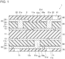
- the insulating layer 51 of the second buildup layer 50 corresponds to the insulating layer 21 of the first buildup layer 20, the via conductor 52 of the second buildup layer 50 corresponds to the via conductor 22 of the first buildup layer 20, and the surface conductor layer 53 of the second buildup layer 50 corresponds to the surface conductor layer 23 of the first buildup layer 20.
- the insulating layer 51 includes a hole 51a corresponding to the hole 21a of the insulating layer 21, the surface conductor layer 53 includes a seed layer 54 corresponding to the seed layer 24 of the surface conductor layer 23, the surface conductor layer 53 includes a top layer 55 corresponding to the top layer 25 of the surface conductor layer 23, and the seed layer 54 includes an opening 54a corresponding to the opening 24a of the seed layer 24.
- the seed layer 54 includes a tapered portion surrounding the opening 54a and gradually decreased in thickness toward an edge of the opening.
- the solder resist layers 40 and 70 are stacked on respective surfaces of a stacked body including the first buildup layer 20, the core substrate 10, and the second buildup layer 50. That is, the first solder resist layer 40 covers the surface conductor layer 23 as well as the surface 21d of the insulating layer 21 on the side far from the core substrate 10. The second solder resist layer 70 covers the surface conductor layer 53 as well as a surface 51d of the insulating layer 51 on a side far from the core substrate 10.
- the first solder resist layer 40 includes at least one opening 41. Part of the surface conductor layer 23 is overlapped with the opening 41, and the surface conductor layer 23 includes a portion positioned inside the opening 41 and functioning as a terminal.
- the second solder resist layer 70 includes at least one opening 71. Part of the surface conductor layer 53 is overlapped with the opening 71, and the surface conductor layer 53 includes a portion positioned inside the opening 71 and functioning as a terminal.
- the stacked body 10A includes the core substrate 10 and a buildup precursor layer 20A stacked thereon.
- a buildup precursor layer 50A may be stacked on the core substrate 10 such that the buildup precursor layers 50A and 20A oppose each other to interpose the core substrate 10.
- the stacked body 10A includes the seed layer 54, the insulating layer 51, the core substrate 10, the insulating layer 21, and the seed layer 24, which are disposed in the mentioned order as illustrated in FIG. 6 .
- the buildup precursor layer 20A includes the insulating layer 21 and the seed layer 24.
- the buildup precursor layer 50A includes the insulating layer 51 and the seed layer 54.
- the seed layers 24 and 54 have not yet constituted any wiring pattern.
- the insulating layer 21 does not include the hole 21a, and the insulating layer 51 does not include the hole 51a.
- the seed layers 24 and 54 are exemplarily 3 ⁇ m or more and 18 ⁇ m or less in thickness.
- the insulating layer 21 is exemplarily 40 ⁇ m to 100 ⁇ m in thickness.
- the stacked body 10A is exemplarily prepared as in (1) or (2) described below.
- the seed layers 24 and 54 are exemplarily 2 ⁇ m or more and 17 ⁇ m or less in thickness.
- the stacked body 10A is set in a laser processing machine, and a mask 110 is set between a laser oscillator of the laser processing machine and the seed layer 24.
- the mask 110 includes at least one through-hole 111 having a circular shape and penetrating the mask 110.
- the through-hole 111 has a diameter exemplarily from 2 mm to 3 mm, and more specifically 2.4 mm.
- the laser processing machine is used to apply a laser beam 150 to the seed layer 24 through the through-hole 111.
- the seed layer 24 is provided with the opening 24a where the laser beam 150 is applied.
- the seed layer 24 has already been roughened as described above. The laser beam 150 is thus absorbed into the seed layer 24 without being reflected by the seed layer 24.
- the laser processing machine has output of the laser beam 150 exemplarily 10 mJ/shot to 20 mJ/shot, and more specifically 16 mJ/shot.
- the opening 24a has a diameter determined in accordance with the diameter of the through-hole 111 and the output of the laser beam 150. The longer the diameter of the through-hole 111 is, the longer the diameter of the opening 24a is. The higher the output of the laser beam 150 is, the longer the diameter of the opening 24a is.
- the opening 24a is formed to have 100 ⁇ m in diameter.
- the output of the laser beam 150 is also called power.
- Application of the laser beam 150 is stopped when the laser beam 150 reaches a surface of the insulating layer 21.
- a plurality of openings 24a is formed in the seed layer 24 by changing the application location of the laser beam 150.
- the mask 110 is replaced with a mask 120 to be set.
- the mask 120 includes at least one through-hole 121 having a circular shape and penetrating the mask 120.
- the through-hole 121 is shorter in diameter than the through-hole 111 in the mask 110.
- the diameter of the through-hole 121 is exemplarily 1/3 or more and 1/2 or less the diameter of the through-hole 111, and more specifically 1.1 mm.
- the laser processing machine is used to apply a laser beam 160 to the insulating layer 21 through the through-hole 121 and the opening 24a.
- the insulating layer 21 is thus provided with the circular hole 21a where the laser beam 160 is applied.
- Output of the laser beam 160 is exemplarily 1/15 or more and 1/8 or less the output of the laser beam 150 for formation of the opening 24a, and more specifically 1.8 mJ/shot.
- the hole 21a thus formed is shorter in diameter than the opening 24a.
- the diameter of the hole 21a is determined in accordance with the diameter of the through-hole 121 and the output of the laser beam 160. The longer the diameter of the through-hole 121 is, the longer the diameter of the hole 21a is.
- the hole 21a is formed to have 80 ⁇ m in diameter.
- the laser beam 160 is stopped when the laser beam 160 reaches a surface of the conductor layer 12.
- the laser beam 160 is incident on the surface of the conductor layer 12 for a short period immediately before application of the laser beam 160 is stopped.
- the surface of the conductor layer 12 is thus formed into the concave surface shape by the laser beam 160.
- the laser beam 150 is incident on the region around the opening 24a to form the tapered portion 24b in the region around the opening 24a.
- a plurality of holes 21a is formed in the insulating layer 21 by changing the application location of the laser beam 160.
- the opening 54a is then formed in the seed layer 54.
- the hole 51a is subsequently formed in the insulating layer 51.
- any smear in the holes 21a and 51a is then removed through plasma treatment, with use of an aqueous solution of permanganic acid, or the like. As illustrated in FIG. 11 , such desmearing treatment increases the diameter of the hole 21a to be equal to the diameter of the opening 24a as well as increases the diameter of the hole 51a to be equal to the diameter of the opening 54a.
- Plating treatment is subsequently applied to the stacked body 10A provided with the openings 24a and 54a and the holes 21a and 51a to obtain the via conductors 22 and 52 and metal plated layers 25A and 55A entirely on respective surfaces of the stacked body 10A as illustrated in FIG. 12 .
- the metal plated layers 25A and 55A and the seed layers 24 and 54 are then provided with a wiring pattern.
- resist is initially stacked on each of the metal plated layers 25A and 55A.
- the resist is exposed to be developed.
- the metal plated layers 25A and 55A and the seed layers 24 and 54 are etched with the resist functioning as a mask, the metal plated layers 25A and 55A and the seed layers 24 and 54 are formed to constitute a wiring pattern.
- the metal plated layer 25A still remaining corresponds to the top layer 25 constituting the wiring pattern, and the metal plated layer 55A still remaining corresponds to the top layer 55 constituting the wiring pattern.
- the first solder resist layer 40 is stacked on the insulating layer 21 and the top layer 25, and the second solder resist layer 70 is stacked on the insulating layer 51 and the top layer 55.
- the printed wiring board 1 is completed through the above processes.
- a printed wiring board includes a core substrate and a buildup layer stacked on the core substrate.
- the buildup layer includes an insulating layer stacked on the core substrate, a hole penetrating the insulating layer in a thickness direction, and a via conductor filled in the hole.
- the via conductor has a columnar shape.
- the hole includes an inner wall surface having unevenness.
- the via conductor is in contact with the inner wall surface.
- the buildup layer includes a surface conductor layer disposed on the insulating layer on a side far from the core substrate.
- the via conductor includes a side surface directed toward an inner wall surface of the hole.
- the side surface includes at least one protrusion. The protrusion is inclined to be directed toward the surface conductor layer.
- the protrusion is inclined to be directed toward the core substrate.
- the surface conductor layer includes a seed layer and a top layer.
- the seed layer is positioned adjacent to the insulating layer, and includes an opening positioned to be overlapped with the via conductor.
- the opening includes an inner edge positioned to be overlapped with an open edge of the hole or positioned outside the open edge of the hole.
- the inner edge of the opening defines a region including a tapered portion gradually decreased in thickness toward the open edge.
- the core substrate includes a conductor layer on a surface in contact with the buildup layer.
- the conductor layer includes a portion being in contact with the via conductor and having a concave surface shape.
- a method of manufacturing a printed wiring board includes: preparing a stacked body including a core substrate and a buildup precursor layer that includes an insulating layer and a seed layer made of a metal in a mentioned order and that is overlapped with the core substrate; disposing, above and adjacent to the seed layer in the stacked body, a first mask including a first through-hole, and applying a first laser beam to the seed layer through the first through-hole to form an opening in the seed layer; disposing, on the seed layer at a position above the first through-hole, a second mask including a second through-hole smaller in diameter than the first through-hole, and applying a second laser beam to the insulating layer through the opening to form a hole in the insulating layer; and applying plating treatment to the insulating layer provided with the hole to grow a plated film on the seed layer and the hole and form a via conductor and a top layer.
- the second through-hole is 1/3 or more and 1/2 or less the first through-hole in diameter.
- output of the second laser beam is 1/15 or more and 1/8 or less output of the first laser beam.
- the method further includes increasing a diameter of the hole so as not to exceed an inner edge of the opening in the seed layer.
Landscapes
- Engineering & Computer Science (AREA)
- Manufacturing & Machinery (AREA)
- Microelectronics & Electronic Packaging (AREA)
- Production Of Multi-Layered Print Wiring Board (AREA)
- Printing Elements For Providing Electric Connections Between Printed Circuits (AREA)
Applications Claiming Priority (2)
| Application Number | Priority Date | Filing Date | Title |
|---|---|---|---|
| JP2022137463 | 2022-08-31 | ||
| PCT/JP2023/031794 WO2024048713A1 (ja) | 2022-08-31 | 2023-08-31 | 印刷配線板及びその製造方法 |
Publications (1)
| Publication Number | Publication Date |
|---|---|
| EP4583645A1 true EP4583645A1 (en) | 2025-07-09 |
Family
ID=90099810
Family Applications (1)
| Application Number | Title | Priority Date | Filing Date |
|---|---|---|---|
| EP23860475.5A Withdrawn EP4583645A1 (en) | 2022-08-31 | 2023-08-31 | Printed wiring board and method for manufacturing same |
Country Status (4)
| Country | Link |
|---|---|
| EP (1) | EP4583645A1 (https=) |
| JP (2) | JP7583228B2 (https=) |
| CN (1) | CN119732185A (https=) |
| WO (1) | WO2024048713A1 (https=) |
Family Cites Families (8)
| Publication number | Priority date | Publication date | Assignee | Title |
|---|---|---|---|---|
| JP3978152B2 (ja) * | 2003-05-19 | 2007-09-19 | 住友重機械工業株式会社 | レーザ加工方法 |
| JP4457843B2 (ja) * | 2004-10-15 | 2010-04-28 | 住友ベークライト株式会社 | 回路基板の製造方法 |
| KR20090110596A (ko) * | 2008-04-18 | 2009-10-22 | 삼성전기주식회사 | 인쇄회로기판 및 그 제조방법 |
| WO2010024233A1 (ja) * | 2008-08-27 | 2010-03-04 | 日本電気株式会社 | 機能素子を内蔵可能な配線基板及びその製造方法 |
| US8933556B2 (en) * | 2010-01-22 | 2015-01-13 | Ibiden Co., Ltd. | Wiring board |
| JP2014075523A (ja) * | 2012-10-05 | 2014-04-24 | Sumitomo Electric Printed Circuit Inc | プリント配線板及びその製造方法 |
| JP6846862B2 (ja) | 2015-10-26 | 2021-03-24 | 京セラ株式会社 | 印刷配線板およびその製造方法 |
| JP2021111711A (ja) * | 2020-01-10 | 2021-08-02 | 住友電工プリントサーキット株式会社 | フレキシブルプリント配線板及びその製造方法 |
-
2023
- 2023-08-31 CN CN202380062778.2A patent/CN119732185A/zh not_active Withdrawn
- 2023-08-31 EP EP23860475.5A patent/EP4583645A1/en not_active Withdrawn
- 2023-08-31 JP JP2024540014A patent/JP7583228B2/ja active Active
- 2023-08-31 WO PCT/JP2023/031794 patent/WO2024048713A1/ja not_active Ceased
-
2024
- 2024-10-31 JP JP2024191441A patent/JP2025017372A/ja active Pending
Also Published As
| Publication number | Publication date |
|---|---|
| JPWO2024048713A1 (https=) | 2024-03-07 |
| CN119732185A (zh) | 2025-03-28 |
| JP7583228B2 (ja) | 2024-11-13 |
| JP2025017372A (ja) | 2025-02-05 |
| WO2024048713A1 (ja) | 2024-03-07 |
Similar Documents
| Publication | Publication Date | Title |
|---|---|---|
| US6531661B2 (en) | Multilayer printed circuit board and method of making the same | |
| US8027169B2 (en) | Multilayer printed wiring board for semiconductor devices and method for manufacturing the board | |
| US8580066B2 (en) | Method for manufacturing multilayer wiring substrate | |
| US8093503B2 (en) | Multilayer wiring board | |
| JP4331769B2 (ja) | 配線構造及びその形成方法並びにプリント配線板 | |
| KR101472633B1 (ko) | 하이브리드 적층기판, 그 제조방법 및 패키지 기판 | |
| JP5566720B2 (ja) | 多層配線基板及びその製造方法 | |
| KR101167466B1 (ko) | 다층 인쇄회로기판 그 제조방법 | |
| US20150027758A1 (en) | Multilayer wiring substrate and manufacturing method therefor | |
| JP2017143254A (ja) | 積層埋込キャパシタを有する配線基板及びその製造方法 | |
| JP5284146B2 (ja) | 多層配線基板、及びその製造方法 | |
| US20120097319A1 (en) | Method of manufacturing multilayer wiring substrate | |
| KR102561794B1 (ko) | 인쇄회로기판 및 이의 제조 방법 | |
| US20150313018A1 (en) | Wiring substrate and production method therefor | |
| KR101579019B1 (ko) | 다층배선기판 | |
| US20090289030A1 (en) | Method of fabricating printed wiring board | |
| EP4583645A1 (en) | Printed wiring board and method for manufacturing same | |
| JP2017084914A (ja) | 印刷配線板およびその製造方法 | |
| US20180156841A1 (en) | Structure and Method of Making Circuitized Substrate Assembly | |
| US20250300052A1 (en) | Semiconductor package and fabricating method thereof | |
| JP2009200151A (ja) | 回路基板及びその製造方法 | |
| TW202335542A (zh) | 印刷電路板及其製造方法 | |
| JP2024117490A (ja) | 導波路基板及び導波路基板の製造方法 | |
| US20250096105A1 (en) | Package substrate and fabricating method thereof | |
| JP2023178076A (ja) | 配線基板、半導体装置及び配線基板の製造方法 |
Legal Events
| Date | Code | Title | Description |
|---|---|---|---|
| STAA | Information on the status of an ep patent application or granted ep patent |
Free format text: STATUS: THE INTERNATIONAL PUBLICATION HAS BEEN MADE |
|
| PUAI | Public reference made under article 153(3) epc to a published international application that has entered the european phase |
Free format text: ORIGINAL CODE: 0009012 |
|
| STAA | Information on the status of an ep patent application or granted ep patent |
Free format text: STATUS: REQUEST FOR EXAMINATION WAS MADE |
|
| 17P | Request for examination filed |
Effective date: 20250227 |
|
| AK | Designated contracting states |
Kind code of ref document: A1 Designated state(s): AL AT BE BG CH CY CZ DE DK EE ES FI FR GB GR HR HU IE IS IT LI LT LU LV MC ME MK MT NL NO PL PT RO RS SE SI SK SM TR |
|
| DAV | Request for validation of the european patent (deleted) | ||
| DAX | Request for extension of the european patent (deleted) | ||
| STAA | Information on the status of an ep patent application or granted ep patent |
Free format text: STATUS: THE APPLICATION HAS BEEN WITHDRAWN |
|
| 18W | Application withdrawn |
Effective date: 20251229 |