WO2024029385A1 - 半導体装置 - Google Patents
半導体装置 Download PDFInfo
- Publication number
- WO2024029385A1 WO2024029385A1 PCT/JP2023/027007 JP2023027007W WO2024029385A1 WO 2024029385 A1 WO2024029385 A1 WO 2024029385A1 JP 2023027007 W JP2023027007 W JP 2023027007W WO 2024029385 A1 WO2024029385 A1 WO 2024029385A1
- Authority
- WO
- WIPO (PCT)
- Prior art keywords
- metal layer
- conductive member
- semiconductor device
- layer
- semiconductor
- Prior art date
Links
- 239000004065 semiconductor Substances 0.000 title claims abstract description 257
- 229910052751 metal Inorganic materials 0.000 claims abstract description 184
- 239000002184 metal Substances 0.000 claims abstract description 184
- 229920005989 resin Polymers 0.000 claims abstract description 101
- 239000011347 resin Substances 0.000 claims abstract description 101
- 238000007789 sealing Methods 0.000 claims abstract description 34
- 229910000679 solder Inorganic materials 0.000 claims abstract description 19
- 229910052709 silver Inorganic materials 0.000 claims description 32
- 229910052802 copper Inorganic materials 0.000 claims description 14
- 239000010410 layer Substances 0.000 description 265
- 239000004332 silver Substances 0.000 description 28
- 239000010949 copper Substances 0.000 description 22
- 230000004888 barrier function Effects 0.000 description 21
- 238000007747 plating Methods 0.000 description 20
- 230000004907 flux Effects 0.000 description 17
- 230000005855 radiation Effects 0.000 description 15
- 239000000463 material Substances 0.000 description 13
- 230000004048 modification Effects 0.000 description 11
- 238000012986 modification Methods 0.000 description 11
- RYGMFSIKBFXOCR-UHFFFAOYSA-N Copper Chemical compound [Cu] RYGMFSIKBFXOCR-UHFFFAOYSA-N 0.000 description 10
- 239000004020 conductor Substances 0.000 description 8
- NRTOMJZYCJJWKI-UHFFFAOYSA-N Titanium nitride Chemical compound [Ti]#N NRTOMJZYCJJWKI-UHFFFAOYSA-N 0.000 description 6
- 230000017525 heat dissipation Effects 0.000 description 6
- PXHVJJICTQNCMI-UHFFFAOYSA-N nickel Substances [Ni] PXHVJJICTQNCMI-UHFFFAOYSA-N 0.000 description 6
- 229910052782 aluminium Inorganic materials 0.000 description 4
- XAGFODPZIPBFFR-UHFFFAOYSA-N aluminium Chemical compound [Al] XAGFODPZIPBFFR-UHFFFAOYSA-N 0.000 description 4
- 239000010936 titanium Substances 0.000 description 4
- 230000001052 transient effect Effects 0.000 description 4
- 239000002344 surface layer Substances 0.000 description 3
- 229910002601 GaN Inorganic materials 0.000 description 2
- JMASRVWKEDWRBT-UHFFFAOYSA-N Gallium nitride Chemical compound [Ga]#N JMASRVWKEDWRBT-UHFFFAOYSA-N 0.000 description 2
- RTAQQCXQSZGOHL-UHFFFAOYSA-N Titanium Chemical compound [Ti] RTAQQCXQSZGOHL-UHFFFAOYSA-N 0.000 description 2
- 238000009792 diffusion process Methods 0.000 description 2
- 239000010931 gold Substances 0.000 description 2
- 230000020169 heat generation Effects 0.000 description 2
- 238000000034 method Methods 0.000 description 2
- 229910052759 nickel Inorganic materials 0.000 description 2
- 230000001737 promoting effect Effects 0.000 description 2
- 230000000630 rising effect Effects 0.000 description 2
- HBMJWWWQQXIZIP-UHFFFAOYSA-N silicon carbide Chemical compound [Si+]#[C-] HBMJWWWQQXIZIP-UHFFFAOYSA-N 0.000 description 2
- 229910010271 silicon carbide Inorganic materials 0.000 description 2
- 238000005245 sintering Methods 0.000 description 2
- 239000007790 solid phase Substances 0.000 description 2
- 238000004544 sputter deposition Methods 0.000 description 2
- 229910052719 titanium Inorganic materials 0.000 description 2
- 230000015572 biosynthetic process Effects 0.000 description 1
- 238000006243 chemical reaction Methods 0.000 description 1
- 230000000694 effects Effects 0.000 description 1
- 238000010292 electrical insulation Methods 0.000 description 1
- 239000003822 epoxy resin Substances 0.000 description 1
- 230000005669 field effect Effects 0.000 description 1
- 239000000945 filler Substances 0.000 description 1
- PCHJSUWPFVWCPO-UHFFFAOYSA-N gold Chemical compound [Au] PCHJSUWPFVWCPO-UHFFFAOYSA-N 0.000 description 1
- 229910052737 gold Inorganic materials 0.000 description 1
- 239000011159 matrix material Substances 0.000 description 1
- 229920000647 polyepoxide Polymers 0.000 description 1
- 229910052710 silicon Inorganic materials 0.000 description 1
- 239000010703 silicon Substances 0.000 description 1
Images


Classifications
-
- H—ELECTRICITY
- H01—ELECTRIC ELEMENTS
- H01L—SEMICONDUCTOR DEVICES NOT COVERED BY CLASS H10
- H01L21/00—Processes or apparatus adapted for the manufacture or treatment of semiconductor or solid state devices or of parts thereof
- H01L21/02—Manufacture or treatment of semiconductor devices or of parts thereof
- H01L21/04—Manufacture or treatment of semiconductor devices or of parts thereof the devices having potential barriers, e.g. a PN junction, depletion layer or carrier concentration layer
- H01L21/50—Assembly of semiconductor devices using processes or apparatus not provided for in a single one of the subgroups H01L21/06 - H01L21/326, e.g. sealing of a cap to a base of a container
- H01L21/60—Attaching or detaching leads or other conductive members, to be used for carrying current to or from the device in operation
-
- H—ELECTRICITY
- H01—ELECTRIC ELEMENTS
- H01L—SEMICONDUCTOR DEVICES NOT COVERED BY CLASS H10
- H01L23/00—Details of semiconductor or other solid state devices
- H01L23/28—Encapsulations, e.g. encapsulating layers, coatings, e.g. for protection
- H01L23/29—Encapsulations, e.g. encapsulating layers, coatings, e.g. for protection characterised by the material, e.g. carbon
-
- H—ELECTRICITY
- H01—ELECTRIC ELEMENTS
- H01L—SEMICONDUCTOR DEVICES NOT COVERED BY CLASS H10
- H01L23/00—Details of semiconductor or other solid state devices
- H01L23/34—Arrangements for cooling, heating, ventilating or temperature compensation ; Temperature sensing arrangements
- H01L23/36—Selection of materials, or shaping, to facilitate cooling or heating, e.g. heatsinks
- H01L23/373—Cooling facilitated by selection of materials for the device or materials for thermal expansion adaptation, e.g. carbon
-
- H—ELECTRICITY
- H01—ELECTRIC ELEMENTS
- H01L—SEMICONDUCTOR DEVICES NOT COVERED BY CLASS H10
- H01L25/00—Assemblies consisting of a plurality of individual semiconductor or other solid state devices ; Multistep manufacturing processes thereof
- H01L25/03—Assemblies consisting of a plurality of individual semiconductor or other solid state devices ; Multistep manufacturing processes thereof all the devices being of a type provided for in the same subgroup of groups H01L27/00 - H01L33/00, or in a single subclass of H10K, H10N, e.g. assemblies of rectifier diodes
- H01L25/04—Assemblies consisting of a plurality of individual semiconductor or other solid state devices ; Multistep manufacturing processes thereof all the devices being of a type provided for in the same subgroup of groups H01L27/00 - H01L33/00, or in a single subclass of H10K, H10N, e.g. assemblies of rectifier diodes the devices not having separate containers
- H01L25/07—Assemblies consisting of a plurality of individual semiconductor or other solid state devices ; Multistep manufacturing processes thereof all the devices being of a type provided for in the same subgroup of groups H01L27/00 - H01L33/00, or in a single subclass of H10K, H10N, e.g. assemblies of rectifier diodes the devices not having separate containers the devices being of a type provided for in group H01L29/00
-
- H—ELECTRICITY
- H01—ELECTRIC ELEMENTS
- H01L—SEMICONDUCTOR DEVICES NOT COVERED BY CLASS H10
- H01L25/00—Assemblies consisting of a plurality of individual semiconductor or other solid state devices ; Multistep manufacturing processes thereof
- H01L25/18—Assemblies consisting of a plurality of individual semiconductor or other solid state devices ; Multistep manufacturing processes thereof the devices being of types provided for in two or more different subgroups of the same main group of groups H01L27/00 - H01L33/00, or in a single subclass of H10K, H10N
Definitions
- the present disclosure relates to a semiconductor device.
- Patent Document 1 discloses an example of a conventional semiconductor device.
- the semiconductor device disclosed in the document includes a conductor, a semiconductor element, a conductive member, and a sealing resin.
- a semiconductor element is mounted on a conductor.
- a semiconductor element has an electrode.
- a conductive member is connected to this electrode via solder.
- the sealing resin covers at least a portion of each of the conductor, the semiconductor element, and the conductive member.
- the semiconductor element When a semiconductor device is in operation, the semiconductor element repeatedly generates heat. A portion of the heat generated in the semiconductor layer of the semiconductor element is radiated through the solder and the conductive member. If the amount of heat transfer (heat flux) per unit time from the semiconductor layer of the semiconductor element to the solder is not sufficient, the temperature of the semiconductor element will rise transiently. This temperature increase may impair proper operation of the semiconductor device.
- An object of the present disclosure is to provide a semiconductor device that is improved over the conventional semiconductor device.
- one object of the present disclosure is to provide a semiconductor device that can operate a semiconductor element more appropriately.
- a semiconductor device includes: a semiconductor element having a semiconductor layer and a first electrode disposed on a first side in the thickness direction of the semiconductor layer; a first conductive member, a second conductive member joined to the semiconductor element from the second side in the thickness direction, a first resin surface facing the first side in the thickness direction, and a first resin surface facing the second side in the thickness direction; A sealing resin having two resin surfaces and covering the semiconductor element and at least a portion of each of the first conductive member and the second conductive member.
- the first electrode includes a first metal layer containing a metal having higher thermal conductivity than solder.
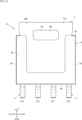
- FIG. 1 is a perspective view showing a semiconductor device according to a first embodiment of the present disclosure.
- FIG. 2 is a perspective view of main parts showing a semiconductor device according to a first embodiment of the present disclosure.
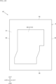
- FIG. 3 is a plan view showing a semiconductor device according to the first embodiment of the present disclosure.
- FIG. 4 is a plan view of main parts of a semiconductor device according to a first embodiment of the present disclosure.
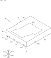
- FIG. 5 is a bottom view showing the semiconductor device according to the first embodiment of the present disclosure.
- FIG. 6 is a bottom view of essential parts of the semiconductor device according to the first embodiment of the present disclosure.
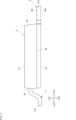
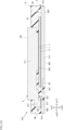
- FIG. 7 is a side view showing the semiconductor device according to the first embodiment of the present disclosure.
- FIG. 8 is a cross-sectional view taken along line VIII-VIII in FIG. 4.
- FIG. 9 is a sectional view taken along line IX-IX in FIG. 4.
- FIG. 10 is a cross-sectional view of a main part schematically showing a first embodiment of a junction structure included in a semiconductor device of the present disclosure.
- FIG. 11 is a cross-sectional view of a main part schematically showing an example of a bonding structure included in a semiconductor device according to a first embodiment of the present disclosure.
- FIG. 12 is a cross-sectional view of a main part schematically showing another example of the bonding structure included in the semiconductor device according to the first embodiment of the present disclosure.
- FIG. 13 is a cross-sectional view of a main part schematically showing another example of a bonding structure included in the semiconductor device according to the first embodiment of the present disclosure.
- FIG. 10 is a cross-sectional view of a main part schematically showing a first embodiment of a junction structure included in a semiconductor device of the present disclosure.
- FIG. 11 is a cross-sectional view of a main part
- FIG. 14 is a cross-sectional view of main parts schematically showing another example of a bonding structure included in the semiconductor device according to the first embodiment of the present disclosure.
- FIG. 15 is a cross-sectional view showing a first modification of the semiconductor device according to the first embodiment of the present disclosure.
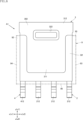
- FIG. 16 is a perspective view showing a semiconductor device according to a second embodiment of the present disclosure.
- FIG. 17 is a perspective view of essential parts showing a semiconductor device according to a second embodiment of the present disclosure.
- FIG. 18 is a plan view showing a semiconductor device according to a second embodiment of the present disclosure.
- FIG. 19 is a plan view of main parts showing a semiconductor device according to a second embodiment of the present disclosure.
- FIG. 19 is a plan view of main parts showing a semiconductor device according to a second embodiment of the present disclosure.
- FIG. 20 is a bottom view showing a semiconductor device according to a second embodiment of the present disclosure.
- FIG. 21 is a bottom view of essential parts showing a semiconductor device according to a second embodiment of the present disclosure.
- FIG. 22 is a cross-sectional view taken along line XXII-XXII in FIG. 21.
- FIG. 23 is a cross-sectional view taken along line XXIII-XXIII in FIG. 21.
- FIG. 24 is a cross-sectional view showing a first modification of the semiconductor device according to the second embodiment of the present disclosure.
- FIG. 25 is a cross-sectional view showing a second modification of the semiconductor device according to the second embodiment of the present disclosure.
- a thing A is formed on a thing B and "a thing A is formed on a thing B” mean “a thing A is formed on a thing B” unless otherwise specified.
- "something A is placed on something B” and “something A is placed on something B” mean "something A is placed on something B” unless otherwise specified.
- a certain surface A faces direction B means when the angle of the surface A with respect to the direction B is 90 degrees. This includes, but is not limited to, the case where the surface A is inclined with respect to the direction B.
- the semiconductor device A1 of this embodiment includes a semiconductor element 1, a first conductive member 2, a second conductive member 3, a third conductive member 4, a first bonding layer 7, a second bonding layer 8, and a sealing resin 9.
- the application of the semiconductor device A1 is not limited in any way, and is used, for example, in electronic equipment including a power conversion circuit, such as a DC-DC converter.
- FIG. 1 is a perspective view showing a semiconductor device A1.
- FIG. 2 is a perspective view of essential parts of the semiconductor device A1.
- FIG. 3 is a plan view showing the semiconductor device A1.
- FIG. 4 is a plan view of essential parts of the semiconductor device A1.
- FIG. 5 is a bottom view showing the semiconductor device A1.
- FIG. 6 is a bottom view of essential parts of the semiconductor device A1.
- FIG. 7 is a side view showing the semiconductor device A1.
- FIG. 8 is a cross-sectional view taken along line VIII-VIII in FIG. 4.
- FIG. 9 is a sectional view taken along line IX-IX in FIG. 4.
- FIG. 10 is a cross-sectional view of a main part schematically showing an example of a bonding structure included in the semiconductor device A1.
- the thickness direction of the present disclosure is defined as the thickness direction z.
- the first side in the thickness direction z is referred to as the z1 side, and the second side opposite to the first side in the z direction is referred to as the z2 side.
- one direction perpendicular to the thickness direction z is defined as a first direction x.
- the first side in the first direction x is referred to as the x1 side, and the second side opposite to the x1 side is referred to as the x2 side.
- a direction perpendicular to the thickness direction z and the first direction x is defined as a second direction y.
- the first side in the second direction y is referred to as the y1 side, and the second side opposite to the y1 side is referred to as the y2 side.
- the semiconductor element 1 is, for example, a MOSFET (Metal-Oxide-Semiconductor Field-Effect Transistor).
- the semiconductor element 1 may be a switching element such as an IGBT (Insulated Gate Bipolar Transistor) or a diode.
- IGBT Insulated Gate Bipolar Transistor
- the semiconductor element 1 is an n-channel type MOSFET with a vertical structure.
- the semiconductor element 1 has a semiconductor layer 10, a first electrode 11, a second electrode 12, and a third electrode 13, as shown in FIGS. 2, 4, and 8 to 10.
- FIG. 10 schematically shows a junction structure B1 included in a semiconductor device A1.
- the bonded structure B1 has a structure in which the semiconductor element 1, the first conductive member 2, the second conductive member 3, the first bonding layer 7, and the second bonding layer 8 are bonded to each other.
- the first conductive member 2 and the second conductive member 3 are shown protruding from the semiconductor element 1 in a plane including the first direction x and the second direction y.
- the fifth conductive member 6 and the first bonding layer 7 are shown to have a trapezoidal cross section that joins the semiconductor element 1 and the first conductive member 2 or the second conductive member 3.
- the semiconductor layer 10 is a layer containing a semiconductor.
- the composition of the semiconductor includes, for example, Si (silicon), SiC (silicon carbide), and the like. Further, unlike this embodiment, when the semiconductor element 1 is a switching element with a horizontal structure, the semiconductor layer 10 includes, for example, GaN (gallium nitride).
- the first electrode 11 is arranged on the z1 side of the semiconductor layer 10 in the thickness direction z. A current corresponding to the power converted by the semiconductor element 1 flows through the first electrode 11 . That is, the first electrode 11 corresponds to the source electrode of the semiconductor element 1.
- the second electrode 12 is arranged on the z2 side of the semiconductor layer 10 in the thickness direction z. A current corresponding to the power before being converted by the semiconductor element 1 flows through the second electrode 12 . That is, the second electrode 12 corresponds to the drain electrode of the semiconductor element 1.
- the third electrode 13 is arranged on the same z1 side as the first electrode 11 in the thickness direction z.
- a gate voltage for driving the semiconductor element 1 is applied to the third electrode 13 . That is, the third electrode 13 corresponds to the gate electrode of the semiconductor element 1.
- the area of the third electrode 13 is smaller than the area of the first electrode 11 when viewed in the thickness direction z.
- the first electrode 11 includes a first metal layer 111, a second metal layer 112, a first intermediate metal layer 113, and a first barrier metal layer 114.
- the first metal layer 111 includes a metal having higher thermal conductivity than solder.
- the first metal layer 111 contains a metal having higher thermal conductivity than solder as a main component.
- the first metal layer 111 contains, for example, Ag (silver) or Cu (copper). In the following description, the case where the first metal layer 111 has Ag (silver) as a main component will be described as an example.
- the first metal layer 111 mainly composed of Ag (silver) include an Ag (silver) sintered layer, an Ag (silver) paste layer, and an Ag (silver) formed by a film formation technique such as sputtering. layer, Ag (silver) plating layer, etc.
- the first metal layer 111 forms the surface layer of the first electrode 11 .
- the second metal layer 112 is interposed between the semiconductor layer 10 and the first metal layer 111.
- the second metal layer 112 is a layer containing Al (aluminum), for example.
- the thickness t111 of the first metal layer 111 and the thickness t112 of the second metal layer 112 are not limited at all.
- the thickness t111 is thicker than the thickness t112.
- the thickness t111 is, for example, 5 ⁇ m or more and 40 ⁇ m or less.
- the thickness t112 is, for example, 2 ⁇ m or more and 8 ⁇ m or less.
- the first intermediate metal layer 113 is interposed between the first metal layer 111 and the second metal layer 112.
- the first intermediate metal layer 113 contains, for example, Ti (titanium), Ni (nickel), or the like.
- the thickness of the first intermediate metal layer 113 is, for example, 0.1 ⁇ m or more and 0.6 ⁇ m or less.
- the first intermediate metal layer 113 is a layer for suppressing damage to the second metal layer 112 when forming the first metal layer 111 on the second metal layer 112, for example.
- the first barrier metal layer 114 is interposed between the second metal layer 112 and the semiconductor layer 10.
- the first barrier metal layer 114 includes, for example, TiN (titanium nitride).
- the thickness of the first barrier metal layer 114 is, for example, 0.01 ⁇ m or more and 0.1 ⁇ m or less.
- the first barrier metal layer 114 is a layer for suppressing damage to the semiconductor layer 10 when forming the second metal layer 112 on the semiconductor layer 10, for example.
- the second electrode 12 of this embodiment includes a fourth metal layer 122 and a second barrier metal layer 124.
- the fourth metal layer 122 is a layer containing Al (aluminum), for example.
- the fourth metal layer 122 forms the surface layer of the second electrode 12.
- the thickness of the fourth metal layer 122 is not limited at all, and may be the same as or different from the thickness t112 of the second metal layer 112.
- the second barrier metal layer 124 is interposed between the fourth metal layer 122 and the semiconductor layer 10.
- the second barrier metal layer 124 includes, for example, TiN (titanium nitride).
- the thickness of the second barrier metal layer 124 is, for example, 0.01 ⁇ m or more and 0.1 ⁇ m or less.
- the second barrier metal layer 124 is a layer for suppressing damage to the semiconductor layer 10 when forming the fourth metal layer 122 on the semiconductor layer 10, for example.
- the first conductive member 2 includes a portion disposed on the z1 side in the thickness direction z with respect to the semiconductor element 1.
- the first conductive member 2 includes a conductive material such as metal, and includes Cu (copper), for example.
- the first conductive member 2 has a first main surface 201 and a second main surface 202, as shown in FIGS. 1 to 10.
- the first main surface 201 is a surface facing the z1 side in the thickness direction z.
- the second main surface 202 is a surface facing the z2 side in the thickness direction z.
- the semiconductor element 1 is electrically connected to the second main surface 202 .
- the first main surface 201 is covered with the sealing resin 9 in this example.
- the first conductive member 2 has a first island portion 211, a plurality of first terminal portions 212, and a recessed portion 221, as shown in FIGS. 1 to 9.
- the first island portion 211 is a portion that is conductively bonded to the semiconductor element 1.
- the first island portion 211 includes a part of the first main surface 201 and a part of the second main surface 202.
- the shape and size of the first island portion 211 are not limited in any way, and in the illustrated example, it has a shape that overlaps all of the first electrode 11 when viewed in the thickness direction z, and also overlaps the third electrode 13. It has an exposed shape.
- the plurality of first terminal portions 212 are connected to the first island portion 211 on the y2 side in the second direction y.
- the plurality of first terminal parts 212 each extend in the second direction y when viewed in the thickness direction z, and are arranged at intervals in the first direction x.
- the number of the plurality of first terminal sections 212 is not limited at all, and may be three as in the illustrated example, two, or four or more. Alternatively, a configuration including only one first terminal portion 212 may be used.
- the first terminal portion 212 is connected to the first island portion 211 and covered with the sealing resin 9, and extends from the sealing resin 9 to the y2 side in the second direction y.
- the plurality of first terminal parts 212 are used as terminals when mounting the semiconductor device A1.
- the recessed portion 221 is a portion recessed from the first main surface 201 toward the z2 side in the thickness direction z.
- the recessed portion 221 overlaps the first island portion 211 when viewed in the thickness direction z.
- the first conductive member 2 includes a first base material 21 and a first plating layer 22.
- the first base material 21 is a main portion of the first conductive member 2, and includes, for example, Cu (copper).
- the first plating layer 22 is formed at a proper location on the first base material 21 and contains, for example, Ag (silver).
- the first plating layer 22 is provided at least at a location that is bonded to the semiconductor element 1 by the first bonding layer 7 .
- the first bonding layer 7 electrically connects the first electrode 11 of the semiconductor element 1 and the second main surface 202 of the first conductive member 2 .
- the first bonding layer 7 electrically connects the first metal layer 111 and the first plating layer 22.
- the specific structure of the first bonding layer 7 is not limited at all, and is made of, for example, a conductive bonding material such as solder or Ag (silver) plating.
- the thickness t7 of the first bonding layer 7 is not limited at all, and in this embodiment, it is thinner than the thickness t111 of the first metal layer 111.
- the thickness t7 is, for example, 4 ⁇ m or more and 30 ⁇ m or less.
- the second conductive member 3 is arranged on the z2 side in the thickness direction z with respect to the semiconductor element 1.
- the second conductive member 3 includes a conductive material such as metal, and includes Cu (copper), for example.
- the second conductive member 3 has a third main surface 301 and a fourth main surface 302, as shown in FIGS. 1 to 10.
- the third main surface 301 is a surface facing the z1 side in the thickness direction z.
- the fourth main surface 302 is a surface facing the z2 side in the thickness direction z.
- the semiconductor element 1 is mounted on the third main surface 301. As shown in FIGS. 5 and 6, the fourth main surface 302 is exposed from the sealing resin 9.
- the second conductive member 3 has a second island portion 311, a second terminal portion 312, a thin extension portion 321, and a through hole 322, as shown in FIGS. 1 to 9.
- the second island portion 311 is a portion on which all or a portion of the semiconductor element 1 is mounted.
- the second island portion 311 includes a part of the third main surface 301 and a part of the fourth main surface 302.
- the shape and size of the second island portion 311 are not limited in any way, and in the illustrated example, it has a substantially rectangular shape when viewed in the thickness direction z.
- the second terminal portion 312 is a portion connected to the second island portion 311 on the y1 side in the second direction y.
- the second terminal portion 312 includes a part of the third main surface 301 and a part of the fourth main surface 302.
- the second terminal portion 312 may be used as a terminal when mounting the semiconductor device A1.
- the thin extension portion 321 is a portion that includes the third main surface 301 and does not include the fourth main surface 302.
- the thickness of the thin extension portion 321 in the thickness direction z is thinner than the thickness of the second island portion 311 in the thickness direction z.
- the thin extension portion 321 extends from the second island portion 311 .
- the thin extension portion 321 extends from the second island portion 311 to the x1 side and the x2 side in the first direction x, and to the y2 side in the second direction y.
- the through hole 322 penetrates the second conductive member 3 in the thickness direction z.
- the through hole 322 is partially filled with the sealing resin 9.
- the size of the cross section of the through hole 322 perpendicular to the thickness direction z is larger on the z2 side than on the z1 side in the thickness direction z. This has the effect of suppressing, for example, the second conductive member 3 from falling off from the sealing resin 9.
- the second conductive member 3 includes a second base material 31 and a second plating layer 32.
- the second base material 31 is a main portion of the second conductive member 3, and includes, for example, Cu (copper).
- the second plating layer 32 is formed at a suitable location on the second base material 31 and contains, for example, Ag (silver).
- the second plating layer 32 is provided at least at a location where it is bonded to the semiconductor element 1 by the second bonding layer 8 .
- the second bonding layer 8 electrically connects the second electrode 12 of the semiconductor element 1 and the third main surface 301 of the second conductive member 3 .
- the second bonding layer 8 electrically connects the fourth metal layer 122 and the second plating layer 32.
- the specific structure of the second bonding layer 8 is not limited at all, and is made of, for example, a conductive bonding material such as solder or Ag (silver) plating. Note that, unlike this embodiment, when the semiconductor element 1 does not include the second electrode 12 on the z2 side in the thickness direction z, the second bonding layer 8 simply bonds the semiconductor element 1 and the second conductive member 3. However, a configuration may be adopted in which they are not electrically connected to each other.
- the third conductive member 4 includes a portion disposed on the z1 side in the thickness direction z with respect to the semiconductor element 1.
- the third conductive member 4 includes a conductive material such as metal, and includes Cu (copper), for example.
- the third conductive member 4 has a pad portion 411 and a third terminal portion 412, as shown in FIGS. 2 to 7.
- the pad portion 411 is a portion electrically connected to the third electrode 13 of the semiconductor element 1.
- the shape and size of the pad portion 411 are not limited in any way, and in the illustrated example, the pad portion 411 has a shape that overlaps a part of the third electrode 13 when viewed in the thickness direction z.
- the pad portion 411 is electrically connected to the third electrode 13 by solder or the like (not shown).
- the third terminal portion 412 is connected to the pad portion 411 on the y2 side in the second direction y.
- the third terminal portion 412 extends in the second direction y when viewed in the thickness direction z.
- the third terminal portion 412 is a portion connected to the pad portion 411 and covered with the sealing resin 9, and protrudes from the sealing resin 9 toward the y2 side in the second direction y. a portion folded back on the z2 side in the thickness direction z, and a portion located on the z2 side in the thickness direction z.
- the third terminal portion 412 has a shape and size that generally overlaps with the first terminal portion 212 when viewed in the first direction x.
- the third terminal portion 412 is used as a terminal when mounting the semiconductor device A1.
- the sealing resin 9 covers the semiconductor element 1 and a portion of each of the first conductive member 2, the second conductive member 3, and the third conductive member 4.
- the sealing resin 9 has electrical insulation properties.
- the sealing resin 9 includes, for example, a black epoxy resin containing filler.
- the shape of the sealing resin 9 is not limited at all. As shown in FIGS. 1 to 9, the sealing resin 9 of this embodiment has a first resin surface 91, a second resin surface 92, a third resin surface 93, a fourth resin surface 94, a fifth resin surface 95, and It has a sixth resin surface 96.
- the first resin surface 91 is a surface facing the z1 side in the thickness direction z.
- the second resin surface 92 is a surface facing the z2 side in the thickness direction z.
- the fourth main surface 302 of the second conductive member 3 is exposed from the second resin surface 92 .
- the first resin surface 91 and the second resin surface 92 are flat surfaces, but are not limited to this, and may be, for example, curved surfaces or bent surfaces.
- the second resin surface 92 and the fourth main surface 302 are flush with each other.
- the third resin surface 93 is a surface facing the x1 side in the first direction x.
- the fourth resin surface 94 is a surface facing the x2 side in the first direction x.
- the third resin surface 93 and the fourth resin surface 94 are slightly curved surfaces, but are not limited to this, and may be curved surfaces, flat surfaces, etc., for example.
- the fifth resin surface 95 is a surface facing the y1 side in the second direction y.
- the sixth resin surface 96 is a surface facing the y2 side in the second direction y.
- the fifth resin surface 95 and the sixth resin surface 96 are slightly curved surfaces, but are not limited to this, and may be curved surfaces, flat surfaces, etc., for example.
- a plurality of first terminal portions 212 and third terminal portions 412 protrude from the sixth resin surface 96 .
- the first electrode 11 includes a first metal layer 111.
- the first metal layer 111 includes a metal having higher thermal conductivity than solder.
- the semiconductor element 1 is a switching element with a vertical structure
- heat generation becomes significant in a portion of the semiconductor layer 10 located on the z1 side in the thickness direction z. It is reasonable to provide the first metal layer 111 as a measure to suppress the temperature rise due to such a tendency of heat generation.
- the heat flux of heat radiation from the semiconductor layer 10 can be further increased. It is preferable that the first metal layer 111 has Ag (silver) as a main component in order to increase heat flux.
- the configuration in which the first metal layer 111 is, for example, a sintered Ag (silver) layer is suitable for finishing the first metal layer 111 into a desired shape and thickness.
- the thickness t111 of the first metal layer 111 is thicker than the thickness t112 of the second metal layer 112. Thereby, heat from the semiconductor layer 10 can be more quickly transmitted to the first metal layer 111 via the second metal layer 112. Further, the thickness t7 of the first bonding layer 7 is thinner than the thickness t111 of the first metal layer 111. This allows the heat transferred to the first metal layer 111 to be transferred to the first conductive member 2 more efficiently, which is preferable for promoting heat dissipation from the semiconductor layer 10.
- FIG. 11 to 14 schematically show other examples of the bonding structure included in the semiconductor device A1.
- Various bonding structures including the bonding structure B1 described above and bonding structures B2 to B5 described below can be appropriately employed in various semiconductor devices including the semiconductor device A1 and the semiconductor device described below.
- the bonded structure B2 shown in FIG. 11 differs from the bonded structure B1 described above mainly in the configuration of the second electrode 12.
- the second electrode 12 of this example includes a third metal layer 121, a fourth metal layer 122, a second intermediate metal layer 123, and a second barrier metal layer 124.
- the third metal layer 121 includes a metal having higher thermal conductivity than solder.
- the third metal layer 121 contains a metal having higher thermal conductivity than solder as a main component.
- the third metal layer 121 contains, for example, Ag (silver) or Cu (copper). In the following description, a case where the third metal layer 121 has Ag (silver) as a main component will be described as an example.
- the third metal layer 121 containing Ag (silver) as a main component include, for example, an Ag (silver) sintered layer, an Ag (silver) paste layer, and an Ag (silver) formed by a film forming technique such as sputtering. layer, Ag (silver) plating layer, etc.
- the third metal layer 121 forms the surface layer of the second electrode 12 .
- the fourth metal layer 122 is interposed between the semiconductor layer 10 and the third metal layer 121.
- the fourth metal layer 122 is a layer containing Al (aluminum), for example.
- the thickness t121 of the third metal layer 121 and the thickness t122 of the fourth metal layer 122 are not limited at all. In this embodiment, the thickness t121 is thicker than the thickness t122.
- the thickness t121 is, for example, 5 ⁇ m or more and 10 ⁇ m or less.
- the thickness t122 is, for example, 2 ⁇ m or more and 8 ⁇ m or less.
- the second intermediate metal layer 123 is interposed between the third metal layer 121 and the fourth metal layer 122.
- the second intermediate metal layer 123 contains, for example, Ti (titanium), Ni (nickel), or the like.
- the thickness of the second intermediate metal layer 123 is, for example, 0.1 ⁇ m or more and 0.6 ⁇ m or less.
- the second intermediate metal layer 123 is a layer for suppressing damage to the fourth metal layer 122 when forming the third metal layer 121 on the fourth metal layer 122, for example.
- the second barrier metal layer 124 is interposed between the fourth metal layer 122 and the semiconductor layer 10.
- the second barrier metal layer 124 includes, for example, TiN (titanium nitride).
- the thickness of the second barrier metal layer 124 is, for example, 0.01 ⁇ m or more and 0.1 ⁇ m or less.
- the second barrier metal layer 124 is a layer for suppressing damage to the semiconductor layer 10 when forming the fourth metal layer 122 on the semiconductor layer 10, for example.
- the second bonding layer 8 has a similar configuration to the second bonding layer 8 of the bonding structure B1 described above.
- the thickness t8 of the second bonding layer 8 is not limited at all, and is thinner than the thickness t121 of the third metal layer 121 in this embodiment.
- the thickness t8 is, for example, 5 ⁇ m or more and 30 ⁇ m or less.
- the second electrode 12 includes the third metal layer 121.
- the third metal layer 121 includes a metal having higher thermal conductivity than solder.
- the heat flux of heat radiation from the semiconductor layer 10 can be further increased.
- the third metal layer 121 has Ag (silver) as its main component in order to increase the heat flux.
- the configuration in which the third metal layer 121 is, for example, a sintered Ag (silver) layer is suitable for finishing the third metal layer 121 into a desired shape and thickness.
- the thickness t121 of the third metal layer 121 is thicker than the thickness t122 of the fourth metal layer 122. Thereby, heat from the semiconductor layer 10 can be more quickly transmitted to the third metal layer 121 via the fourth metal layer 122. Further, the thickness t8 of the second bonding layer 8 is thinner than the thickness t121 of the third metal layer 121. This allows the heat transferred to the third metal layer 121 to be transferred to the second conductive member 3 more efficiently, which is preferable for promoting heat radiation from the semiconductor layer 10.
- the bonded structure B3 shown in FIG. 12 differs from the bonded structure B2 described above mainly in the configuration of the first electrode 11.
- the first electrode 11 of this example includes a first metal layer 111 and a first barrier metal layer 114, and the first metal layer 111 is formed on the first barrier metal layer 114.
- the thickness t111 is thicker than the thickness t7. In the case of the configuration of this example, the thickness t111 is, for example, 5 ⁇ m or more and 40 ⁇ m or less.
- the semiconductor element 1 it is possible to increase the heat flux of heat radiation from the semiconductor element 1, and the semiconductor element 1 can be operated more appropriately. Further, according to this example, it is possible to directly transfer heat from the semiconductor layer 10 to the first metal layer 111. This can be expected to further increase the heat flux of heat radiation. Further, by increasing the thickness t111, the heat capacity of the first metal layer 111 can be increased, and transient temperature rise of the semiconductor layer 10 can be suppressed more reliably.
- the bonded structure B4 shown in FIG. 13 differs from the bonded structure B3 described above mainly in the configuration of the second electrode 12.
- the second electrode 12 of this example includes a third metal layer 121 and a second barrier metal layer 124 , and the third metal layer 121 is formed on the second barrier metal layer 124 .
- the thickness t121 is thicker than the thickness t8. In the case of the configuration of this example, the thickness t121 is, for example, 5 ⁇ m or more and 40 ⁇ m or less.
- the semiconductor element 1 it is possible to increase the heat flux of heat radiation from the semiconductor element 1, and the semiconductor element 1 can be operated more appropriately. Further, according to this example, it is possible to directly transfer heat from the semiconductor layer 10 to the third metal layer 121. This can be expected to further increase the heat flux of heat radiation. Further, by increasing the thickness t121, the heat capacity of the third metal layer 121 can be increased, and transient temperature rise of the semiconductor layer 10 can be suppressed more reliably.
- the bonded structure B5 shown in FIG. 14 differs from the bonded structures B1 to B4 described above mainly in that it does not include the first bonding layer 7 and the second bonding layer 8.
- the first metal layer 111 of the first electrode 11 is directly joined to the first plating layer 22 of the first conductive member 2.
- the first metal layer 111 and the first plating layer 22 have the same metal such as Ag (silver) as a main component, such a structure is such that they are joined by solid phase diffusion bonding. Illustrated.
- the first metal layer 111 is made of a sintered Ag (silver) layer
- a sintered paste for forming the first metal layer 111 is placed on the first intermediate metal layer 113, and further the sintered paste is By placing the first conductive member 2 on top and then sintering the sintered paste, the first metal layer 111 is formed and the first electrode 11 and the first conductive member 2 are bonded. May be achieved.
- the third metal layer 121 of the second electrode 12 is directly joined to the second plating layer 32 of the second conductive member 3.
- a structure in which they are joined by solid phase diffusion bonding. Illustrated.
- the third metal layer 121 is made of a sintered Ag (silver) layer
- a sintered paste for forming the third metal layer 121 is placed on the second conductive member 3, and the sintered paste is further
- the second intermediate metal layer 123 is placed on the sintered paste and then sintering the sintered paste, the third metal layer 121 is formed and the second electrode 12 and the second conductive member 3 are bonded to each other. May be achieved.
- heat can be directly transmitted from the first metal layer 111 to the first conductive member 2 without going through the first bonding layer 7 . This makes it possible to further suppress transient temperature rise in the semiconductor layer 10 and promote steady heat dissipation over a longer period of time.
- heat can be directly transmitted from the third metal layer 121 to the second conductive member 3 without going through the second bonding layer 8 . This makes it possible to further suppress transient temperature rise in the semiconductor layer 10 and promote steady heat dissipation over a longer period of time.
- FIG. 15 shows a first modification of the semiconductor device A1.
- the semiconductor device A11 of this modification differs from the above-described semiconductor device A1 mainly in the configuration of the first conductive member 2 and the sealing resin 9.
- the first main surface 201 is exposed from the first resin surface 91 of the sealing resin 9.
- the first conductive member 2 does not have the above-mentioned recess 221 formed therein. Further, the first main surface 201 and the first resin surface 91 are flush with each other.
- the semiconductor device A2 of this embodiment includes a semiconductor element 1, a first conductive member 2, a second conductive member 3, a third conductive member 4, a fourth conductive member 5, a fifth conductive member 6, and a sealing resin 9.
- the first conductive member 2 has a first island portion 211 and a connecting portion 213.
- the first island portion 211 includes a portion of each of the first main surface 201 and the second main surface 202, and is electrically connected to the first electrode 11 of the semiconductor element 1.
- the connecting portion 213 is a portion located on the y2 side in the second direction y with respect to the first island portion 211.
- the connecting portion 213 has a portion extending from the first island portion 211 toward the y2 side in the second direction y, and a portion further extending toward the z2 side in the thickness direction z.
- the first main surface 201 of the first conductive member 2 is exposed from the first resin surface 91 of the sealing resin 9.
- the first main surface 201 and the first resin surface 91 are flush with each other.
- the fourth conductive member 5 is arranged on the z2 side in the thickness direction z with respect to the first conductive member 2.
- the fourth conductive member 5 includes a conductive material such as metal, and includes Cu (copper), for example. Furthermore, a plating layer (not shown) may be provided at an appropriate location on the fourth conductive member 5.
- the fourth conductive member 5 is conductively bonded to the connecting portion 213 of the semiconductor element 1 by a conductive bonding material 59 such as solder.
- the fourth conductive member 5 has a seventh main surface 501 and an eighth main surface 502, as shown in FIGS. 16, 17, and 19 to 22.
- the seventh main surface 501 is a surface facing the z1 side in the thickness direction z.
- the eighth main surface 502 is a surface facing the z2 side in the thickness direction z.
- the connecting portion 213 of the first conductive member 2 is electrically connected to the seventh main surface 501 by a conductive bonding material 59 .
- the seventh main surface 501 is covered with a sealing resin 9.
- the eighth main surface 502 is exposed from the second resin surface 92 of the sealing resin 9. In this example, the eighth main surface 502 and the second resin surface 92 are flush with each other.
- the fourth conductive member 5 has a pad portion 511, a plurality of fourth terminal portions 512, and a thin extension portion 521.
- the pad portion 511 is a portion electrically connected to the first conductive member 2.
- the pad portion 511 includes a part of the seventh main surface 501 and a part of the eighth main surface 502.
- the shape and size of the pad portion 511 are not limited at all, and in the illustrated example, it is a long rectangular shape whose longitudinal direction is the first direction x when viewed from the thickness direction z.
- the plurality of fourth terminal portions 512 are connected to the pad portion 511 on the y2 side in the second direction y.
- the plurality of fourth terminal parts 512 each extend in the second direction y when viewed in the thickness direction z, and are arranged at intervals in the first direction x.
- the number of the plurality of fourth terminal parts 512 is not limited at all, and may be three as in the illustrated example, two, or four or more. Alternatively, a configuration including only one fourth terminal portion 512 may be used.
- the fourth terminal portion 512 is exposed from the second resin surface 92 and the sixth resin surface 96 of the sealing resin 9. As shown in FIG. The distal end surface of the fourth terminal portion 512 is flush with the sixth resin surface 96.
- the plurality of fourth terminal parts 512 are used as terminals when mounting the semiconductor device A2.
- the thin extension portion 521 is a portion that includes the seventh main surface 501 and does not include the eighth main surface 502.
- the thickness of the thin extension portion 521 in the thickness direction z is thinner than the thickness of the pad portion 511 in the thickness direction z.
- the thin extension portion 521 extends from the pad portion 511. In the illustrated example, the thin extension portion 521 extends from the pad portion 511 to the x1 side and the x2 side in the first direction x, and to the y1 side in the second direction y.
- the second conductive member 3 of this embodiment includes a second island portion 311, a plurality of second terminal portions 312, a thin extension portion 321, and a thick extension portion 321. 323.
- the second island portion 311 is a portion on which all or a portion of the semiconductor element 1 is mounted, and has a similar configuration to the second island portion 311 of the semiconductor device A1.
- the plurality of second terminal parts 312 are parts connected to the second island part 311 on the y1 side in the second direction y.
- the second terminal portion 312 includes a part of the third main surface 301 and a part of the fourth main surface 302.
- the second terminal portion 312 may be used as a terminal when mounting the semiconductor device A1.
- the plurality of second terminal portions 312 are connected to the second island portion 311 on the y1 side in the second direction y.
- the plurality of second terminal portions 312 each extend in the second direction y when viewed in the thickness direction z, and are arranged at intervals in the first direction x.
- the number of the plurality of second terminal parts 312 is not limited at all, and may be four as in the illustrated example, or may be two, three, or five or more. Alternatively, a configuration including only one second terminal portion 312 may be used.
- the second terminal portion 312 is exposed from the second resin surface 92 and the fifth resin surface 95 of the sealing resin 9. As shown in FIG. The tip end surface of the second terminal portion 312 is flush with the fifth resin surface 95.
- the plurality of second terminal sections 312 are used as terminals when mounting the semiconductor device A2.
- the thick extension portion 323 protrudes from the second island portion 311 in the first direction x.
- the thick extension portion 323 includes a part of the third main surface 301 and a part of the fourth main surface 302.
- the second conductive member 3 has two thick extensions 323 .
- the two thick extensions 323 protrude from the second island portion 311 on both sides in the first direction x.
- the two thick extensions 323 are exposed from the second resin surface 92 , third resin surface 93 , and fourth resin surface 94 of the sealing resin 9 .
- the tip surfaces of the two thick extensions 323 are flush with the third resin surface 93 and the fourth resin surface 94.
- the third conductive member 4 is disposed on the y2 side in the second direction y with respect to the second conductive member 3, and is disposed on the x1 side in the first direction x with respect to the fourth conductive member 5.
- the third conductive member 4 includes a conductive material such as metal, and includes Cu (copper), for example. Furthermore, a plating layer (not shown) may be provided at an appropriate location on the third conductive member 4.
- a fifth conductive member 6 is connected to the third conductive member 4 .
- the third conductive member 4 has a fifth main surface 401 and a sixth main surface 402, as shown in FIGS. 16, 17, and 19 to 21.
- the fifth main surface 401 is a surface facing the z1 side in the thickness direction z.
- the sixth main surface 402 is a surface facing the z2 side in the thickness direction z.
- the fifth conductive member 6 is connected to the fifth main surface 401 .
- the fifth main surface 401 is covered with a sealing resin 9.
- the sixth main surface 402 is exposed from the second resin surface 92 of the sealing resin 9. In this example, the sixth main surface 402 and the second resin surface 92 are flush with each other.
- the third conductive member 4 has a pad portion 411, a third terminal portion 412, and a thin extension portion 421.
- the pad portion 411 is a portion to which the fifth conductive member 6 is connected.
- the pad portion 411 includes a part of the fifth main surface 401 and a part of the sixth main surface 402.
- the shape and size of the pad portion 411 are not limited at all, and in the illustrated example, it has a rectangular shape when viewed in the thickness direction z. Further, the size of the pad portion 411 in the first direction x is smaller than the size of the pad portion 511 in the first direction x.
- the third terminal portion 412 is connected to the pad portion 411 on the y2 side in the second direction y.
- the third terminal portion 412 extends in the second direction y when viewed in the thickness direction z.
- the number of third terminal portions 412 is not limited at all, and may be one as in the illustrated example, or two or more.
- the third terminal portion 412 is exposed from the second resin surface 92 and the sixth resin surface 96 of the sealing resin 9.
- the distal end surface of the third terminal portion 412 is flush with the sixth resin surface 96.
- the plurality of third terminal sections 412 are used as terminals when mounting the semiconductor device A2.
- the thin extension portion 421 is a portion that includes the fifth main surface 401 but does not include the sixth main surface 402.
- the thickness of the thin extension portion 421 in the thickness direction z is thinner than the thickness of the pad portion 411 in the thickness direction z.
- the thin extension portion 421 extends from the pad portion 411. In the illustrated example, the thin extension portion 421 extends from the pad portion 411 to the x1 side and the x2 side in the first direction x, and to the y1 side in the second direction y.
- the fifth conductive member 6 is connected to the third electrode 13 of the semiconductor element 1 and the pad portion 411 of the third conductive member 4.
- the fifth conductive member 6 is a wire whose main component is a metal such as Au (gold), Cu (copper), or Al (aluminum).
- the fifth conductive member 6 may be made of a wide ribbon-shaped metal member or a lead member instead of the wire.
- the semiconductor element 1 can be operated more appropriately.
- the thickness of the first conductive member 2 in the thickness direction z can be changed from the thickness of the fourth conductive member 5 in the thickness direction z. It is possible to more easily achieve configurations with a thickness greater than .
- FIG. 24 shows a first modification of the semiconductor device A2.
- the semiconductor device A21 of this modification differs from the above-described semiconductor device A2 mainly in the configuration of the first conductive member 2.
- the first island portion 211 of the first conductive member 2 protrudes from the first resin surface 91 of the sealing resin 9 toward the z1 side in the thickness direction z.
- the first main surface 201 is located closer to the z1 side than the first resin surface 91 in the thickness direction z.
- the semiconductor element 1 can be operated more appropriately. Furthermore, when attaching the semiconductor device A21 to a heat sink (not shown) or the like, since the first main surface 201 is located on the z1 side in the thickness direction z from the first resin surface 91, the first main surface 201 can be attached to a heat sink (not shown) or the like. It has the advantage of being easy to press against the heat sink. Thereby, heat dissipation from the semiconductor device A21 can be further promoted.
- FIG. 25 shows a second modification of the semiconductor device A2.
- the semiconductor device A22 of this modification differs from the above-described example mainly in the configuration of the first conductive member 2.
- the first conductive member 2 has a plurality of protrusions 223.
- the plurality of convex portions 223 protrude from the first main surface 201 toward the z1 side in the thickness direction z.
- the shape and arrangement of the plurality of protrusions 223 when viewed in the thickness direction z are not limited at all.
- the plurality of convex portions 223 may be arranged, for example, in a matrix when viewed in the thickness direction z.
- the convex portion 223 may have a fin shape extending along the first direction x or the second direction y.
- the positional relationship between the first main surface 201 and the first resin surface 91 in this example is not limited at all.
- the first main surface 201 may be located on the z1 side in the thickness direction z than the first resin surface 91. There is.
- the semiconductor element 1 it is possible to increase the heat flux of heat radiation from the semiconductor element 1, and the semiconductor element 1 can be operated more appropriately. Further, since the first conductive member 2 has a plurality of convex portions 223, it is possible to increase the area from which heat is radiated from the first conductive member 2. Thereby, heat dissipation from the semiconductor device A22 can be further promoted.
- the semiconductor device according to the present disclosure is not limited to the embodiments described above.
- the specific configuration of each part of the semiconductor device according to the present disclosure can be changed in design in various ways.
- a semiconductor element having a semiconductor layer and a first electrode disposed on a first side of the semiconductor layer in the thickness direction; a first conductive member joined to the first electrode; a second conductive member joined to the semiconductor element from the second side in the thickness direction; a first resin surface facing the first side in the thickness direction and a second resin surface facing the second side, the semiconductor element and at least one of each of the first conductive member and the second conductive member; and a sealing resin covering the portion,
- the first electrode includes a first metal layer containing a metal having higher thermal conductivity than solder. Appendix 2.
- Appendix 9. The semiconductor device according to any one of appendices 1 to 8, further comprising a first bonding layer that bonds the first electrode and the first conductive member.
- Appendix 10. The semiconductor device according to appendix 9, wherein the first metal layer has a thickness greater than the first bonding layer.
- Appendix 11. 9. The semiconductor device according to any one of appendices 1 to 8, wherein the first metal layer is in direct contact with the first conductive member.
- Appendix 12. The semiconductor element has a second electrode disposed on the second side of the semiconductor layer in the thickness direction, 12.
- the semiconductor device according to any one of appendices 1 to 11, wherein the second electrode includes a third metal layer containing a metal having higher thermal conductivity than solder. Appendix 13. The semiconductor device according to appendix 12, wherein the third metal layer contains Ag or Cu. Appendix 14. further comprising a second bonding layer bonding the second electrode and the second conductive member, The semiconductor device according to appendix 12 or 13, wherein the third metal layer is thicker than the second bonding layer. Appendix 15. further comprising a third conductive member electrically connected to the third electrode, 15. The semiconductor device according to any one of appendices 1 to 14, wherein the semiconductor element has a third electrode disposed on the first side of the semiconductor layer in the thickness direction. Appendix 16. 16.
- the semiconductor device according to any one of appendices 1 to 15, wherein the first conductive member has a first terminal portion including a portion located on the second side in the thickness direction with respect to the semiconductor element.
- Appendix 17. further comprising a fourth conductive member electrically connected to the first conductive member, The semiconductor device according to appendix 15, wherein the fourth conductive member has a portion located on the second side in the thickness direction with respect to the semiconductor element.
- A1, A11, A2, A21, A22 Semiconductor devices B1, B2, B3, B4, B5: Junction structure 1: Semiconductor element 2: First conductive member 3: Second conductive member 4: Third conductive member 5: Third conductive member 4 conductive member 6: fifth conductive member 7: first bonding layer 8: second bonding layer 9: sealing resin 10: semiconductor layer 11: first electrode 12: second electrode 13: third electrode 21: first group Material 22: First plating layer 31: Second base material 32: Second plating layer 59: Conductive bonding material 91: First resin surface 92: Second resin surface 93: Third resin surface 94: Fourth resin surface 95 : Fifth resin surface 96: Sixth resin surface 111: First metal layer 112: Second metal layer 113: First intermediate metal layer 114: First barrier metal layer 121: Third metal layer 122: Fourth metal layer 123 : Second intermediate metal layer 124: Second barrier metal layer 201: First main surface 202: Second main surface 211: First island portion 212: First terminal portion 213: Connection portion 221
Landscapes
- Engineering & Computer Science (AREA)
- Microelectronics & Electronic Packaging (AREA)
- Power Engineering (AREA)
- Physics & Mathematics (AREA)
- Condensed Matter Physics & Semiconductors (AREA)
- General Physics & Mathematics (AREA)
- Computer Hardware Design (AREA)
- Manufacturing & Machinery (AREA)
- Chemical & Material Sciences (AREA)
- Materials Engineering (AREA)
- Cooling Or The Like Of Semiconductors Or Solid State Devices (AREA)
Abstract
半導体装置は、半導体層および前記半導体層の厚さ方向の一方側に配置された第1電極を有する半導体素子と、前記第1電極に接合された第1導通部材と、前記半導体素子に前記厚さ方向の他方側から接合された前記第1導通部材と、前記厚さ方向の前記一方側を向く第1樹脂面および前記他方側を向く第2樹脂面を有し、前記半導体素子と、前記第1導通部材および前記第1導通部材各々の少なくとも一部と、を覆う封止樹脂と、を備えている。前記第1電極は、はんだよりも熱伝導率が高い金属を含む第1金属層を含む。
Description
本開示は、半導体装置に関する。
特許文献1には、従来の半導体装置の一例が開示されている。同文献に開示された半導体装置は、導電体、半導体素子、導通部材および封止樹脂を備えている。半導体素子は、導電体に搭載されている。半導体素子は、電極を有する。この電極には、はんだを介して導通部材が接合されている。封止樹脂は、導電体、半導体素子および導通部材各々の少なくとも一部を覆っている。
半導体装置の作動時には、半導体素子が発熱を繰り返す。半導体素子の半導体層で生じた熱の一部は、はんだおよび導通部材を介して放熱される。半導体素子の半導体層からはんだへの単位時間当たりの伝熱量(熱流束)が十分でないと、半導体素子の温度が過渡的に上昇する。この温度上昇によって、半導体素子の適切な動作が損なわれるおそれがある。
本開示は、従来より改良が施された半導体装置を提供することを一の課題とする。特に本開示は、上記した事情に鑑み、半導体素子をより適切に動作させることが可能な半導体装置を提供することをその一の課題とする。
本開示の一の側面によって提供される半導体装置は、半導体層および前記半導体層の厚さ方向の第1側に配置された第1電極を有する半導体素子と、前記第1電極に接合された第1導通部材と、前記半導体素子に前記厚さ方向の第2側から接合された第2導通部材と、前記厚さ方向の前記第1側を向く第1樹脂面および前記第2側を向く第2樹脂面を有し、前記半導体素子と、前記第1導通部材および前記第2導通部材各々の少なくとも一部と、を覆う封止樹脂と、を備える。前記第1電極は、はんだよりも熱伝導率が高い金属を含む第1金属層を含む。
上記構成によれば、半導体素子をより適切に動作させることが可能な半導体装置を提供することが可能である。
本開示のその他の特徴および利点は、添付図面を参照して以下に行う詳細な説明によって、より明らかとなろう。
以下、本開示の好ましい実施の形態につき、図面を参照して具体的に説明する。
本開示における「第1」、「第2」、「第3」等の用語は、単に識別のために用いたものであり、それらの対象物に順列を付することを意図していない。
本開示において、「ある物Aがある物Bに形成されている」および「ある物Aがある物B上に形成されている」とは、特段の断りのない限り、「ある物Aがある物Bに直接形成されていること」、および、「ある物Aとある物Bとの間に他の物を介在させつつ、ある物Aがある物Bに形成されていること」を含む。同様に、「ある物Aがある物Bに配置されている」および「ある物Aがある物B上に配置されている」とは、特段の断りのない限り、「ある物Aがある物Bに直接配置されていること」、および、「ある物Aとある物Bとの間に他の物を介在させつつ、ある物Aがある物Bに配置されていること」を含む。同様に、「ある物Aがある物B上に位置している」とは、特段の断りのない限り、「ある物Aがある物Bに接して、ある物Aがある物B上に位置していること」、および、「ある物Aとある物Bとの間に他の物が介在しつつ、ある物Aがある物B上に位置していること」を含む。また、「ある物Aがある物Bにある方向に見て重なる」とは、特段の断りのない限り、「ある物Aがある物Bのすべてに重なること」、および、「ある物Aがある物Bの一部に重なること」を含む。また、本開示において「ある面Aが方向B(の第1側または第1側とは反対側の第2側)を向く」とは、面Aの方向Bに対する角度が90°である場合に限定されず、面Aが方向Bに対して傾いている場合を含む。
図1~図10は、本開示の第1実施形態に係る半導体装置を示している。本実施形態の半導体装置A1は、半導体素子1、第1導通部材2、第2導通部材3、第3導通部材4、第1接合層7、第2接合層8および封止樹脂9を備える。半導体装置A1の用途は何ら限定されず、たとえばDC-DCコンバータといった、電力変換回路を備える電子機器などに使用される。
図1は、半導体装置A1を示す斜視図である。図2は、半導体装置A1を示す要部斜視図である。図3は、半導体装置A1を示す平面図である。図4は、半導体装置A1を示す要部平面図である。図5は、半導体装置A1を示す底面図である。図6は、半導体装置A1を示す要部底面図である。図7は、半導体装置A1を示す側面図である。図8は、図4のVIII-VIII線に沿う断面図である。図9は、図4のIX-IX線に沿う断面図である。図10は、半導体装置A1に含まれる接合構造体の一例を模式的に示す要部断面図である。
これらの図において、本開示の厚さ方向を厚さ方向zと定義する。厚さ方向zの第1側をz1側、z方向の第1側とは反対側の第2側をz2側と称する。また、厚さ方向zと直交する一方向を第1方向xと定義する。第1方向xの第1側をx1側、x1側とは反対側の第2側をx2側と称する。また、厚さ方向zおよび第1方向xと直交する方向を第2方向yと定義する。第2方向yの第1側をy1側、y1側とは反対側の第2側をy2側と称する。
半導体素子1は、たとえばMOSFET(Metal-Oxide-Semiconductor Field-Effect Transistor)である。この他、半導体素子1は、IGBT(Insulated Gate Bipolar Transistor)などのスイッチング素子や、ダイオードでもよい。半導体装置A1の説明においては、半導体素子1は、nチャネル型であり、かつ縦型構造のMOSFETを対象とする。半導体素子1は、図2、図4および図8~図10に示すように、半導体層10、第1電極11、第2電極12および第3電極13を有する。
図10は、半導体装置A1に含まれる接合構造体B1を模式的に示している。接合構造体B1は、半導体素子1、第1導通部材2、第2導通部材3、第1接合層7および第2接合層8が相互に接合された構造を有する。同図においては、理解の便宜上、第1導通部材2および第2導通部材3を第1方向xおよび第2方向yが含まれる平面において半導体素子1からはみ出した態様で示している。また、第5導通部材6および第1接合層7は、半導体素子1と第1導通部材2または第2導通部材3とを接合する断面台形状で示している。
半導体層10は、半導体を含む層である。当該半導体の組成は、たとえばSi(ケイ素)、SiC(炭化ケイ素)等を含む。また、本実施形態と異なり、半導体素子1が横型構造のスイッチング素子である場合、半導体層10は、たとえばGaN(窒化ガリウム)を含む。
図10に示すように、第1電極11は、半導体層10の厚さ方向zにおけるz1側に配置されている。第1電極11には、半導体素子1により変換された後の電力に対応する電流が流れる。すなわち、第1電極11は、半導体素子1のソース電極に相当する。
図10に示すように、第2電極12は、半導体層10の厚さ方向zにおけるz2側に配置されている。第2電極12には、半導体素子1により変換される前の電力に対応する電流が流れる。すなわち、第2電極12は、半導体素子1のドレイン電極に相当する。
図2に示すように、第3電極13は、厚さ方向zにおいて第1電極11と同じz1側に配置されている。第3電極13には、半導体素子1を駆動するためのゲート電圧が印加される。すなわち、第3電極13は、半導体素子1のゲート電極に相当する。厚さ方向zに視て、第3電極13の面積は、第1電極11の面積よりも小さい。
図10に示すように、第1電極11は、第1金属層111、第2金属層112、第1中間金属層113および第1バリアメタル層114を含む。第1金属層111は、はんだよりも熱伝導率が高い金属を含む。好ましくは、第1金属層111は、はんだよりも熱伝導率が高い金属を主成分とする。第1金属層111は、たとえばAg(銀)またはCu(銅)を含む。以降の説明においては、第1金属層111が、Ag(銀)を主成分とする場合を例に説明する。Ag(銀)を主成分とする第1金属層111の具体例としては、たとえばAg(銀)焼結層、Ag(銀)ペースト層、スパッタ等の成膜技術によって形成されたAg(銀)層、Ag(銀)めっき層等が挙げられる。図示された例においては、第1金属層111は、第1電極11の表層をなしている。
第2金属層112は、半導体層10と第1金属層111との間に介在している。第2金属層112は、たとえばAl(アルミニウム)を含む層である。
第1金属層111の厚さt111と、第2金属層112の厚さt112とは、何ら限定されない。本実施形態においては、厚さt111は、厚さt112よりも厚い。厚さt111は、たとえば5μm以上40μm以下である。また、厚さt112は、たとえば2μm以上8μm以下である。
第1中間金属層113は、第1金属層111と第2金属層112との間に介在している。第1中間金属層113は、たとえばTi(チタン)、Ni(ニッケル)等を含む。第1中間金属層113の厚さは、たとえば0.1μm以上0.6μm以下である。第1中間金属層113は、たとえば、第2金属層112上に第1金属層111を形成する際に、第2金属層112が損傷を受けること等を抑制するための層である。
第1バリアメタル層114は、第2金属層112と半導体層10との間に介在している。第1バリアメタル層114は、たとえばTiN(窒化チタン)を含む。第1バリアメタル層114の厚さは、たとえば0.01μm以上0.1μm以下である。第1バリアメタル層114は、たとえば、半導体層10上に第2金属層112を形成する際に、半導体層10が損傷を受けること等を抑制するための層である。
本実施形態の第2電極12は、第4金属層122および第2バリアメタル層124を含む。第4金属層122は、たとえばAl(アルミニウム)を含む層である。本実施形態においては、第4金属層122は、第2電極12の表層をなしている。第4金属層122の厚さは何ら限定されず、第2金属層112の厚さt112と同じであってもよいし、異なっていてもよい。
第2バリアメタル層124は、第4金属層122と半導体層10との間に介在している。第2バリアメタル層124は、たとえばTiN(窒化チタン)を含む。第2バリアメタル層124の厚さは、たとえば0.01μm以上0.1μm以下である。第2バリアメタル層124は、たとえば、半導体層10上に第4金属層122を形成する際に、半導体層10が損傷を受けること等を抑制するための層である。
第1導通部材2は、半導体素子1に対して厚さ方向zのz1側に配置されている部分を含む。第1導通部材2は、金属等の導電性材料を含み、たとえばCu(銅)を含む。
第1導通部材2は、図1~図10に示すように、第1主面201および第2主面202を有する。第1主面201は、厚さ方向zのz1側を向く面である。第2主面202は、厚さ方向zのz2側を向く面である。第2主面202には、半導体素子1が導通接合されている。図8および図9に示すように、本例においては、第1主面201は、封止樹脂9によって覆われている。
第1導通部材2は、図1~図9に示すように、第1アイランド部211、複数の第1端子部212および凹部221を有する。
第1アイランド部211は、半導体素子1に導通接合される部位である。第1アイランド部211は、第1主面201の一部および第2主面202の一部を含んでいる。第1アイランド部211の形状や大きさは、何ら限定されず、図示された例においては、厚さ方向zに視て第1電極11のすべてと重なる形状であり、また、第3電極13を露出させる形状である。
複数の第1端子部212は、第1アイランド部211に対して第2方向yのy2側に繋がっている。複数の第1端子部212は、各々が厚さ方向zに視て第2方向yに延びており、第1方向xにおいて間隔をおいて配列されている。複数の第1端子部212の個数は何ら限定されず、図示された例のように3つでもよいし、2つでも、4つ以上であってもよい。また、1つのみの第1端子部212を備える構成であってもよい。図1、図2および図8に示すように、第1端子部212は、第1アイランド部211に繋がり封止樹脂9によって覆われた部分、封止樹脂9から第2方向yのy2側に突出する部分、厚さ方向zのz2側に折り返された部分、および厚さ方向zのz2側に位置する部分を有する。複数の第1端子部212は、半導体装置A1を実装する際の端子として用いられる。
凹部221は、第1主面201から厚さ方向zのz2側に凹む部位である。凹部221は、厚さ方向zに視て第1アイランド部211と重なっている。
図10に示すように、本例においては、第1導通部材2は、第1基材21および第1めっき層22を含む。第1基材21は、第1導通部材2の主体をなす部位であり、たとえばCu(銅)を含む。第1めっき層22は、第1基材21の適所に形成されており、たとえばAg(銀)を含む。本例においては、第1めっき層22は、少なくとも第1接合層7によって半導体素子1に接合される箇所に設けられている。
第1接合層7は、半導体素子1の第1電極11と第1導通部材2の第2主面202とを導通接合している。本例においては、第1接合層7は、第1金属層111と第1めっき層22とを導通接合している。第1接合層7の具体的構成は何ら限定されず、たとえば、はんだ、Ag(銀)めっき等の導電性接合材によって構成される。第1接合層7の厚さt7は、何ら限定されず、本実施形態においては、第1金属層111の厚さt111よりも薄い。厚さt7は、たとえば4μm以上30μm以下である。
第2導通部材3は、半導体素子1に対して厚さ方向zのz2側に配置されている。第2導通部材3は、金属等の導電性材料を含み、たとえばCu(銅)を含む。
第2導通部材3は、図1~図10に示すように、第3主面301および第4主面302を有する。第3主面301は、厚さ方向zのz1側を向く面である。第4主面302は、厚さ方向zのz2側を向く面である。第3主面301には、半導体素子1が搭載されている。図5および図6に示すように、第4主面302は、封止樹脂9から露出している。
第2導通部材3は、図1~図9に示すように、第2アイランド部311、第2端子部312、薄肉延出部321および貫通孔322を有する。
第2アイランド部311は、半導体素子1の全体または一部が搭載される部位である。第2アイランド部311は、第3主面301の一部および第4主面302の一部を含んでいる。第2アイランド部311の形状や大きさは、何ら限定されず、図示された例においては、厚さ方向zに視て略矩形状である。
第2端子部312は、第2アイランド部311に対して第2方向yのy1側に繋がる部位である。第2端子部312は、第3主面301の一部および第4主面302の一部を含んでいる。第2端子部312は、半導体装置A1を実装する際の端子として用いられてもよい。
薄肉延出部321は、第3主面301を含み、第4主面302を含まない部位である。薄肉延出部321の厚さ方向zの厚さは、第2アイランド部311の厚さ方向zの厚さよりも薄い。薄肉延出部321は、第2アイランド部311から延出している。図示された例においては、薄肉延出部321は、第2アイランド部311から第1方向xのx1側およびx2側と、第2方向yのy2側とに延出している。
貫通孔322は、第2導通部材3を厚さ方向zに貫通している。本実施形態においては、貫通孔322には、封止樹脂9の一部が充填されている。また、貫通孔322の厚さ方向zと直交する断面の大きさは、厚さ方向zのz1側よりもz2側の方が大きい。これは、たとえば、第2導通部材3が封止樹脂9から脱落することを抑制する効果を奏する。
図10に示すように、本例においては、第2導通部材3は、第2基材31および第2めっき層32を含む。第2基材31は、第2導通部材3の主体をなす部位であり、たとえばCu(銅)を含む。第2めっき層32は、第2基材31の適所に形成されており、たとえばAg(銀)を含む。本例においては、第2めっき層32は、少なくとも第2接合層8によって半導体素子1に接合される箇所に設けられている。
第2接合層8は、半導体素子1の第2電極12と第2導通部材3の第3主面301とを導通接合している。本例においては、第2接合層8は、第4金属層122と第2めっき層32とを導通接合している。第2接合層8の具体的構成は何ら限定されず、たとえば、はんだ、Ag(銀)めっき等の導電性接合材によって構成される。なお、本実施形態とは異なり、半導体素子1が厚さ方向zのz2側に第2電極12を備えない場合、第2接合層8は、半導体素子1と第2導通部材3とを単に接合し、互いに導通させない構成であってもよい。
第3導通部材4は、半導体素子1に対して厚さ方向zのz1側に配置されている部分を含む。第3導通部材4は、金属等の導電性材料を含み、たとえばCu(銅)を含む。
第3導通部材4は、図2~図7に示すように、パッド部411および第3端子部412を有する。
パッド部411は、半導体素子1の第3電極13に導通接合される部位である。パッド部411の形状や大きさは、何ら限定されず、図示された例においては、厚さ方向zに視て第3電極13の一部と重なる形状である。パッド部411は、図示しないはんだ等によって第3電極13に導通接合されている。
第3端子部412は、パッド部411に対して第2方向yのy2側に繋がっている。第3端子部412は、厚さ方向zに視て第2方向yに延びている。図1、図2および図7に示すように、第3端子部412は、パッド部411に繋がり封止樹脂9によって覆われた部分、封止樹脂9から第2方向yのy2側に突出する部分、厚さ方向zのz2側に折り返された部分、および厚さ方向zのz2側に位置する部分を有する。第1方向xに視て、第3端子部412は、第1端子部212と概ね重なる形状および大きさである。第3端子部412は、半導体装置A1を実装する際の端子として用いられる。
封止樹脂9は、半導体素子1と第1導通部材2、第2導通部材3および第3導通部材4各々の一部とを覆っている。封止樹脂9は、電気絶縁性を有する。封止樹脂9は、たとえばフィラーを含有する黒色のエポキシ樹脂を含む。封止樹脂9の形状は何ら限定されない。本実施形態の封止樹脂9は、図1~図9に示すように、第1樹脂面91、第2樹脂面92、第3樹脂面93、第4樹脂面94、第5樹脂面95および第6樹脂面96を有する。
第1樹脂面91は、厚さ方向zのz1側を向く面である。第2樹脂面92は、厚さ方向zのz2側を向く面である。第2樹脂面92からは、第2導通部材3の第4主面302が露出している。図示された例においては、第1樹脂面91および第2樹脂面92は、平坦な面であるが、これに限定されずたとえば曲面や屈曲した面等であってもよい。図示された例においては、第2樹脂面92と第4主面302とは、互いに面一である。
第3樹脂面93は、第1方向xのx1側を向く面である。第4樹脂面94は、第1方向xのx2側を向く面である。図示された例においては、第3樹脂面93および第4樹脂面94は、僅かに屈曲した面であるが、これに限定されず、たとえば曲面や平坦面等であってもよい。
第5樹脂面95は、第2方向yのy1側を向く面である。第6樹脂面96は、第2方向yのy2側を向く面である。図示された例においては、第5樹脂面95および第6樹脂面96は、僅かに屈曲した面であるが、これに限定されず、たとえば曲面や平坦面等であってもよい。本実施形態においては、第6樹脂面96から複数の第1端子部212および第3端子部412が突出している。
次に、半導体装置A1の作用について説明する。
本実施形態によれば、図10に示すように、第1電極11は、第1金属層111を含む。第1金属層111は、はんだよりも熱伝導率が高い金属を含む。これにより、半導体装置A1の動作時に半導体素子1の半導体層10が発熱を繰り返すと、この熱が半導体層10から第1金属層111により迅速に伝えられ、半導体層10からの放熱の熱流束を高めることが可能である。したがって、半導体層10の温度が過渡的に上昇しすぎることを抑制することが可能であり、半導体素子1をより適切に動作させることができる。特に、半導体素子1が縦型構造のスイッチング素子である場合、半導体装置A1の動作時には、半導体層10のうち厚さ方向zのz1側に位置する部位における発熱が顕著となる。このような傾向の発熱による温度上昇を抑制する方策として、第1金属層111を備えることは合理的である。
第1金属層111が、Ag(銀)を含むことにより、半導体層10からの放熱の熱流束をより高めることができる。第1金属層111がAg(銀)を主成分とすることは、熱流束を高めるのに好ましい。第1金属層111が、たとえばAg(銀)焼結層である構成は、第1金属層111の形状や厚さを所望の状態に仕上げるのに適している。
第1金属層111の厚さt111は、第2金属層112の厚さt112よりも厚い。これにより、半導体層10からの熱を第2金属層112を介して第1金属層111へとより迅速に伝えることができる。また、第1接合層7の厚さt7は、第1金属層111の厚さt111よりも薄い。これにより、第1金属層111に伝えられた熱を第1導通部材2へとより効率よく伝えられ、半導体層10からの放熱促進に好ましい。
図11~図25は、本開示の変形例および他の実施形態を示している。なお、これらの図において、上記実施形態と同一または類似の要素には、上記実施形態と同一の符号を付している。また、各変形例および各実施形態における各部の構成は、技術的な矛盾を生じない範囲において相互に適宜組み合わせ可能である。
図11~図14は、半導体装置A1に含まれる接合構造体の他の例を模式的に示している。上述の接合構造体B1および以降に説明する接合構造体B2~B5を含む種々の接合構造体は、半導体装置A1および以降に説明する半導体装置を含む種々の半導体装置に適宜採用可能である。
図11に示す接合構造体B2は、主に第2電極12の構成が上述の接合構造体B1と異なっている。本例の第2電極12は、第3金属層121、第4金属層122、第2中間金属層123および第2バリアメタル層124を含む。第3金属層121は、はんだよりも熱伝導率が高い金属を含む。好ましくは、第3金属層121は、はんだよりも熱伝導率が高い金属を主成分とする。第3金属層121は、たとえばAg(銀)またはCu(銅)を含む。以降の説明においては、第3金属層121が、Ag(銀)を主成分とする場合を例に説明する。Ag(銀)を主成分とする第3金属層121の具体例としては、たとえばAg(銀)焼結層、Ag(銀)ペースト層、スパッタ等の成膜技術によって形成されたAg(銀)層、Ag(銀)めっき層等が挙げられる。図示された例においては、第3金属層121は、第2電極12の表層をなしている。
第4金属層122は、半導体層10と第3金属層121との間に介在している。第4金属層122は、たとえばAl(アルミニウム)を含む層である。
第3金属層121の厚さt121と、第4金属層122の厚さt122とは、何ら限定されない。本実施形態においては、厚さt121は、厚さt122よりも厚い。厚さt121は、たとえば5μm以上10μm以下である。また、厚さt122は、たとえば2μm以上8μm以下である。
第2中間金属層123は、第3金属層121と第4金属層122との間に介在している。第2中間金属層123は、たとえばTi(チタン)、Ni(ニッケル)等を含む。第2中間金属層123の厚さは、たとえば0.1μm以上0.6μm以下である。第2中間金属層123は、たとえば、第4金属層122上に第3金属層121を形成する際に、第4金属層122が損傷を受けること等を抑制するための層である。
第2バリアメタル層124は、第4金属層122と半導体層10との間に介在している。第2バリアメタル層124は、たとえばTiN(窒化チタン)を含む。第2バリアメタル層124の厚さは、たとえば0.01μm以上0.1μm以下である。第2バリアメタル層124は、たとえば、半導体層10上に第4金属層122を形成する際に、半導体層10が損傷を受けること等を抑制するための層である。
第2接合層8は、上述の接合構造体B1の第2接合層8と類似の構成である。第2接合層8の厚さt8は、何ら限定されず、本実施形態においては第3金属層121の厚さt121よりも薄い。厚さt8は、たとえば5μm以上30μm以下である。
本例によっても、半導体素子1からの放熱の熱流束を高めることが可能であり、半導体素子1をより適切に動作させることができる。また、本例によれば、第2電極12は、第3金属層121を含む。第3金属層121は、はんだよりも熱伝導率が高い金属を含む。これにより、半導体装置A1の動作時に半導体素子1の半導体層10が発熱を繰り返すと、この熱が半導体層10から第3金属層121により迅速に伝えられ、半導体層10からの放熱の熱流束を高めることが可能である。したがって、半導体層10の温度が過渡的に上昇しすぎることをさらに抑制することができる。
第3金属層121が、Ag(銀)を含むことにより、半導体層10からの放熱の熱流束をより高めることができる。第3金属層121がAg(銀)を主成分とすることは、熱流束を高めるのに好ましい。第3金属層121が、たとえばAg(銀)焼結層である構成は、第3金属層121の形状や厚さを所望の状態に仕上げるのに適している。
第3金属層121の厚さt121は、第4金属層122の厚さt122よりも厚い。これにより、半導体層10からの熱を第4金属層122を介して第3金属層121へとより迅速に伝えることができる。また、第2接合層8の厚さt8は、第3金属層121の厚さt121よりも薄い。これにより、第3金属層121に伝えられた熱を第2導通部材3へとより効率よく伝えられ、半導体層10からの放熱促進に好ましい。
図12に示す接合構造体B3は、主に第1電極11の構成が上述の接合構造体B2と異なっている。本例の第1電極11は、第1金属層111および第1バリアメタル層114を含み、第1金属層111が第1バリアメタル層114上に形成されている。本例においても、厚さt111は、厚さt7よりも厚い。本例の構成の場合、厚さt111は、たとえば5μm以上40μm以下である。
本例によっても、半導体素子1からの放熱の熱流束を高めることが可能であり、半導体素子1をより適切に動作させることができる。また、本例によれば、半導体層10からの熱を第1金属層111により直接的に伝えることが可能である。これにより、放熱の熱流束をさらに高める効果が期待できる。また、厚さt111をより厚くすることにより、第1金属層111の熱容量を増大させ、半導体層10の過渡的な昇温をより確実に抑制することができる。
図13に示す接合構造体B4は、主に第2電極12の構成が上述の接合構造体B3と異なっている。本例の第2電極12は、第3金属層121および第2バリアメタル層124を含み、第3金属層121が第2バリアメタル層124上に形成されている。本例においても、厚さt121は、厚さt8よりも厚い。本例の構成の場合、厚さt121は、たとえば5μm以上40μm以下である。
本例によっても、半導体素子1からの放熱の熱流束を高めることが可能であり、半導体素子1をより適切に動作させることができる。また、本例によれば、半導体層10からの熱を第3金属層121により直接的に伝えることが可能である。これにより、放熱の熱流束をさらに高める効果が期待できる。また、厚さt121をより厚くすることにより、第3金属層121の熱容量を増大させ、半導体層10の過渡的な昇温をより確実に抑制することができる。
図14に示す接合構造体B5は、主に第1接合層7および第2接合層8を含まない点が、上述の接合構造体B1~B4と異なっている。本例においては、第1電極11の第1金属層111が、第1導通部材2の第1めっき層22と直接接合されている。このような構成は、たとえば、第1金属層111および第1めっき層22のいずれもがたとえばAg(銀)等の同じ金属を主成分とする場合に、固相拡散接合によって接合された構成が例示される。あるいは、第1金属層111がAg(銀)焼結層からなる場合、第1金属層111を形成するための焼結ペーストを第1中間金属層113上に載置し、さらに当該焼結ペースト上に第1導通部材2を載置し、その後に当該焼結ペーストを焼結処理することにより、第1金属層111を形成するとともに、第1電極11と第1導通部材2との接合を達成してもよい。
また、本例においては第2電極12の第3金属層121が、第2導通部材3の第2めっき層32と直接接合されている。このような構成は、たとえば、第3金属層121および第2めっき層32のいずれもがたとえばAg(銀)等の同じ金属を主成分とする場合に、固相拡散接合によって接合された構成が例示される。あるいは、第3金属層121がAg(銀)焼結層からなる場合、第3金属層121を形成するための焼結ペーストを第2導通部材3上に載置し、さらに当該焼結ペースト状に第2中間金属層123を載置し、その後に当該焼結ペーストを焼結処理することにより、第3金属層121を形成するとともに、第2電極12と第2導通部材3との接合を達成してもよい。
本例によっても、半導体素子1からの放熱の熱流束を高めることが可能であり、半導体素子1をより適切に動作させることができる。また、本例によれば、第1接合層7を介することなく、第1金属層111から第1導通部材2へと熱を直接伝えることが可能である。これにより、半導体層10における過渡的な昇温をさらに抑制するとともに、より長い時間における定常的な放熱を促進することができる。また、第2接合層8を介することなく、第3金属層121から第2導通部材3へと熱を直接伝えることが可能である。これにより、半導体層10における過渡的な昇温をさらに抑制するとともに、より長い時間における定常的な放熱を促進することができる。
図15は、半導体装置A1の第1変形例を示している。本変形例の半導体装置A11は、主に、第1導通部材2と封止樹脂9との構成が、上述の半導体装置A1と異なっている。
本変形例の第1導通部材2は、第1主面201が、封止樹脂9の第1樹脂面91から露出している。第1導通部材2には、上述の凹部221が形成されていない。また、第1主面201と第1樹脂面91とは、互いに面一とされている。
本例によっても、半導体素子1からの放熱の熱流束を高めることが可能であり、半導体素子1をより適切に動作させることができる。また、本例によれば、第1導通部材2の第1主面201から半導体装置A11の外部へとより効果的に放熱することができる。
図16~図23は、本開示の第2実施形態に係る半導体装置を示している。本実施形態の半導体装置A2は、半導体素子1、第1導通部材2、第2導通部材3、第3導通部材4、第4導通部材5、第5導通部材6および封止樹脂9を備える。
第1導通部材2は、第1アイランド部211および接続部213を有する。第1アイランド部211は、第1主面201および第2主面202各々の一部を含み、半導体素子1の第1電極11に導通接合される。接続部213は、第1アイランド部211に対して第2方向yのy2側に位置する部位である。接続部213は、第1アイランド部211から第2方向yのy2側に延びる部分と、さらに厚さ方向zのz2側に延びる部分とを有する。
第1導通部材2の第1主面201は、封止樹脂9の第1樹脂面91から露出している。図示された例においては、第1主面201と第1樹脂面91とは、面一とされている。
第4導通部材5は、第1導通部材2に対して厚さ方向zのz2側に配置されている。第4導通部材5は、金属等の導電性材料を含み、たとえばCu(銅)を含む。また、第4導通部材5の適所にはめっき層(図示略)が設けられていてもよい。第4導通部材5は、たとえばはんだ等の導電性接合材59によって半導体素子1の接続部213に導通接合されている。
第4導通部材5は、図16、図17、図19~図22に示すように、第7主面501および第8主面502を有する。第7主面501は、厚さ方向zのz1側を向く面である。第8主面502は、厚さ方向zのz2側を向く面である。第7主面501には、第1導通部材2の接続部213が導電性接合材59によって導通接合されている。第7主面501は、封止樹脂9によって覆われている。第8主面502は、封止樹脂9の第2樹脂面92から露出している。本例においては、第8主面502と第2樹脂面92とは、互いに面一である。
第4導通部材5は、パッド部511、複数の第4端子部512および薄肉延出部521を有する。
パッド部511は、第1導通部材2に導通接合される部位である。パッド部511は、第7主面501の一部および第8主面502の一部を含んでいる。パッド部511の形状や大きさは、何ら限定されず、図示された例においては、厚さ方向zに視て第1方向xを長手方向とする長矩形状である。
複数の第4端子部512は、パッド部511に対して第2方向yのy2側に繋がっている。複数の第4端子部512は、各々が厚さ方向zに視て第2方向yに延びており、第1方向xにおいて間隔をおいて配列されている。複数の第4端子部512の個数は何ら限定されず、図示された例のように3つでもよいし、2つでも、4つ以上であってもよい。また、1つのみの第4端子部512を備える構成であってもよい。図22に示すように、第4端子部512は、封止樹脂9の第2樹脂面92および第6樹脂面96から露出している。第4端子部512の先端面は、第6樹脂面96と面一である。複数の第4端子部512は、半導体装置A2を実装する際の端子として用いられる。
薄肉延出部521は、第7主面501を含み、第8主面502を含まない部位である。薄肉延出部521の厚さ方向zの厚さは、パッド部511の厚さ方向zの厚さよりも薄い。薄肉延出部521は、パッド部511から延出している。図示された例においては、薄肉延出部521は、パッド部511から第1方向xのx1側およびx2側と、第2方向yのy1側とに延出している。
本実施形態の第2導通部材3は、図16~図17、図19~23に示すように、第2アイランド部311、複数の第2端子部312、薄肉延出部321および厚肉延出部323を有する。
第2アイランド部311は、半導体素子1の全体または一部が搭載される部位であり、半導体装置A1の第2アイランド部311と類似の構成である。
複数の第2端子部312は、第2アイランド部311に対して第2方向yのy1側に繋がる部位である。第2端子部312は、第3主面301の一部および第4主面302の一部を含んでいる。第2端子部312は、半導体装置A1を実装する際の端子として用いられてもよい。
複数の第2端子部312は、第2アイランド部311に対して第2方向yのy1側に繋がっている。複数の第2端子部312は、各々が厚さ方向zに視て第2方向yに延びており、第1方向xにおいて間隔をおいて配列されている。複数の第2端子部312の個数は何ら限定されず、図示された例のように4つでもよいし、2つ、3つ、または5つ以上であってもよい。また、1つのみの第2端子部312を備える構成であってもよい。図22に示すように、第2端子部312は、封止樹脂9の第2樹脂面92および第5樹脂面95から露出している。第2端子部312の先端面は、第5樹脂面95と面一である。複数の第2端子部312は、半導体装置A2を実装する際の端子として用いられる。
厚肉延出部323は、第2アイランド部311から第1方向xに突出している。厚肉延出部323は、第3主面301の一部および第4主面302の一部を含む。図示された例においては、第2導通部材3は、2つの厚肉延出部323を有する。2つの厚肉延出部323は、第2アイランド部311から第1方向xの両側に突出している。2つの厚肉延出部323は、封止樹脂9の第2樹脂面92、第3樹脂面93および第4樹脂面94から露出している。2つの厚肉延出部323の先端面は、第3樹脂面93および第4樹脂面94と面一である。
第3導通部材4は、第2導通部材3に対して第2方向yのy2側に配置されており、第4導通部材5に対して第1方向xのx1側に配置されている。第3導通部材4は、金属等の導電性材料を含み、たとえばCu(銅)を含む。また、第3導通部材4の適所にはめっき層(図示略)が設けられていてもよい。第3導通部材4には、第5導通部材6が接続されている。
第3導通部材4は、図16、図17、図19~図21に示すように、第5主面401および第6主面402を有する。第5主面401は、厚さ方向zのz1側を向く面である。第6主面402は、厚さ方向zのz2側を向く面である。第5主面401には、第5導通部材6が接続されている。第5主面401は、封止樹脂9によって覆われている。第6主面402は、封止樹脂9の第2樹脂面92から露出している。本例においては、第6主面402と第2樹脂面92とは、互いに面一である。
第3導通部材4は、パッド部411、第3端子部412および薄肉延出部421を有する。
パッド部411は、第5導通部材6が接続される部位である。パッド部411は、第5主面401の一部および第6主面402の一部を含んでいる。パッド部411の形状や大きさは、何ら限定されず、図示された例においては、厚さ方向zに視て矩形状である。また、パッド部411の第1方向xの大きさは、パッド部511の第1方向xの大きさよりも小さい
第3端子部412は、パッド部411に対して第2方向yのy2側に繋がっている。第3端子部412は、厚さ方向zに視て第2方向yに延びている。第3端子部412の個数は何ら限定されず、図示された例のように1つでもよいし、2つ以上であってもよい。第3端子部412は、封止樹脂9の第2樹脂面92および第6樹脂面96から露出している。第3端子部412の先端面は、第6樹脂面96と面一である。複数の第3端子部412は、半導体装置A2を実装する際の端子として用いられる。
薄肉延出部421は、第5主面401を含み、第6主面402を含まない部位である。薄肉延出部421の厚さ方向zの厚さは、パッド部411の厚さ方向zの厚さよりも薄い。薄肉延出部421は、パッド部411から延出している。図示された例においては、薄肉延出部421は、パッド部411から第1方向xのx1側およびx2側と、第2方向yのy1側とに延出している。
第5導通部材6は、半導体素子1の第3電極13と第3導通部材4のパッド部411とに接続されている。第5導通部材6は、たとえばAu(金)、Cu(銅)、Al(アルミニウム)等の金属を主成分とするワイヤである。あるいは、第5導通部材6は、ワイヤに代えて、幅広のリボン形状の金属部材やリード部材によって構成されていてもよい。
本実施形態によっても、半導体素子1からの放熱の熱流束を高めることが可能であり、半導体素子1をより適切に動作させることができる。また、互いに別体である第1導通部材2と第4導通部材5とを採用することにより、たとえば第1導通部材2の厚さ方向zの厚さを第4導通部材5の厚さ方向zの厚さよりも厚くする構成をより容易に達成することが可能である。第1導通部材2の厚さをより厚くすることにより、半導体素子1(半導体層10)からの放熱をさらに促進することができる。
図24は、半導体装置A2の第1変形例を示している。本変形例の半導体装置A21は、主に、第1導通部材2の構成が上述の半導体装置A2と異なっている。
本例においては、第1導通部材2の第1アイランド部211は、封止樹脂9の第1樹脂面91から厚さ方向zのz1側に突出している。第1主面201は、第1樹脂面91よりも厚さ方向zのz1側に位置している。
本例によっても、半導体素子1からの放熱の熱流束を高めることが可能であり、半導体素子1をより適切に動作させることができる。また、半導体装置A21をヒートシンク(図示略)等に取り付ける際に、第1主面201が第1樹脂面91から厚さ方向zのz1側に位置していることにより、第1主面201をヒートシンクに押し付けやすいという利点がある。これにより、半導体装置A21からの放熱をより促進することができる。
図25は、半導体装置A2の第2変形例を示している。本変形例の半導体装置A22は、主に、第1導通部材2の構成が上述の例と異なっている。
本例においては、第1導通部材2は、複数の凸部223を有する。複数の凸部223は、第1主面201から厚さ方向zのz1側に突出している。複数の凸部223は、厚さ方向zに視た複数の凸部223の形状および配置は、何ら限定されない。複数の凸部223は、たとえば厚さ方向zに視てマトリクス状に配置されていてもよい。あるいは、凸部223は、第1方向xまたは第2方向yに沿って延びるフィン形状であってもよい。本例の第1主面201と第1樹脂面91との位置関係は何ら限定されず、たとえば第1主面201は、第1樹脂面91よりも厚さ方向zのz1側に位置している。
本例によっても、半導体素子1からの放熱の熱流束を高めることが可能であり、半導体素子1をより適切に動作させることができる。また、第1導通部材2が複数の凸部223を有することにより、第1導通部材2から放熱する面積を増大させることが可能である。これにより、半導体装置A22からの放熱をより促進することができる。
本開示に係る半導体装置は、上述した実施形態に限定されるものではない。本開示に係る半導体装置の各部の具体的な構成は、種々に設計変更自在である。
本開示は、以下の付記に記載した実施形態を含む。
付記1.
半導体層および前記半導体層の厚さ方向の第1側に配置された第1電極を有する半導体 素子と、
前記第1電極に接合された第1導通部材と、
前記半導体素子に前記厚さ方向の第2側から接合された第2導通部材と、
前記厚さ方向の前記第1側を向く第1樹脂面および前記第2側を向く第2樹脂面を有し、前記半導体素子と、前記第1導通部材および前記第2導通部材各々の少なくとも一部と、を覆う封止樹脂と、を備え、
前記第1電極は、はんだよりも熱伝導率が高い金属を含む第1金属層を含む、半導体装置。
付記2.
前記第1金属層は、AgまたはCuを含む、付記1に記載の半導体装置。
付記3.
前記第2導通部材は、前記第2樹脂面から露出している、付記1または2に記載の半導体装置。
付記4.
前記第1導通部材は、前記第1樹脂面から露出している、付記1ないし3のいずれかに記載の半導体装置。
付記5.
前記第1導通部材は、前記厚さ方向の前記第1側に突出する凸部を有する、付記4に記載の半導体装置。
付記6.
前記第1電極は、前記半導体層と前記第1金属層との間に介在する第2金属層を含む、付記1ないし5のいずれかに記載の半導体装置。
付記7.
前記第2金属層は、Alを含む、付記6に記載の半導体装置。
付記8.
前記第1金属層の厚さは、前記第2金属層の厚さよりも厚い、付記6または7に記載の半導体装置。
付記9.
前記第1電極と前記第1導通部材とを接合する第1接合層をさらに備える、付記1ないし8のいずれかに記載の半導体装置。
付記10.
前記第1金属層の厚さは、前記第1接合層の厚さよりも厚い、付記9に記載の半導体装置。
付記11.
前記第1金属層は、前記第1導通部材に直接接している、付記1ないし8のいずれかに記載の半導体装置。
付記12.
前記半導体素子は、前記半導体層の前記厚さ方向の前記第2側に配置された第2電極を有し、
前記第2電極は、はんだよりも熱伝導率が高い金属を含む第3金属層を含む、付記1ないし11のいずれかに記載の半導体装置。
付記13.
前記第3金属層は、AgまたはCuを含む、付記12に記載の半導体装置。
付記14.
前記第2電極と前記第2導通部材とを接合する第2接合層をさらに備え、
前記第3金属層の厚さは、前記第2接合層の厚さよりも厚い、付記12または13に記載の半導体装置。
付記15.
前記第3電極に導通する第3導通部材をさらに備え、
前記半導体素子は、前記半導体層の前記厚さ方向の前記第1側に配置された第3電極を有する、付記1ないし14のいずれかに記載の半導体装置。
付記16.
前記第1導通部材は、前記半導体素子に対して前記厚さ方向の前記第2側に位置する部分を含む第1端子部を有する、付記1ないし15のいずれかに記載の半導体装置。
付記17.
前記第1導通部材に導通する第4導通部材をさらに備え、
前記第4導通部材は、前記半導体素子に対して前記厚さ方向の前記第2側に位置する部分を有する、付記15に記載の半導体装置。
A1,A11,A2,A21,A22:半導体装置
B1,B2,B3,B4,B5:接合構造体
1:半導体素子 2:第1導通部材
3:第2導通部材 4:第3導通部材
5:第4導通部材 6:第5導通部材
7:第1接合層 8:第2接合層
9:封止樹脂 10:半導体層
11:第1電極 12:第2電極
13:第3電極 21:第1基材
22:第1めっき層 31:第2基材
32:第2めっき層 59:導電性接合材
91:第1樹脂面 92:第2樹脂面
93:第3樹脂面 94:第4樹脂面
95:第5樹脂面 96:第6樹脂面
111:第1金属層 112:第2金属層
113:第1中間金属層 114:第1バリアメタル層
121:第3金属層 122:第4金属層
123:第2中間金属層 124:第2バリアメタル層
201:第1主面 202:第2主面
211:第1アイランド部 212:第1端子部
213:接続部 221:凹部
223:凸部 301:第3主面
302:第4主面 311:第2アイランド部
312:第2端子部 321:薄肉延出部
322:貫通孔 323:厚肉延出部
401:第5主面 402:第6主面
411:パッド部 412:第3端子部
421:薄肉延出部 501:第7主面
502:第8主面 511:パッド部
512:第4端子部 521:薄肉延出部
t111,t112,t121,t122,t7,t8:厚さ
x:第1方向 y:第2方向
z:厚さ方向
Claims (17)
- 半導体層および前記半導体層の厚さ方向の第1側に配置された第1電極を有する半導体素子と、
前記第1電極に接合された第1導通部材と、
前記半導体素子に前記厚さ方向の第2側から接合された第2導通部材と、
前記厚さ方向の前記第1側を向く第1樹脂面および前記第2側を向く第2樹脂面を有し、前記半導体素子と、前記第1導通部材および前記第2導通部材各々の少なくとも一部と、を覆う封止樹脂と、を備え、
前記第1電極は、はんだよりも熱伝導率が高い金属を含む第1金属層を含む、半導体装置。 - 前記第1金属層は、AgまたはCuを含む、請求項1に記載の半導体装置。
- 前記第2導通部材は、前記第2樹脂面から露出している、請求項1または2に記載の半導体装置。
- 前記第1導通部材は、前記第1樹脂面から露出している、請求項1ないし3のいずれかに記載の半導体装置。
- 前記第1導通部材は、前記厚さ方向の前記第1側に突出する凸部を有する、請求項4に記載の半導体装置。
- 前記第1電極は、前記半導体層と前記第1金属層との間に介在する第2金属層を含む、請求項1ないし5のいずれかに記載の半導体装置。
- 前記第2金属層は、Alを含む、請求項6に記載の半導体装置。
- 前記第1金属層の厚さは、前記第2金属層の厚さよりも厚い、請求項6または7に記載の半導体装置。
- 前記第1電極と前記第1導通部材とを接合する第1接合層をさらに備える、請求項1ないし8のいずれかに記載の半導体装置。
- 前記第1金属層の厚さは、前記第1接合層の厚さよりも厚い、請求項9に記載の半導体装置。
- 前記第1金属層は、前記第1導通部材に直接接している、請求項1ないし8のいずれかに記載の半導体装置。
- 前記半導体素子は、前記半導体層の前記厚さ方向の前記第2側に配置された第2電極を有し、
前記第2電極は、はんだよりも熱伝導率が高い金属を含む第3金属層を含む、請求項1ないし11のいずれかに記載の半導体装置。 - 前記第3金属層は、AgまたはCuを含む、請求項12に記載の半導体装置。
- 前記第2電極と前記第2導通部材とを接合する第2接合層をさらに備え、
前記第3金属層の厚さは、前記第2接合層の厚さよりも厚い、請求項12または13に記載の半導体装置。 - 前記第3電極に導通する第3導通部材をさらに備え、
前記半導体素子は、前記半導体層の前記厚さ方向の前記第1側に配置された第3電極を有する、請求項1ないし14のいずれかに記載の半導体装置。 - 前記第1導通部材は、前記半導体素子に対して前記厚さ方向の前記第2側に位置する部分を含む第1端子部を有する、請求項1ないし15のいずれかに記載の半導体装置。
- 前記第1導通部材に導通する第4導通部材をさらに備え、
前記第4導通部材は、前記半導体素子に対して前記厚さ方向の前記第2側に位置する部分を有する、請求項15に記載の半導体装置。
Applications Claiming Priority (2)
| Application Number | Priority Date | Filing Date | Title |
|---|---|---|---|
| JP2022125359 | 2022-08-05 | ||
| JP2022-125359 | 2022-08-05 |
Publications (1)
| Publication Number | Publication Date |
|---|---|
| WO2024029385A1 true WO2024029385A1 (ja) | 2024-02-08 |
Family
ID=89848936
Family Applications (1)
| Application Number | Title | Priority Date | Filing Date |
|---|---|---|---|
| PCT/JP2023/027007 WO2024029385A1 (ja) | 2022-08-05 | 2023-07-24 | 半導体装置 |
Country Status (1)
| Country | Link |
|---|---|
| WO (1) | WO2024029385A1 (ja) |
Citations (6)
| Publication number | Priority date | Publication date | Assignee | Title |
|---|---|---|---|---|
| JP2006066813A (ja) * | 2004-08-30 | 2006-03-09 | Renesas Technology Corp | 半導体装置 |
| JP2015142072A (ja) * | 2014-01-30 | 2015-08-03 | 株式会社東芝 | 半導体装置 |
| JP2017050489A (ja) * | 2015-09-04 | 2017-03-09 | 株式会社東芝 | 半導体パッケージおよび半導体パッケージの製造方法 |
| JP2019169610A (ja) * | 2018-03-23 | 2019-10-03 | 株式会社東芝 | 半導体装置 |
| JP2021027116A (ja) * | 2019-08-02 | 2021-02-22 | ローム株式会社 | 半導体装置 |
| JP2021158180A (ja) * | 2020-03-26 | 2021-10-07 | ローム株式会社 | 半導体装置 |
-
2023
- 2023-07-24 WO PCT/JP2023/027007 patent/WO2024029385A1/ja unknown
Patent Citations (6)
| Publication number | Priority date | Publication date | Assignee | Title |
|---|---|---|---|---|
| JP2006066813A (ja) * | 2004-08-30 | 2006-03-09 | Renesas Technology Corp | 半導体装置 |
| JP2015142072A (ja) * | 2014-01-30 | 2015-08-03 | 株式会社東芝 | 半導体装置 |
| JP2017050489A (ja) * | 2015-09-04 | 2017-03-09 | 株式会社東芝 | 半導体パッケージおよび半導体パッケージの製造方法 |
| JP2019169610A (ja) * | 2018-03-23 | 2019-10-03 | 株式会社東芝 | 半導体装置 |
| JP2021027116A (ja) * | 2019-08-02 | 2021-02-22 | ローム株式会社 | 半導体装置 |
| JP2021158180A (ja) * | 2020-03-26 | 2021-10-07 | ローム株式会社 | 半導体装置 |
Similar Documents
| Publication | Publication Date | Title |
|---|---|---|
| JP5678884B2 (ja) | 電力変換装置 | |
| WO2016152258A1 (ja) | 半導体装置 | |
| US20200194386A1 (en) | Semiconductor device | |
| US11456244B2 (en) | Semiconductor device | |
| JP2020077723A (ja) | 半導体装置 | |
| US20240014193A1 (en) | Semiconductor device | |
| WO2024029385A1 (ja) | 半導体装置 | |
| WO2021193338A1 (ja) | 半導体装置 | |
| JP7419781B2 (ja) | 半導体モジュール | |
| JPWO2020149225A1 (ja) | 半導体装置 | |
| CN115244669A (zh) | 半导体器件 | |
| WO2023149257A1 (ja) | 半導体装置 | |
| WO2024106219A1 (ja) | 半導体装置 | |
| WO2022259809A1 (ja) | 半導体装置 | |
| WO2024075589A1 (ja) | 半導体装置 | |
| WO2023100659A1 (ja) | 半導体装置 | |
| WO2022145266A1 (ja) | 半導体装置、および半導体装置の製造方法 | |
| WO2022259825A1 (ja) | 半導体装置 | |
| WO2023224113A1 (ja) | 半導体装置 | |
| WO2023032667A1 (ja) | 半導体装置、および半導体装置の取付け構造 | |
| WO2023100681A1 (ja) | 半導体装置 | |
| WO2024018851A1 (ja) | 半導体装置 | |
| WO2024116873A1 (ja) | 半導体モジュール | |
| WO2024024371A1 (ja) | 半導体装置 | |
| WO2024018790A1 (ja) | 半導体装置 |
Legal Events
| Date | Code | Title | Description |
|---|---|---|---|
| 121 | Ep: the epo has been informed by wipo that ep was designated in this application |
Ref document number: 23849940 Country of ref document: EP Kind code of ref document: A1 |