WO2024024683A1 - セラミック配線部材母基板およびセラミック配線部材 - Google Patents
セラミック配線部材母基板およびセラミック配線部材 Download PDFInfo
- Publication number
- WO2024024683A1 WO2024024683A1 PCT/JP2023/026861 JP2023026861W WO2024024683A1 WO 2024024683 A1 WO2024024683 A1 WO 2024024683A1 JP 2023026861 W JP2023026861 W JP 2023026861W WO 2024024683 A1 WO2024024683 A1 WO 2024024683A1
- Authority
- WO
- WIPO (PCT)
- Prior art keywords
- ceramic wiring
- wiring member
- pair
- main body
- ceramic
- Prior art date
- Legal status (The legal status is an assumption and is not a legal conclusion. Google has not performed a legal analysis and makes no representation as to the accuracy of the status listed.)
- Ceased
Links
Images


Classifications
-
- H—ELECTRICITY
- H05—ELECTRIC TECHNIQUES NOT OTHERWISE PROVIDED FOR
- H05K—PRINTED CIRCUITS; CASINGS OR CONSTRUCTIONAL DETAILS OF ELECTRIC APPARATUS; MANUFACTURE OF ASSEMBLAGES OF ELECTRICAL COMPONENTS
- H05K3/00—Apparatus or processes for manufacturing printed circuits
Definitions
- the present disclosure relates to a ceramic wiring member motherboard and a ceramic wiring member.
- a ceramic wiring member that includes a ceramic main body portion having a plate-shaped portion and a conductive portion disposed in contact with the plate-shaped portion.
- Such ceramic wiring members are used as members for holding electronic components.
- the conductive portion forms part of a current path to or from the electronic component.
- ceramic wiring members are manufactured by manufacturing a ceramic wiring member motherboard in which multiple ceramic wiring members are laid out and connected together, and then manufacturing ceramic wiring members in individual pieces. It can be manufactured by dividing into wiring members (for example, WO 2017/126596 (Patent Document 1), JP 2000-312060 (Patent Document 2), and JP 2016-66676 (Patent Document 1)). See Patent Document 3).
- a ceramic wiring member includes a ceramic main body having a plate-like part and a conductive part disposed in contact with the main body, and has a rectangular shape when viewed in a direction perpendicular to the plate-like part. It is being In such a ceramic wiring member, the conductive part includes a frame-shaped part arranged annularly on the main body part along the outer periphery of a rectangle when viewed from above in plan view, and arranged on the main body part when viewed from above in plan view from the back side. A structure including a ground terminal may be adopted.
- an electronic component such as a crystal element is accommodated in a space above the plate-like part that is sealed by joining a metal lid part onto the frame-like part. Furthermore, the frame-shaped portion and the ground terminal are electrically connected to each other, thereby ensuring that the lid portion is grounded. Electrical connection between the frame-shaped part and the ground terminal can be achieved, for example, by forming a through-hole that penetrates the main body from the frame-shaped part to the ground terminal, and filling the through-hole with a conductor.
- ceramic wiring members are also required to be smaller.
- the width of the frame portion becomes smaller, and it becomes difficult to establish an electrical connection between the frame portion and the ground terminal by forming the through hole.
- a groove part extending from the frame-shaped part to the ground terminal is formed on the outer periphery of the main body part, and a conductor is provided on the wall surface of the groove part. It is possible to adopt a strategy that achieves this by arranging.
- the ceramic wiring members are laid out in a matrix so that the four ceramic wiring members share a rectangular vertex.
- a process can be adopted in which a ceramic wiring member motherboard is manufactured, a through hole is formed at a position corresponding to the apex of a rectangle, and a conductor is placed on a wall surface surrounding the through hole. Then, the ceramic wiring member can be manufactured by dividing it into ceramic wiring members along the outer periphery of the rectangle.
- the through-hole and the conductor at positions corresponding to the sides away from the vertices of the rectangle instead of at the vertices of the rectangle, the contact area between the conductor and the wall surface of the through-hole increases, and the conductor becomes conductive. It can prevent the body from falling off.
- the ceramic wiring member is located on the left side, and the conductor is located on the right side.
- two types of ceramic wiring members having different structures are obtained.
- the present disclosure aims to solve the above-mentioned problems, and it is possible to improve the efficiency of the manufacturing process while maintaining the reliability of the electrical connection between the frame portion and the ground terminal. It is one of the objectives of the present disclosure to provide a possible ceramic wiring member motherboard and ceramic wiring member.
- a ceramic wiring member motherboard has a first surface that is one surface in the thickness direction, and a second surface that is the surface opposite to the first surface in the thickness direction,
- the plurality of ceramic wiring members include a first ceramic wiring member and a second ceramic wiring member connected to the first ceramic wiring member.
- Each of the first ceramic wiring member and the second ceramic wiring member includes a ceramic main body portion having a plate-shaped portion, and a conductive portion disposed in contact with the main body portion.
- the conductive part includes a frame-shaped part disposed annularly on the main body along the outer periphery of the rectangle, and a pair arranged on a region of the main body surrounded by the frame-shaped part. an internal terminal, a pair of external terminals arranged on the main body apart from each other in a plan view on the second surface side, and a ground terminal arranged on the main body apart from the pair of external terminals. and, including.
- One of the pair of internal terminals and one of the pair of external terminals are electrically connected.
- the other of the pair of internal terminals and the other of the pair of external terminals are electrically connected.
- a break groove extending along each side of the rectangle of the plurality of adjacent ceramic wiring members is formed in at least one of the first surface and the second surface.
- the first ceramic wiring member and the second ceramic wiring member are arranged such that both ends of the first and second ceramic wiring members do not overlap with both ends of the second side.
- a first via hole that penetrates the ceramic wiring member motherboard in the thickness direction is formed in a region where the first side and the second side overlap.
- the conductive part is formed on the wall surrounding the first via hole, and connects the ground terminals of the first ceramic wiring member and the second ceramic wiring member to the frame-shaped parts of the first ceramic wiring member and the second ceramic wiring member.
- the first via conductor further includes a first via conductor.
- the first ceramic wiring member and the second ceramic wiring member are arranged point-symmetrically with respect to the first via conductor when viewed in the thickness direction of the ceramic wiring member motherboard.
- the plurality of ceramic wiring members are configured by using a first ceramic wiring member and a second ceramic wiring member that are connected to each other as a unit structure, and the unit structures are laid out without gaps.
- a ceramic wiring member includes a ceramic main body having a plate-like part and a conductive part disposed in contact with the main body, and has a rectangular shape when viewed in a direction perpendicular to the plate-like part.
- This is a ceramic wiring member having a shape of .
- the plate-shaped portion has a first main surface that is one main surface in the thickness direction, and a second main surface located on the opposite side to the first main surface in the thickness direction.
- the conductive part includes a frame-shaped part arranged annularly on the main body part along the outer periphery of the rectangle, and a pair arranged on a region of the main body surrounded by the frame-shaped part, in a plan view on the first main surface side. and a pair of external terminals arranged on the main body apart from each other in a plan view on the second main surface side, and a ground terminal arranged on the main body apart from the pair of external terminals. and, including.
- the conductive portion further includes a first via conductor formed on the wall surface of the first groove portion and connecting the ground terminal and the frame portion.
- the outer periphery of the ceramic wiring member has a third side, which is a side of the rectangle in which the first groove is formed, spaced apart from the apex.
- a "rectangle" includes a "square.”
- a substrate and a ceramic wiring member can be provided.
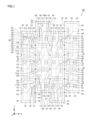
- FIG. 1 is a schematic plan view of the first surface side of the ceramic wiring member motherboard in the first embodiment.
- FIG. 2 is a schematic plan view of the second surface side of the ceramic wiring member motherboard in the first embodiment.
- FIG. 3 is a schematic plan view of the upper surface side of the ceramic wiring member.
- FIG. 4 is a schematic side view of the ceramic wiring member.
- FIG. 5 is a schematic cross-sectional view taken along line segment VV in FIGS. 3 and 6.
- FIG. 6 is a schematic plan view of the back side of the ceramic wiring member.
- FIG. 7 is a schematic side view of the ceramic wiring member.
- FIG. 8 is a schematic cross-sectional view taken along line segment VIII-VIII in FIGS. 3 and 6.
- FIG. 9 is a schematic plan view of the first surface side of the ceramic wiring member motherboard in the second embodiment.
- FIG. 10 is a schematic plan view of the second surface side of the ceramic wiring member motherboard in the second embodiment.
- the ceramic wiring member motherboard of the present disclosure has a first surface that is one surface in the thickness direction, and a second surface that is the surface opposite to the first surface in the thickness direction, and has a second surface that is one surface in the thickness direction.
- This is a ceramic wiring member motherboard in which a plurality of rectangular ceramic wiring members are laid out and connected together.
- the plurality of ceramic wiring members include a first ceramic wiring member and a second ceramic wiring member connected to the first ceramic wiring member.
- Each of the first ceramic wiring member and the second ceramic wiring member includes a ceramic main body portion having a plate-shaped portion, and a conductive portion disposed in contact with the main body portion.
- the conductive part includes a frame-shaped part disposed annularly on the main body along the outer periphery of the rectangle, and a pair arranged on a region of the main body surrounded by the frame-shaped part. an internal terminal, a pair of external terminals arranged on the main body apart from each other in a plan view on the second surface side, and a ground terminal arranged on the main body apart from the pair of external terminals. and, including.
- One of the pair of internal terminals and one of the pair of external terminals are electrically connected.
- the other of the pair of internal terminals and the other of the pair of external terminals are electrically connected.
- a break groove extending along each side of the rectangle of the plurality of adjacent ceramic wiring members is formed in at least one of the first surface and the second surface.
- the first ceramic wiring member and the second ceramic wiring member are arranged such that both ends of the first and second ceramic wiring members do not overlap with both ends of the second side.
- a first via hole that penetrates the ceramic wiring member motherboard in the thickness direction is formed in a region where the first side and the second side overlap.
- the conductive part is formed on the wall surrounding the first via hole, and connects the ground terminals of the first ceramic wiring member and the second ceramic wiring member to the frame-shaped parts of the first ceramic wiring member and the second ceramic wiring member.
- the first via conductor further includes a first via conductor.
- the first ceramic wiring member and the second ceramic wiring member are arranged point-symmetrically with respect to the first via conductor when viewed in the thickness direction of the ceramic wiring member motherboard.
- the plurality of ceramic wiring members are configured by using a first ceramic wiring member and a second ceramic wiring member that are connected to each other as a unit structure, and the unit structures are laid out without gaps.
- the first via hole is formed in a region where the first side of the first ceramic wiring member and the second side of the second ceramic wiring member overlap, and the first via hole
- the ground terminal and the frame portion are connected by a first via conductor formed on a wall surface surrounding the ground terminal.
- the first ceramic wiring is arranged along the first side and the second side.
- first ceramic wiring member and the second ceramic wiring member are point-symmetrical with respect to the first via conductor, with the first ceramic wiring member and the second ceramic wiring member being shifted from each other so that the first side and the second side partially overlap.
- first ceramic wiring member and the second ceramic wiring member after separation become ceramic wiring members having the same structure. As a result, efficiency of the manufacturing process is achieved.
- the ceramic wiring member motherboard of the present disclosure it is possible to improve the efficiency of the manufacturing process while maintaining the reliability of the electrical connection between the frame portion and the ground terminal.
- a first through hole penetrating from the first surface to the second surface may be formed at each rectangular vertex of the plurality of ceramic wiring members.
- the pair of internal terminals of the first ceramic wiring member and the pair of internal terminals of the second ceramic wiring member are located within the area surrounded by the frame-shaped portion. , they may be arranged in opposite directions in directions along the first side and the second side. With this configuration, even if the internal terminals are unevenly arranged due to the structure of the electronic component to be held in the ceramic wiring member, it is possible to improve the efficiency of the manufacturing process.
- the ceramic wiring member of the present disclosure includes a ceramic main body having a plate-like part and a conductive part disposed in contact with the main body, and has a rectangular shape when viewed in a direction perpendicular to the plate-like part.
- This is a ceramic wiring member having a shape.
- the plate-shaped portion has a first main surface that is one main surface in the thickness direction, and a second main surface located on the opposite side to the first main surface in the thickness direction.
- the conductive part includes a frame-shaped part arranged annularly on the main body part along the outer periphery of the rectangle, and a pair arranged on a region of the main body surrounded by the frame-shaped part, in a plan view on the first main surface side. and a pair of external terminals arranged on the main body apart from each other in a plan view on the second main surface side, and a ground terminal arranged on the main body apart from the pair of external terminals. and, including.
- the conductive portion further includes a first via conductor formed on the wall surface of the first groove portion and connecting the ground terminal and the frame portion.
- the outer periphery of the ceramic wiring member has a third side, which is a side of the rectangle in which the first groove is formed, spaced apart from the apex. and a second notch formed away from the apex on the fourth side opposite to the third side. The first notch portion and the second notch portion are located on the same straight line orthogonal to the third side and the fourth side.
- the ceramic wiring member of the present disclosure maintains the reliability of the electrical connection between the frame portion and the ground terminal by dividing the ceramic wiring member motherboard of the present disclosure into ceramic wiring members along the break groove. However, it can be manufactured efficiently.
- the first notch part and the second notch part are formed corresponding to a region where the break groove of the ceramic wiring member motherboard branches.
- the first notch portion and the second notch portion may penetrate the ceramic wiring member in the thickness direction of the main body portion.
- the first notch and the second notch are formed by forming a first through hole in the ceramic wiring member motherboard.
- the first notch portion and the second notch portion may be arranged biased to one side in the direction along the third side and the fourth side.
- FIG. 1 is a schematic plan view of a first surface side of a ceramic wiring member motherboard in Embodiment 1, which is an embodiment of the present disclosure.
- FIG. 2 is a schematic plan view of the second surface side of the ceramic wiring member motherboard in the first embodiment.
- FIG. 3 is a schematic plan view of the upper surface side of the ceramic wiring member.
- FIG. 4 is a schematic side view of the ceramic wiring member.
- FIG. 5 is a schematic cross-sectional view taken along line segment VV in FIGS. 3 and 6.
- FIG. FIG. 6 is a schematic plan view of the back side of the ceramic wiring member.
- FIG. 7 is a schematic side view of the ceramic wiring member.
- FIG. 8 is a schematic cross-sectional view taken along line segment VIII-VIII in FIGS. 3 and 6.
- ceramic wiring member motherboard 100 of the present embodiment has a first surface 100A (see FIG. 1), which is one surface in the thickness direction (Z-axis direction), and It has a second surface 100B (see FIG. 2) which is a surface opposite to the first surface 100A.
- the ceramic wiring member motherboard 100 has a structure in which a plurality of rectangular ceramic wiring members 110 and 120 are laid out and connected together when viewed in the thickness direction (viewed along the Z-axis direction). are doing.
- the plurality of ceramic wiring members 110 and 120 include a first ceramic wiring member 110 and a second ceramic wiring member 120 connected to the first ceramic wiring member 110.
- the first ceramic wiring member 110 and the second ceramic wiring member 120 are arranged in different directions within the ceramic wiring member motherboard 100, they have the same structure as described below based on FIGS. 3 to 8. This is a ceramic wiring member 1 having:
- ceramic wiring member 1 (first ceramic wiring member 110 and second ceramic wiring member 120, respectively) is arranged in contact with ceramic main body 10 and main body 10.
- a conductive part 20 is included.
- the ceramic constituting the main body portion 10 is not particularly limited, but for example, alumina (aluminum oxide) can be used.
- the main body portion 10 includes a plate-shaped portion 11 having a flat plate shape and a frame 12.
- the plate-shaped portion 11 has a rectangular shape when viewed in the thickness direction (Z-axis direction).
- the plate-shaped portion 11 includes a first main surface 11A and a second main surface 11B located on the opposite side in the thickness direction from the first main surface 11A.
- the thickness t of the main body portion 10 can be, for example, 0.1 mm or more and 0.6 mm or less.
- the frame body 12 has a frame-like shape rising from the outer edge of the first main surface 11A of the plate-shaped portion 11. More specifically, it has an annular shape along the outer edge of the first main surface 11A of the plate-like portion 11, which has a rectangular planar shape. When viewed in a direction perpendicular to the first main surface 11A, the frame 12 surrounds a cavity 50, which is a space above the first main surface 11A.
- the frame body 12 includes a planar first end surface 12A and a second end surface 12B that is a planar end surface on the opposite side of the first end surface 12A in the thickness direction of the plate-shaped portion 11.
- the frame body 12 is connected to the first main surface 11A of the plate-shaped portion 11 at the second end surface 12B.
- the first end surface 12A is located on a single plane over the entire area.
- the cavity 50 can be closed by placing the flat lid member on the first end surface 12A.
- the cavity 50 can house electronic components such as crystal elements that require airtightness.
- Such a ceramic wiring member 1 can be used as a ceramic package for accommodating electronic components. For example, when electrodes attached to both surfaces of a crystal element are respectively connected to a pair of internal terminals 22, a crystal resonator is constructed.
- the conductive part 20 includes a frame part 21, a pair of internal terminals 22, a pair of external terminals 23, a pair of ground terminals 24, a first via conductor 28, a second via conductor 25, and a third via conductor. 27, a first connecting portion 26, and a second connecting portion 29.
- the frame portion 21 is arranged to cover the first end surface 12A of the frame body 12.
- the frame portion 21 has an annular shape corresponding to the first end surface 12A of the frame body 12. That is, in a plan view on the first surface 100A side (viewpoint in FIGS. 1 and 3), the frame portion 21 extends along the outer periphery of the ceramic wiring member 1 having a rectangular shape. arranged in a ring at the top.
- the pair of internal terminals 22 are disposed in contact with and on the first main surface 11A of the plate-shaped portion 11 surrounded by the frame 12. That is, in a plan view on the first surface 100A side, the pair of internal terminals 22 are arranged on a region surrounded by the frame-shaped part 21 of the first main surface 11A of the plate-shaped part 11 included in the main body part 10. has been done.
- the frame 12 may be omitted. That is, the conductive part 20 includes a frame part 21, a pair of internal terminals 22, a pair of external terminals 23, a pair of ground terminals 24, a first via conductor 28, a second via conductor 25, and a third via conductor 28. It includes a via conductor 27, a first connection part 26, and a second connection part 29.
- the frame portion 21 extends along the outer periphery of the ceramic wiring member 1 having a rectangular shape. are arranged in an annular shape on the first main surface 11A of.
- the pair of internal terminals 22 are arranged in contact with each other on the first main surface 11A.
- the pair of internal terminals 22 are disposed on a region surrounded by the frame portion 21 of the first main surface 11A of the plate portion 11 included in the main body portion 10. There is.
- a bathtub-shaped lid member having a cavity on the frame portion 21, electronic components such as crystal elements that require airtightness can be stored in the cavity of the lid member.
- Such a ceramic wiring member 1 can be used as a ceramic package for accommodating electronic components. For example, when electrodes attached to both surfaces of a crystal element are respectively connected to a pair of internal terminals 22, a crystal resonator is constructed.
- the pair of external terminals 23 are arranged on the second main surface 11B of the plate-shaped portion 11 in contact with each other. That is, in a plan view on the second surface 100B side (viewpoint in FIGS. 2 and 6), the pair of external terminals 23 are spaced apart from each other on the second main surface 11B of the plate-shaped portion 11 included in the main body portion 10. It is located.
- the pair of ground terminals 24 are disposed apart from the pair of external terminals 23 and in contact with the second main surface 11B of the plate-shaped portion 11.
- the pair of ground terminals 24 are spaced apart from the pair of external terminals 23 and spaced apart from each other on the second main surface 11B of the plate-shaped portion 11 included in the main body portion 10. It is arranged as follows. In a plan view of the second surface 100B, the pair of external terminals 23 are arranged on one diagonal of the rectangle, and the pair of ground terminals 24 are arranged on the other diagonal of the rectangle. A pair of external terminals 23 and a pair of ground terminals 24 are arranged at each of the four corners of the rectangle. Such a terminal arrangement can facilitate the wiring design of the external board to which the ceramic wiring member 1 is to be attached.
- the second via conductor 25 is arranged to extend from the first main surface 11A to the second main surface 11B of the plate-shaped portion 11. More specifically, the second via conductor 25 is formed to fill a through hole formed in the plate portion 11. The second via conductor 25 is physically and electrically connected to one of the pair of external terminals 23 at the end of the plate portion 11 on the second main surface 11B side.
- the first connecting portion 26 is formed on the first main surface 11A of the plate-like portion 11. The first connecting portion 26 connects one of the pair of internal terminals 22 and the second via conductor 25 .
- the second via conductor 25 is physically and electrically connected to one of the pair of internal terminals 22 at the end of the plate portion 11 on the first main surface 11A side. That is, one of the pair of internal terminals 22 and one of the pair of external terminals 23 are electrically connected via the first connection portion 26 and the second via conductor 25.
- the third via conductor 27 is arranged to extend from the first main surface 11A to the second main surface 11B of the plate-shaped portion 11. More specifically, the third via conductor 27 is formed to fill a through hole formed in the plate portion 11.
- the third via conductor 27 is physically and electrically connected to the other of the pair of external terminals 23 at the end of the plate-shaped portion 11 on the second main surface 11B side.
- the third via conductor 27 is physically and electrically connected to the other of the pair of internal terminals 22 at the end of the plate portion 11 on the first main surface 11A side. That is, the other of the pair of internal terminals 22 and the other of the pair of external terminals 23 are electrically connected via the third via conductor 27.
- the second connecting portion 29 electrically connects the pair of ground terminals 24 inside the plate-like portion 11 .
- the second connecting portion 29 may be formed on the second main surface 11B of the plate-shaped portion 11. In this case, it is preferable that a portion of the second connection portion 29 in the longitudinal direction is covered with an insulator. Thereby, when the ground terminals 24 are soldered to the wiring on the external board, it is possible to prevent connection failures caused by the ground terminals 24 being connected to each other by solder. Further, the second connecting portion 29 may be omitted. In this case, the ground terminal 24 that is not connected to the first via conductor 28 does not have a ground function. As a result, only one ground terminal 24 functions as a ground.
- a break groove 151 extending along each rectangular side of a plurality of adjacent ceramic wiring members 110, 120 is formed in the first surface 100A and the second surface 100B.
- break grooves 151 are formed on both the first surface 100A and the second surface 100B, but one may be omitted.
- the ceramic wiring member motherboard 100 can be divided along the break grooves 151.
- the depth of the break groove 151 can be, for example, 0.025 mm or more and 0.200 mm or less.
- a dummy portion made of the same material may be provided around the ceramic wiring member motherboard 100. By providing the dummy portion, unintended damage to the ceramic wiring member motherboard 100 can be prevented.
- the first ceramic wiring member 110 has a side 111 as a first side which is one of the sides of the rectangle, a side 112 opposite to the side 111, a side 113 perpendicular to the sides 111 and 112, and a side 113 opposite to the side 113. side 114.
- Side 111 and side 112 correspond to long sides extending along the Y-axis direction.
- Side 113 and side 114 correspond to short sides extending along the X-axis direction.
- the second ceramic wiring member 120 has a side 121 as a second side that is one of the sides of the rectangle, a side 122 opposite to the side 121, a side 123 perpendicular to the sides 121 and 122, and a side 123 opposite to the side 123.
- Side 121 and side 122 correspond to long sides extending along the Y-axis direction.
- Side 123 and side 124 correspond to short sides extending along the X-axis direction.
- the side 111 as the first side of the first ceramic wiring member 110 and the side 121 as the second side of the second ceramic wiring member 120 partially overlap, and both ends 111A, 111B of the side 111 and the side 121
- the first ceramic wiring member 110 and the second ceramic wiring member 120 are arranged so as not to overlap with both ends 121A and 121B. More specifically, the side 111 and the side 121 are arranged so as to be shifted in the Y-axis direction so that a portion corresponding to approximately half of their respective lengths overlaps.
- the side 111 and the side 121 become the side 71 as the third side of the ceramic wiring member 1 (see FIGS. 3 and 6).
- the side 112 and the side 122 become the side 72 as the fourth side of the ceramic wiring member 1.
- Side 113 and side 123 become side 73 of ceramic wiring member 1 .
- Side 114 and side 124 become side 74 of ceramic wiring member 1 .
- a first via hole 131 that penetrates the ceramic wiring member motherboard 100 in the thickness direction is formed in a region where the side 111 as the first side and the side 121 as the second side overlap.
- the first via holes 131 become the first groove portions 31 of the ceramic wiring member 1 when the ceramic wiring member motherboard 100 is divided along the break grooves 151 (see FIGS. 3, 4, and 6).
- the first groove portion 31 is formed on the outer periphery of the main body portion 10 .
- the first groove portion 31 passes through the main body portion 10 in the thickness direction away from the apex of the rectangle.
- the first groove portion 31 passes through the frame portion 21 , the frame body 12 , the plate portion 11 , and one of the pair of ground terminals 24 .
- the first via conductor 28 is formed on the wall surrounding the first via hole 131.
- the first via conductor 28 fills the first via hole 131.
- the first via conductor 28 may cover the wall surface of the first via hole 131 without filling the first via hole 131.
- the first via conductor 28 connects one of the pair of ground terminals 24 of the first ceramic wiring member 110 and the second ceramic wiring member 120 and the frame portion 21 of the first ceramic wiring member 110 and the second ceramic wiring member 120. Physically and electrically connected.
- the first via conductor 28 of the ceramic wiring member motherboard 100 is formed on the wall surface defining the first groove portion 31. (See Figures 3, 4 and 6).
- the first via conductor 28 physically and electrically connects one of the pair of ground terminals 24 and the frame portion 21 .
- a first through hole 161 that penetrates from the first surface 100A to the second surface 100B is formed at each vertex of the rectangle of the plurality of ceramic wiring members 110, 120. .
- the first through hole 161 is formed on a straight line 191 extending in the X-axis direction so as to include the short sides 113 and 114 of the first ceramic wiring member 110 and on the X axis so as to include the short sides 123 and 124 of the second ceramic wiring member 120. It is arranged on a straight line 192 extending in the axial direction.
- the first through hole 161 has a first notch 41, a second notch 42, a third notch 43, and a fourth notch. 44, a fifth notch 45, and a sixth notch 46 (see FIGS. 3 and 6).
- the first notch 41 is formed on the third side 71 on which the first groove 31 is formed, away from the apex.
- the second notch portion 42 is formed on a side 72 as a fourth side opposite to the side 71, away from the apex.
- the third notch 43 is formed at a position corresponding to the intersection of the sides 71 and 74.
- the fourth notch 44 is formed at a position corresponding to the intersection of sides 71 and 73.
- the fifth notch 45 is formed at a position corresponding to the intersection of the sides 72 and 73.
- the sixth notch 46 is formed at a position corresponding to the intersection of the sides 72 and 74.
- the first notch 41 , the second notch 42 , the third notch 43 , the fourth notch 44 , the fifth notch 45 , and the sixth notch 46 It penetrates the portion 10 in the thickness direction.
- the first notch portion 41 and the second notch portion 42 are located on a straight line 91 that is orthogonal to the side 71 as the third side and the side 72 as the fourth side.
- the width w of the first notch 41 and the second notch 42 can be, for example, more than 0 ⁇ m and less than 40 ⁇ m.
- the depth d of the first notch 41 and the second notch 42 can be, for example, more than 0 ⁇ m and less than 50 ⁇ m.
- the first through hole 161 can be omitted.
- the first notch 41 and the second notch 42 are formed without penetrating the ceramic wiring member 1 in the thickness direction. (See Figures 3 and 6). More specifically, the first notch 41 and the second notch 42 are formed to have a depth corresponding to the depth of the break groove 151. This is because when forming the break grooves 151 in the manufacturing process, the break grooves 151 are intentionally formed so as to slightly intersect each other in the area where the break grooves 151 diverge, in order to avoid interruption in the area where the break grooves 151 diverge. It's for a reason.
- the break grooves 151 are separated by a distance corresponding to the desired size of the first notch part 41 and the second notch part 42. All you have to do is cross them. Note that when the break grooves 151 are formed in the green sheet by laser irradiation in the manufacturing process, the irradiated area evaporates. In the region where the break grooves 151 intersect, the laser is irradiated twice, so volatilization progresses more. Therefore, in the area where the break grooves 151 intersect, the depth of the break grooves 151 is, for example, more than 1 times and 1.2 times deeper than other parts.
- the first ceramic wiring member 110 and the second ceramic wiring member 120 which are the ceramic wiring members 1 having the same structure as described above, are arranged in the thickness direction of the ceramic wiring member motherboard 100. As seen in FIG. 2, they are arranged point-symmetrically with respect to the first via conductor 28 (so that they overlap entirely when rotated by 180 degrees around the first via conductor 28).
- the plurality of ceramic wiring members 110 and 120 included in the ceramic wiring member motherboard 100 have the first ceramic wiring member 110 and the second ceramic wiring member 120 connected to each other as a unit structure, and these unit structures are laid out without gaps. It is constructed according to the following.
- the first via hole 131 is formed in a region where the side 111 of the first ceramic wiring member 110 and the side 121 of the second ceramic wiring member 120 overlap, and A first via conductor 28 formed on a wall surrounding the via hole 131 connects the ground terminal 24 and the frame portion 21 .
- the first via hole 131 and the first via conductor 28 are arranged at positions corresponding to the sides of the rectangle.
- the first ceramic wiring member 110 and the second ceramic wiring member 120 are separated, the contact area between the first via conductor 28 and the wall surface of the first via hole 131 increases, and the first via conductor 28 is prevented from falling off. be done. Further, the first ceramic wiring member 110 and the second ceramic wiring member 120 are arranged point-symmetrically with respect to the first via conductor 28 in a state where they are shifted from each other so that the sides 111 and 121 partially overlap. As a result, the first ceramic wiring member 110 and the second ceramic wiring member 120 after separation become the ceramic wiring member 1 having the same structure. As a result, efficiency of the manufacturing process is achieved. Furthermore, even when an electronic component is mounted on the ceramic wiring member 1 and is sealed by the lid so that the electronic component cannot be seen, the first via hole 131 (the first groove 31 after separation) and the first via conductor 28 This makes it possible to grasp the orientation of electronic components.
- the ceramic wiring member motherboard 100 of the present embodiment can achieve efficiency in the manufacturing process while maintaining the reliability of the electrical connection between the frame portion 21 and the ground terminal 24.
- This is a ceramic wiring member motherboard.
- first via holes 131 penetrating from the first surface 100A to the second surface 100B are provided at each vertex of the rectangle of the plurality of ceramic wiring members 110, 120. is formed.
- the break grooves 151 extending in the X-axis direction and the break grooves 151 extending in the Y-axis direction can be positioned at desired positions. It is possible to connect.
- a pair of internal terminals 22 of the first ceramic wiring member 110 and a pair of internal terminals of the second ceramic wiring member 120 22 are arranged in opposite directions in the direction along the sides 111 and 121 (Y-axis direction) in the area surrounded by the frame-shaped part 21 .
- the ceramic wiring member 1 of the present embodiment is constructed by dividing the ceramic wiring member motherboard 100 of the present embodiment into the ceramic wiring members 1 along the break grooves 151. It has become possible to manufacture efficiently while maintaining the reliability of electrical connections.
- the first notch 41 and the second notch 42 penetrate the ceramic wiring member 1 in the thickness direction of the main body 10.
- the break grooves 151 extending perpendicularly to each other in the ceramic wiring member motherboard 100 can be connected to each other at desired positions, so that variations in the shape of the ceramic wiring member 1 can be suppressed.
- the first notch portion 41 and the second notch portion 42 are arranged biased to one side in the direction along the sides 111 and 121 (Y-axis direction). There is. As a result, even when an electronic component is mounted on the ceramic wiring member 1 and cannot be seen because it is sealed by the lid, the orientation of the electronic component can be adjusted by the first notch 41 and the second notch 42. It is now possible to understand.
- the ceramic wiring member motherboard 100 of the present embodiment described above can be manufactured, for example, by roughly the following procedure.
- a green sheet to become the main body 10 is prepared. Specifically, ceramic powder, such as alumina powder, constituting the main body 10, resin, solvent, etc. are mixed in a ball mill to obtain a slurry. This slurry is processed into a green sheet by a doctor blade method. As a result, a green sheet to become the main body portion 10 is obtained.
- a plurality of green sheets are prepared on the premise that the main body 10 will be constructed by stacking them.
- a paste to become the conductive part 20 is printed on the prepared green sheet.
- a paste is created by mixing and kneading additives, resin, solvent, etc. with powder of a conductor such as a metal.
- This paste is printed on a plurality of green sheets by, for example, screen printing.
- the first via holes 131 and the first through holes 161 are formed.
- the first via hole 131 is filled with the above paste.
- break grooves 151 are formed by, for example, laser irradiation. Thereafter, the ceramic wiring member motherboard 100 can be manufactured by firing the laminate.
- the ceramic wiring member 1 of the present embodiment described above can be manufactured by dividing the ceramic wiring member motherboard 100 along the break grooves 151.
- FIG. 9 is a schematic plan view of the first surface side of the ceramic wiring member motherboard in the second embodiment.
- FIG. 10 is a schematic plan view of the second surface side of the ceramic wiring member motherboard in the second embodiment.
- a ceramic wiring member motherboard 100 according to the second embodiment basically has the same configuration as the first embodiment, and has similar effects. It can be produced in the same way.
- the ceramic wiring member motherboard 100 of the second embodiment differs from that of the first embodiment in the positional relationship between the first ceramic wiring member 110 and the second ceramic wiring member 120.
- Embodiment 1 differences from Embodiment 1 will be explained.
- the first ceramic wiring member 110 and the second ceramic wiring member 120 constituting the unit structure have a side 111 as a first side of the first ceramic wiring member 110, and a side 111 as a first side of the first ceramic wiring member 110,
- the side 121 serving as the second side of the ceramic wiring member 120 is arranged so as to be shifted in the Y-axis direction so that a portion corresponding to 3/4 of the length of each side overlaps with the side 121 .
- the unit structures adjacent to each other in the short side direction (X-axis direction) of the rectangle are arranged so that the side 122 and the side 112 overlap at 3/4 of the total length.
- the ceramic wiring member 1 of the second embodiment has a change in the formation position of the first through hole 161 due to the difference in the positional relationship between the first ceramic wiring member 110 and the second ceramic wiring member 120.
- the structure is similar to that of the first embodiment, except that the formation positions of the first notch 41 and the second notch 42 change in the Y-axis direction, and the same effects are achieved.
Landscapes
- Engineering & Computer Science (AREA)
- Manufacturing & Machinery (AREA)
- Microelectronics & Electronic Packaging (AREA)
- Structure Of Printed Boards (AREA)
- Printing Elements For Providing Electric Connections Between Printed Circuits (AREA)
Priority Applications (3)
| Application Number | Priority Date | Filing Date | Title |
|---|---|---|---|
| JP2024537681A JP7833552B2 (ja) | 2022-07-29 | 2023-07-21 | セラミック配線部材母基板およびセラミック配線部材 |
| CN202380047285.1A CN119366270A (zh) | 2022-07-29 | 2023-07-21 | 陶瓷布线构件母基板以及陶瓷布线构件 |
| TW112128278A TWI871716B (zh) | 2022-07-29 | 2023-07-28 | 陶瓷配線構件母基板及陶瓷配線構件 |
Applications Claiming Priority (2)
| Application Number | Priority Date | Filing Date | Title |
|---|---|---|---|
| JPPCT/JP2022/029313 | 2022-07-29 | ||
| JP2022029313 | 2022-07-29 |
Publications (1)
| Publication Number | Publication Date |
|---|---|
| WO2024024683A1 true WO2024024683A1 (ja) | 2024-02-01 |
Family
ID=89706453
Family Applications (1)
| Application Number | Title | Priority Date | Filing Date |
|---|---|---|---|
| PCT/JP2023/026861 Ceased WO2024024683A1 (ja) | 2022-07-29 | 2023-07-21 | セラミック配線部材母基板およびセラミック配線部材 |
Country Status (4)
| Country | Link |
|---|---|
| JP (1) | JP7833552B2 (https=) |
| CN (1) | CN119366270A (https=) |
| TW (1) | TWI871716B (https=) |
| WO (1) | WO2024024683A1 (https=) |
Citations (4)
| Publication number | Priority date | Publication date | Assignee | Title |
|---|---|---|---|---|
| JP2000357604A (ja) * | 1999-06-17 | 2000-12-26 | Rohm Co Ltd | 集合基板 |
| JP2008302571A (ja) * | 2007-06-07 | 2008-12-18 | Denso Corp | セラミック基板の製造方法 |
| JP2013247449A (ja) * | 2012-05-24 | 2013-12-09 | Kyocera Corp | 圧電振動素子収納用パッケージおよび圧電装置ならびに多数個取り配線基板 |
| WO2019107298A1 (ja) * | 2017-11-29 | 2019-06-06 | Ngkエレクトロデバイス株式会社 | シート基板およびシート基板の製造方法 |
Family Cites Families (1)
| Publication number | Priority date | Publication date | Assignee | Title |
|---|---|---|---|---|
| JP3699609B2 (ja) * | 1999-04-28 | 2005-09-28 | 京セラ株式会社 | 電子部品搭載用基板 |
-
2023
- 2023-07-21 CN CN202380047285.1A patent/CN119366270A/zh active Pending
- 2023-07-21 JP JP2024537681A patent/JP7833552B2/ja active Active
- 2023-07-21 WO PCT/JP2023/026861 patent/WO2024024683A1/ja not_active Ceased
- 2023-07-28 TW TW112128278A patent/TWI871716B/zh active
Patent Citations (4)
| Publication number | Priority date | Publication date | Assignee | Title |
|---|---|---|---|---|
| JP2000357604A (ja) * | 1999-06-17 | 2000-12-26 | Rohm Co Ltd | 集合基板 |
| JP2008302571A (ja) * | 2007-06-07 | 2008-12-18 | Denso Corp | セラミック基板の製造方法 |
| JP2013247449A (ja) * | 2012-05-24 | 2013-12-09 | Kyocera Corp | 圧電振動素子収納用パッケージおよび圧電装置ならびに多数個取り配線基板 |
| WO2019107298A1 (ja) * | 2017-11-29 | 2019-06-06 | Ngkエレクトロデバイス株式会社 | シート基板およびシート基板の製造方法 |
Also Published As
| Publication number | Publication date |
|---|---|
| JP7833552B2 (ja) | 2026-03-19 |
| TW202423204A (zh) | 2024-06-01 |
| TWI871716B (zh) | 2025-02-01 |
| JPWO2024024683A1 (https=) | 2024-02-01 |
| CN119366270A (zh) | 2025-01-24 |
Similar Documents
| Publication | Publication Date | Title |
|---|---|---|
| KR101506256B1 (ko) | 칩 부품 구조체 및 제조방법 | |
| JP5668627B2 (ja) | 回路モジュール | |
| CN1093318C (zh) | 半导体装置及其制造方法 | |
| CN102986313B (zh) | 部件内置布线基板 | |
| CN100543977C (zh) | 电子部件搭载用封装及封装组合基板 | |
| US9781828B2 (en) | Module substrate and method for manufacturing module substrate | |
| JPH0837250A (ja) | 積層電子部品およびその製造方法 | |
| JP3918101B2 (ja) | 内部導体の接続構造及び多層基板 | |
| JP5799973B2 (ja) | セラミック多層配線基板およびこれを備えるモジュール | |
| JP2017076698A (ja) | 配線基板およびその製造方法 | |
| JP7833552B2 (ja) | セラミック配線部材母基板およびセラミック配線部材 | |
| JP5557924B2 (ja) | 多数個取り配線基板および配線基板ならびに電子装置 | |
| JP2005294697A (ja) | 電子部品及びその製造方法 | |
| JP3426988B2 (ja) | 多数個取り配線基板 | |
| JP7011563B2 (ja) | 回路基板および電子部品 | |
| JP4049134B2 (ja) | 電子部品の製造方法 | |
| JP7244294B2 (ja) | セラミックパッケージおよびその製造方法 | |
| US20250336575A1 (en) | Packaged electrical devices and related methods | |
| JP2014044979A (ja) | 配線基板 | |
| WO2011077968A1 (ja) | 回路モジュールの製造方法、回路モジュール及び回路モジュールを備える電子機器 | |
| JP7016426B2 (ja) | 基板の加工方法 | |
| JP2024145867A (ja) | アンテナ装置 | |
| JP2024143541A (ja) | セラミック配線部材 | |
| JP4276284B2 (ja) | 電子部品の製造方法および電子部品用母基板 | |
| JP4511573B2 (ja) | 電子部品およびこれを備えた電子機器 |
Legal Events
| Date | Code | Title | Description |
|---|---|---|---|
| 121 | Ep: the epo has been informed by wipo that ep was designated in this application |
Ref document number: 23846413 Country of ref document: EP Kind code of ref document: A1 |
|
| WWE | Wipo information: entry into national phase |
Ref document number: 2024537681 Country of ref document: JP |
|
| WWE | Wipo information: entry into national phase |
Ref document number: 202380047285.1 Country of ref document: CN |
|
| WWP | Wipo information: published in national office |
Ref document number: 202380047285.1 Country of ref document: CN |
|
| NENP | Non-entry into the national phase |
Ref country code: DE |
|
| 122 | Ep: pct application non-entry in european phase |
Ref document number: 23846413 Country of ref document: EP Kind code of ref document: A1 |