WO2023233565A1 - バンドギャップ電源回路 - Google Patents
バンドギャップ電源回路 Download PDFInfo
- Publication number
- WO2023233565A1 WO2023233565A1 PCT/JP2022/022244 JP2022022244W WO2023233565A1 WO 2023233565 A1 WO2023233565 A1 WO 2023233565A1 JP 2022022244 W JP2022022244 W JP 2022022244W WO 2023233565 A1 WO2023233565 A1 WO 2023233565A1
- Authority
- WO
- WIPO (PCT)
- Prior art keywords
- transistor
- power supply
- circuit
- terminal
- resistor
- Prior art date
- Legal status (The legal status is an assumption and is not a legal conclusion. Google has not performed a legal analysis and makes no representation as to the accuracy of the status listed.)
- Ceased
Links
Images




Classifications
-
- H—ELECTRICITY
- H02—GENERATION; CONVERSION OR DISTRIBUTION OF ELECTRIC POWER
- H02M—APPARATUS FOR CONVERSION BETWEEN AC AND AC, BETWEEN AC AND DC, OR BETWEEN DC AND DC, AND FOR USE WITH MAINS OR SIMILAR POWER SUPPLY SYSTEMS; CONVERSION OF DC OR AC INPUT POWER INTO SURGE OUTPUT POWER; CONTROL OR REGULATION THEREOF
- H02M1/00—Details of apparatus for conversion
- H02M1/36—Means for starting or stopping converters
-
- G—PHYSICS
- G05—CONTROLLING; REGULATING
- G05F—SYSTEMS FOR REGULATING ELECTRIC OR MAGNETIC VARIABLES
- G05F3/00—Non-retroactive systems for regulating electric variables by using an uncontrolled element, or an uncontrolled combination of elements, such element or such combination having self-regulating properties
- G05F3/02—Regulating voltage or current
- G05F3/08—Regulating voltage or current wherein the variable is DC
- G05F3/10—Regulating voltage or current wherein the variable is DC using uncontrolled devices with non-linear characteristics
- G05F3/16—Regulating voltage or current wherein the variable is DC using uncontrolled devices with non-linear characteristics being semiconductor devices
- G05F3/20—Regulating voltage or current wherein the variable is DC using uncontrolled devices with non-linear characteristics being semiconductor devices using diode- transistor combinations
- G05F3/24—Regulating voltage or current wherein the variable is DC using uncontrolled devices with non-linear characteristics being semiconductor devices using diode- transistor combinations wherein the transistors are of the field-effect type only
-
- G—PHYSICS
- G05—CONTROLLING; REGULATING
- G05F—SYSTEMS FOR REGULATING ELECTRIC OR MAGNETIC VARIABLES
- G05F3/00—Non-retroactive systems for regulating electric variables by using an uncontrolled element, or an uncontrolled combination of elements, such element or such combination having self-regulating properties
- G05F3/02—Regulating voltage or current
- G05F3/08—Regulating voltage or current wherein the variable is DC
- G05F3/10—Regulating voltage or current wherein the variable is DC using uncontrolled devices with non-linear characteristics
- G05F3/16—Regulating voltage or current wherein the variable is DC using uncontrolled devices with non-linear characteristics being semiconductor devices
- G05F3/20—Regulating voltage or current wherein the variable is DC using uncontrolled devices with non-linear characteristics being semiconductor devices using diode- transistor combinations
- G05F3/26—Current mirrors
-
- H—ELECTRICITY
- H02—GENERATION; CONVERSION OR DISTRIBUTION OF ELECTRIC POWER
- H02M—APPARATUS FOR CONVERSION BETWEEN AC AND AC, BETWEEN AC AND DC, OR BETWEEN DC AND DC, AND FOR USE WITH MAINS OR SIMILAR POWER SUPPLY SYSTEMS; CONVERSION OF DC OR AC INPUT POWER INTO SURGE OUTPUT POWER; CONTROL OR REGULATION THEREOF
- H02M3/00—Conversion of DC power input into DC power output
- H02M3/02—Conversion of DC power input into DC power output without intermediate conversion into AC
- H02M3/04—Conversion of DC power input into DC power output without intermediate conversion into AC by static converters
- H02M3/10—Conversion of DC power input into DC power output without intermediate conversion into AC by static converters using discharge tubes with control electrode or semiconductor devices with control electrode
- H02M3/145—Conversion of DC power input into DC power output without intermediate conversion into AC by static converters using discharge tubes with control electrode or semiconductor devices with control electrode using devices of a triode or transistor type requiring continuous application of a control signal
- H02M3/155—Conversion of DC power input into DC power output without intermediate conversion into AC by static converters using discharge tubes with control electrode or semiconductor devices with control electrode using devices of a triode or transistor type requiring continuous application of a control signal using semiconductor devices only
- H02M3/156—Conversion of DC power input into DC power output without intermediate conversion into AC by static converters using discharge tubes with control electrode or semiconductor devices with control electrode using devices of a triode or transistor type requiring continuous application of a control signal using semiconductor devices only with automatic control of output voltage or current, e.g. switching regulators
- H02M3/158—Conversion of DC power input into DC power output without intermediate conversion into AC by static converters using discharge tubes with control electrode or semiconductor devices with control electrode using devices of a triode or transistor type requiring continuous application of a control signal using semiconductor devices only with automatic control of output voltage or current, e.g. switching regulators including plural semiconductor devices as final control devices for a single load
Definitions
- the present disclosure relates to a bandgap power supply circuit.
- a bandgap power supply circuit is a circuit widely used in various LSIs (Large Scale Integration), and is composed of a bandgap core circuit that generates a reference voltage and a startup circuit that starts up the bandgap core circuit. .
- LSIs Large Scale Integration
- various proposals have been made toward lowering the reference voltage generated by a bandgap power supply circuit.
- Non-Patent Document 1 describes a bandgap power supply circuit in which the output voltage of the bandgap core circuit is about 1.2V.
- the bandgap core circuit includes an operational amplifier OP1, which is a differential amplifier circuit, a diode D1, a diode D2, a transistor MP1, a transistor MP2, a transistor MP3, a resistor R1, a resistor R2, a resistor R3, and a resistor R4.
- the gate terminals of the transistors MP1 to MP3 are connected to the output terminal of the operational amplifier OP1.
- An anode terminal of a diode D1 in a parallel circuit of a diode D1 and a resistor R1 is connected to the positive input terminal of the operational amplifier OP1, and a cathode terminal of the diode D1 in the parallel circuit is set to the ground potential VSS.
- the drain terminal of transistor MP1 is connected to the positive input terminal of operational amplifier OP1 and the anode terminal of diode D1.
- the anode terminal of a diode D2 is connected to the negative input terminal of the operational amplifier OP1 via a resistor R3, and the resistor R2 is connected in parallel to a current path in which the diode D2 and the resistor R3 are connected in series.
- the cathode terminal of the diode D2 and one terminal of the resistor R2 are set to the ground potential VSS.
- the drain terminal of the transistor MP2 is connected to the negative input terminal of the operational amplifier OP1 and the resistor R3 of the current path. Note that the junction area of the diode D1 is smaller than the junction area of the diode D2.
- One terminal of the resistor R4 and the drain terminal of the transistor MP3 are connected to the output terminal of the bandgap core circuit.
- the other terminal of the resistor R4 is set to the ground potential VSS.
- a power supply voltage VDD is supplied to each source terminal of the transistors MP1 to MP3.
- the operational amplifier OP1 is designed so that the sum of the forward voltage of the diode D2 with a large junction area and the voltage drop value of the resistor R3 connected in series with the diode D2 is equal to the forward voltage of the diode D1 with a small junction area. Controls the current flowing through D1 and diode D2. When the startup circuit activates the bandgap core circuit, current flows through the bandgap core circuit.
- the normal operating state is a state in which current flows from the anode terminal side to the cathode terminal side of both diode D1 and diode D2 (on state), and current also flows to resistor R1 and resistor R2.
- both the diode D1 and the diode D2 are in the OFF state during the process from starting the power supply that supplies the power supply voltage to the normal operating state, but the resistance There is a problem that current flows through R1 and resistor R2, which causes an abnormal operating state.
- the present disclosure is intended to solve the above problems, and aims to provide a bandgap power supply circuit that can transition to a normal operating state without going through an abnormal operating state.
- a bandgap power supply circuit includes a first current path in which a first resistor is connected in series, a first switch that turns on/off continuity between the first resistor and a ground potential, and a first switch that is parallel to the first current path.
- a first rectifying element connected to the ground potential and a second resistor constitute a second current path connected in series, and a second switch for turning on/off continuity between the second resistor and the ground potential and a third resistor are connected in series.
- a connected current path is configured, and the current path has a second rectifying element connected in parallel with the second current path, and the sum of the current flowing through the first rectifying element and the current flowing through the first current path.
- the device includes a bandgap core circuit that controls the forward voltage to be equal to the forward voltage, and a switch control circuit that controls the first switch and the second switch from off to on when a power supply that supplies power supply voltage is activated.
- the bandgap core circuit is configured such that the sum of the current flowing through the first rectifying element and the current flowing through the first current path, and the sum of the current flowing through the second rectifying element and the current flowing through the second current path. and the sum of the forward voltage of the second rectifying element and the voltage drop value at the third resistor is controlled to be equal to the forward voltage of the first rectifying element.
- the switch control circuit controls the first switch and the second switch from off to on when the power supply is started. Thereby, the bandgap power supply circuit according to the present disclosure can transition to a normal operating state without going through an abnormal operating state.
- FIG. 2 is a circuit diagram showing the configuration of a conventional example (1) of a bandgap core circuit.
- FIG. 2 is a circuit diagram showing the configuration of a conventional example (2) of a bandgap core circuit.
- 2 is a graph showing time waveforms of a voltage applied to a positive input terminal, a voltage applied to a negative input terminal, and a power supply voltage of an operational amplifier included in a conventional bandgap core circuit.
- 1 is a circuit diagram showing the configuration of a bandgap power supply circuit according to Embodiment 1.
- FIG. FIG. 2 is a circuit diagram showing the configuration of a bandgap power supply circuit according to a second embodiment.
- FIG. 3 is a circuit diagram showing the configuration of a bandgap power supply circuit according to a third embodiment.
- FIG. 1 is a circuit diagram showing the configuration of a bandgap core circuit 100, which is a conventional example (1).
- the bandgap core circuit 100 is a conventional circuit that is activated by a startup circuit and outputs a reference voltage V ref of about 1.2V.
- the bandgap core circuit 100 includes an operational amplifier OP1, a resistor R1, a resistor R3, a diode D1, a diode D2, a diode D3, a transistor MP1, a transistor MP2, and a transistor MP3.
- the diode D1 and the diode D3 have the same device structure, and the ratio of the junction area between the diode D1 and the diode D2 is 1:N.
- N is an integer greater than 1.
- Transistor MP1, transistor MP2, and transistor MP3 have the same device structure, and are, for example, P-channel transistors. Transistor MP1, transistor MP2, and transistor MP3 are connected in parallel to form a current mirror circuit.
- Each gate terminal of a transistor MP1, a transistor MP2, and a transistor MP3 is connected to the output terminal of the operational amplifier OP1.
- the anode terminal of the diode D1 and the drain terminal of the transistor MP1 are connected to the positive input terminal of the operational amplifier OP1.
- the cathode terminal of the diode D1 is set to the ground potential VSS.
- a voltage V1 is applied to the positive input terminal of the operational amplifier OP1, and a current I1 flows through the diode D1.
- the voltage across the terminals of diode D1 is V f1 .
- the negative input terminal of the operational amplifier OP1 is connected to the drain terminal of the transistor MP2, and is further connected to the anode terminal of the diode D2 via a resistor R3.
- the cathode terminal of the diode D2 is set to the ground potential VSS.
- a voltage V2 is applied to the negative input terminal of the operational amplifier OP1, and a current I2 flows through a current path in which a resistor R3 and a diode D2 are connected in series.
- the voltage across the diode D2 is V f2 and the voltage across the resistor R3 is dV f .
- the voltage dV f is the value of the voltage drop across resistor R3.
- a power supply voltage VDD is supplied to each source terminal of the transistor MP1, transistor MP2, and transistor MP3.
- An output terminal of the bandgap core circuit 100 is connected to one terminal of a resistor R1 and a drain terminal of a transistor MP3. Further, the other terminal of the resistor R1 is connected to the anode terminal of the diode D3, and the cathode terminal is set to the ground potential VSS.
- a current I3 flows through the resistor R1.
- the inter-terminal voltage V f1 of the diode D1, the inter-terminal voltage V f2 of the diode D2, and the inter-terminal voltage dV f of the resistor R3 are expressed by the following formula (1), the following formula (2), and the following formula (3).
- VT is the thermal voltage
- Is is the reverse saturation current per unit area
- A is the junction area of the diode D1.
- V f1 V T ⁇ ln ⁇ I 1 /(I S ⁇ A) ⁇ ...(1)
- V f2 V T ⁇ ln ⁇ I 2 /(I S ⁇ N ⁇ A) ⁇ ...(2)
- the reference voltage V ref generated by the bandgap core circuit 100 can be expressed by the following equation (4) according to the above equation (1), the above equation (2), and the above equation (3). Since the first term in equation (4) below has a negative temperature coefficient and the second term has a positive temperature coefficient, the temperature coefficients can be canceled out by appropriately adjusting each parameter.
- the bandgap core circuit 100 shown in FIG. 1 generates a reference voltage V ref of about 1.2V and outputs the reference voltage V ref from an output terminal.
- V ref V f1 + (R1/R3) ⁇ V T ⁇ ln(N) ... (4)
- FIG. 2 is a circuit diagram showing the configuration of a bandgap core circuit 101 which is a conventional example (2).
- the bandgap core circuit 101 is a bandgap core circuit included in the bandgap power supply circuit described in Non-Patent Document 1.
- the bandgap core circuit 101 is activated by a startup circuit and outputs a reference voltage V ref of about 1.2V.
- the bandgap core circuit 101 includes an operational amplifier OP1, a resistor R1, a resistor R2, a resistor R3, a resistor R4, a diode D1, a diode D2, a transistor MP1, a transistor MP2, and a transistor MP3.
- the diode D1 and the diode D2 have the same device structure, and the ratio of the junction area between the diode D1 and the diode D2 is 1:N.
- N is an integer greater than 1.
- Transistor MP1, transistor MP2, and transistor MP3 have the same device structure, and are, for example, P-channel transistors. Transistor MP1, transistor MP2, and transistor MP3 are connected in parallel to form a current mirror circuit.
- Each gate terminal of a transistor MP1, a transistor MP2, and a transistor MP3 is connected to the output terminal of the operational amplifier OP1.
- One terminal of a resistor R1, an anode terminal of a diode D1, and a drain terminal of a transistor MP1 are connected to the positive input terminal of the operational amplifier OP1.
- the other terminal of the resistor R1 and the cathode terminal of the diode D1 are set to the ground potential VSS.
- the negative input terminal of the operational amplifier OP1 is connected to the drain terminal of the transistor MP2, and further connected to the anode terminal of the diode D2 via a resistor R3.
- the cathode terminal of the diode D2 is set to the ground potential VSS.
- the resistor R2 is connected to the negative input terminal of the operational amplifier OP1 in parallel with a current path in which the resistor R3 and the diode D2 are connected in series. That is, one terminal of the resistor R2 is connected to the current path and the negative input terminal of the operational amplifier OP1, and the other terminal is connected to the ground potential VSS.
- a power supply voltage VDD is supplied to each source terminal of the transistor MP1, transistor MP2, and transistor MP3.
- An output terminal of the bandgap core circuit 101 is connected to one terminal of a resistor R4 and a drain terminal of a transistor MP3. Furthermore, the other terminal of the resistor R4 is set to the ground potential VSS. A current I3 flows through the resistor R4.
- the series circuit of resistor R1 and diode D3 in bandgap core circuit 100 is replaced with resistor R4 in bandgap core circuit 101.
- the bandgap core circuit 101 includes a resistor R1 connected in parallel to the diode D1, and a resistor R2 connected in parallel to a current path in which a resistor R3 and a diode D2 are connected in series.
- a current I 2a flowing through the current path between the resistor R3 and the diode D2 is expressed by the following equation (5)
- a current I 2b flowing through the resistor R2 is expressed by the following equation (6).
- I 2a dV f /R3
- I 2b V f1 /R2 (6)
- the conventional bandgap core circuit 100 has the following two stable states (1) and (2).
- (1) A state in which no current flows through the bandgap core circuit 100.
- (2) A state in which both diode D1 and diode D2 are in an on state, and current flows through diode D1, diode D2, resistor R1, and resistor R3, respectively.
- state (2) is a normal operating state.
- a start-up circuit is used to avoid condition (1). That is, the startup circuit activates the bandgap core circuit 100, thereby avoiding the condition (1).
- the following three stable states (1), (2), and (3) exist depending on variations in the resistance R1 or the resistance R2.
- (1) A state in which no current flows through the bandgap core circuit 101.
- (2) A state in which diode D1 and diode D2 are both off, and current flows through resistor R1 and resistor R2, respectively.
- (3) A state in which both diode D1 and diode D2 are on, and current flows through diode D1, diode D2, resistor R1, and resistor R2, respectively.
- the state (2) is the abnormal operating state
- the state (3) is the normal operating state.
- a start-up circuit is used to avoid condition (1). That is, the startup circuit activates the bandgap core circuit 101, thereby avoiding the condition (1).
- the startup circuit cannot prevent the occurrence of condition (2). Therefore, when the bandgap core circuit 101 is activated by the startup circuit, it transits through state (2) and then transitions to state (3). In this case, the bandgap core circuit 101 may be in the state (2) before the power supply voltage supplied from the power supply completes rising.
- FIG. 3 is a graph showing the time waveforms of the voltage V1 applied to the positive input terminal of the operational amplifier OP1 included in the bandgap core circuit 101, the voltage V2 applied to the negative input terminal, and the power supply voltage VDD.
- the time waveform A of the power supply voltage VDD starts to rise after the power supply is activated by the startup circuit, and after a certain period of time, the rise is completed and becomes a stable power supply voltage VDD.
- Voltage B is the threshold voltage of diodes D1 and D2.
- the voltage V1 applied to the positive input terminal of the operational amplifier OP1 is also the voltage applied to the anode terminal of the diode D1.
- the voltage V2 applied to the negative input terminal of the operational amplifier OP1 is also the voltage applied to the current path in which the resistor R3 and the diode D2 are connected in series.
- a waveform C of voltage V1 or V2 shows a waveform when the bandgap core circuit 101 has converged to a normal operating state. If the voltage V1 at the anode terminal of the diode D1 becomes equal to or higher than the voltage B before the rise of the power supply voltage VDD is completed, that is, before it converges to a constant power supply voltage VDD, the bandgap core circuit 101 is in a normal operating state. Become.
- a waveform D of voltage V1 or V2 shows a waveform when the bandgap core circuit 101 has converged to an abnormal operating state.
- voltage V1 at the anode terminal of diode D1 does not exceed voltage B before the rise of power supply voltage VDD is completed.
- a current flows through the resistor R1 and the resistor R2 before the power supply voltage VDD rises, and as shown in FIG. It takes time to converge to a normal operating state.
- the bandgap power supply circuit according to the first embodiment during the start-up process of the bandgap power supply circuit, that is, at the time of starting the power supply, no current flows through the resistor R1 and the resistor R2, and after the rise of the power supply voltage VDD is completed, the resistor Control is performed so that current flows through R1 and resistor R2.
- the bandgap power supply circuit according to the first embodiment can transit to state (3), which is a normal operating state, without passing through state (2), which is an abnormal operating state.
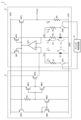
- FIG. 4 is a circuit diagram showing the configuration of the bandgap power supply circuit 1 according to the first embodiment.
- a bandgap power supply circuit 1 is a circuit that generates a reference voltage V ref based on a power supply voltage VDD, and includes a bandgap core circuit 2, a startup circuit 3, and a switch control circuit 4.
- the bandgap core circuit 2 includes an operational amplifier OP1, a transistor MP1, a transistor MP2, a transistor MP3, a diode D1, a diode D2, a resistor R1, a resistor R2, a resistor R3, a resistor R4, a switch SW1, and a switch SW2.
- the switch SW1 is a first switch in which a resistor R1, which is a first resistor, is connected in series to form a first current path, and turns on/off the conduction between the resistor R1 and the ground potential VSS.
- the first current path is a series circuit in which a resistor R1 and a switch SW1 are connected in series.
- One end of the resistor R1 is connected to the positive input terminal (+) of the operational amplifier OP1, and the other end is connected to the switch SW1.
- the switch SW2 is a second switch in which a resistor R2, which is a second resistor, is connected in series to form a second current path, and turns on/off the conduction between the resistor R2 and the ground potential VSS.
- the second current path is a series circuit in which a resistor R2 and a switch SW2 are connected in series.
- One end of the resistor R2 is connected to the negative input terminal (-) of the operational amplifier OP1, and the other end is connected to the switch SW2.
- the diode D1 is a first rectifying element connected in parallel with the first current path.
- the diode D1 is a first diode whose cathode terminal is connected to the ground GND and set to the ground potential VSS, and whose anode terminal is connected to one end of the resistor R1 and the positive input terminal of the operational amplifier OP1.
- the diode D2 is a second rectifying element that constitutes a current path in which a resistor R3, which is a third resistance, is connected in series, and the current path is connected in parallel with the second current path.
- One end of the resistor R3 is connected to the negative input terminal of the operational amplifier OP and one end of the resistor R2.
- the diode D2 is a second diode whose anode terminal is connected to the other end of the resistor R3 and whose cathode terminal is electrically connected to the ground GND to be at the ground potential VSS.
- the transistor MP1, the transistor MP2, and the transistor MP3 are a first transistor, a second transistor, and a third transistor having the same device structure, and for example, a P-channel transistor is used.
- Transistor MP1, transistor MP2, and transistor MP3 have their source terminals and drain terminals electrically connected by a control voltage applied to their gate terminals. Further, transistor MP1, transistor MP2, and transistor MP3 are connected in parallel to form a current mirror circuit.
- the diode D1 and the diode D2 have the same device structure, and the ratio of the junction areas between the diode D1 and the diode D2 is 1:N.
- N is an integer greater than 1.
- the diode D1 which has a small junction area, has a cathode terminal set to the ground potential VSS, and an anode terminal connected to the drain terminal of the transistor MP1.
- the source terminal of the transistor MP1 is connected to a power supply (not shown), and is supplied with a power supply voltage VDD from the power supply.
- the diode D2, which has a large junction area has a cathode terminal set to the ground potential VSS, and an anode terminal connected to the drain terminal of the transistor MP2 via a resistor R3.
- the source terminal of the transistor MP2 is connected to the power supply mentioned above, and is supplied with the power supply voltage VDD from the power supply.
- the operational amplifier OP1 is configured such that the sum of the forward voltage V f2 of the diode D2 and the voltage drop value dV f of the resistor R3 connected in series with the diode D2 is equal to the forward voltage V f1 of the diode D1.
- a differential amplifier circuit that controls the current flowing through the diode D1 and the diode D2.
- the resistor R4 has one end connected to the ground GND and set to the ground potential VSS, and the other end connected to the drain terminal of the transistor MP3 and the output terminal of the bandgap core circuit 2. That is, the bandgap power supply circuit 1 outputs the reference voltage V ref from the connection point between the transistor MP3 and the resistor R4.
- the startup circuit 3 is a circuit for activating the bandgap core circuit 2 and preventing the bandgap core circuit 2 from entering the state (1) in which no current flows.
- the startup circuit 3 includes a resistor R5, a transistor MP4, a transistor MP5, a transistor MP6, a transistor MN1, a transistor MN2, and a transistor MN3.
- transistor MP4, transistor MP5, and transistor MP6 are P-channel transistors.
- Transistor MN1, transistor MN2, and transistor MN3 are N-channel transistors.
- the gate terminal of the transistor MP4 is connected to each gate terminal of the transistor MP1, the transistor MP2, and the transistor MP3, and the source terminal is connected to the above power supply and is supplied with the power supply voltage VDD.
- the drain terminal of transistor MP4 is connected to the drain terminal of transistor MN1.
- the gate terminal of the transistor MN1 is connected to the gate terminal of the transistor MN2, and the source terminal is connected to the ground GND, so that the transistor MN1 has a ground potential VSS.
- Transistor MP4 and transistor MN1 constitute a bias circuit.
- the resistor R5 has one end connected to the power supply and supplied with the power supply voltage VDD, and the other end connected to the drain terminal of the transistor MN2.
- the source terminal of the transistor MN2 is connected to the ground GND and set to the ground potential VSS.
- Resistor R5 and transistor MN2 constitute a current-voltage conversion circuit.
- the gate terminal of the transistor MP5 is connected to the gate terminal of the transistor MN3, the source terminal is connected to the power supply and supplied with the power supply voltage VDD, and the drain terminal is connected to the drain terminal of the transistor MN3.
- the source terminal of the transistor MN3 is connected to the ground GND and set to the ground potential VSS.
- the gate terminal of the transistor MP5 and the gate terminal of the transistor MN3 are connected to a connection point between the resistor R5 and the drain terminal of the transistor MN2.
- the drain terminal of the transistor MP5 and the drain terminal of the transistor MN3 are connected to the gate terminal of the transistor MP6.
- Transistor MP5 and transistor MN3 constitute an inverter.
- the inverter receives the voltage at the drain terminal of the transistor MN2 (drain voltage), and has an output point at the connection point between the drain terminal of the transistor MP5 and the drain terminal of the transistor MN3.
- the transistor MP6 has a source terminal connected to the power supply and supplied with the power supply voltage VDD, and a drain terminal connected to the anode terminal of the diode D2 of the bandgap core circuit 2.
- the inverter and transistor MP6 constitute a starting bias circuit.
- the switch control circuit 4 controls the switch SW1 and the switch SW2 from off to on when the power supply is started. For example, when the startup circuit 3 starts the bandgap core circuit 2, the power supply is started and the rise of the power supply voltage VDD is started. The switch control circuit 4 turns off both the switch SW1 and the switch SW2 before the rise of the power supply voltage VDD is completed and the power supply voltage VDD converges to a constant voltage.
- switch control circuit 4 turns on both switch SW1 and switch SW2.
- the waveforms of voltages V1 and V2 converge to a voltage exceeding threshold voltage B. That is, the bandgap power supply circuit 1 can be brought into the state (3) without passing through the state (2) at the time of startup of the power supply, that is, before the rise of the power supply voltage VDD is completed.
- the configuration of the startup circuit 3 shown in FIG. 4 is an example, and a circuit different from the configuration shown in FIG. 4 may be used as long as it can start up the bandgap core circuit 2.
- a configuration is shown in which the operational amplifier OP1 is used in the bandgap core circuit 2
- a self-biased current mirror circuit may be used instead of the operational amplifier OP1.
- the current mirror circuit may use a transistor MN4a and a transistor MN5a (not shown in FIG. 4) in addition to the transistor MP1 and the transistor MP2.
- the gate terminals of transistor MP1 and transistor MP2, which are P-channel transistors, are connected to the gate terminals of transistor MP3 and transistor MP4 shown in FIG. Supplied.
- the drain terminal of transistor MP1 is connected to the drain terminal of transistor MN4a, which is an N-channel transistor
- the drain terminal of transistor MP2 is connected to the drain terminal of transistor MN5a, which is N-channel transistor.
- the gate terminal of transistor MN4a and the gate terminal of transistor MN5a are connected.
- the source terminal of the transistor MN4a corresponds to the positive input terminal of the operational amplifier OP1, and is connected to the parallel circuit of the first current path and the diode D1.
- the source terminal of the transistor MN5a corresponds to the negative input terminal of the operational amplifier OP1, and is connected to a parallel circuit of the second current path and a current path composed of the resistor R3 and the diode D1. Even with the bandgap power supply circuit 1 configured in this manner, it is possible to transition to a normal operating state without passing through an abnormal operating state.
- the diode D1 and the diode D2 may be PNP type bipolar transistors.
- the bandgap power supply circuit 1 As described above, in the bandgap power supply circuit 1 according to the first embodiment, the sum of the current I 1a flowing through the diode D1 and the current I 1b flowing through the first current path, the current I 2a flowing through the diode D2, and the second current A band that is controlled so that the sum of the currents I 2b flowing in the diode D2 and the sum of the forward voltage V f2 of the diode D2 and the voltage drop value dV f in the resistor R3 is equal to the forward voltage V f1 of the diode D1.
- the device includes a gap core circuit 2 and a switch control circuit 4 that controls the switch SW1 and the switch SW2 from off to on when the power supply is started. Thereby, the bandgap power supply circuit 1 can transition to a normal operating state without going through an abnormal operating state.
- the bandgap core circuit 2 includes an operational amplifier OP1 and transistors MP1, MP2, and MP3 whose respective gate terminals are connected to the output terminal of the operational amplifier OP1.
- the diode D1 has an anode terminal connected to the positive input terminal of the operational amplifier OP1 and a drain terminal of the transistor MP1, and a cathode terminal set to the ground potential VSS.
- the first current path is connected in parallel with the diode D1 between the positive input terminal of the operational amplifier OP1 and the ground potential VSS, and the second current path is provided between the negative input terminal of the operational amplifier OP1 and the ground potential VSS.
- the diode D2 has an anode terminal connected to the negative input terminal of the operational amplifier OP1 and a drain terminal of the transistor MP2 via a resistor R3, and a cathode terminal set to the ground potential VSS.
- the operational amplifier OP1 is configured such that the sum of the current I 1a flowing through the diode D1 and the current I 1b flowing through the first current path is equal to the sum of the current I 2a flowing through the diode D2 and the current I 2b flowing through the second current path, and the diode D2
- the sum of the forward voltage V f2 of the diode D1 and the voltage drop value dV f at the resistor R3 is controlled to be equal to the forward voltage V f1 of the diode D1.
- the switch control circuit 4 turns off both switch SW1 and switch SW2 before the rise of the power supply voltage VDD is completed at the time of starting the power supply, and the rise of the power supply voltage VDD is completed at the time of starting the power supply. After that, both switch SW1 and switch SW2 are turned on. Thereby, the bandgap power supply circuit 1 can transition to a normal operating state without going through an abnormal operating state.
- FIG. 5 is a circuit diagram showing the configuration of a bandgap power supply circuit 1A according to the second embodiment.
- a bandgap power supply circuit 1A includes a bandgap core circuit 2A, a startup circuit 3A, and a low pass filter 5 (hereinafter referred to as LPF 5).
- the bandgap core circuit 2A includes an operational amplifier OP1, a transistor MP1, a transistor MP2, a transistor MP3, a diode D1, a diode D2, a resistor R1, a resistor R2, a resistor R3, a resistor R4, a transistor MN4, and a transistor MN5.
- the transistor MN4 which is an N-channel transistor, has a drain terminal connected in series with a resistor R1 to form a first current path, and is a first switch that turns on and off conduction between the resistor R1 and the ground potential VSS.
- the first current path is a series circuit in which a resistor R1 and a transistor MN4 are connected in series.
- One end of the resistor R1 is connected to the positive input terminal (+) of the operational amplifier OP1, and the other end is connected to the transistor MN4.
- the transistor MN5 which is an N-channel transistor, has a drain terminal connected in series with a resistor R2 to form a second current path, and is a second switch that turns on and off conduction between the resistor R2 and the ground potential VSS.
- the second current path is a series circuit in which a resistor R2 and a transistor MN5 are connected in series.
- One end of the resistor R2 is connected to the negative input terminal (-) of the operational amplifier OP1, and the other end is connected to the transistor MN5.
- the diode D1 is a first rectifying element connected in parallel with the first current path.
- the diode D1 is a first diode whose cathode terminal is connected to the ground GND and set to the ground potential VSS, and whose anode terminal is connected to one end of the resistor R1 and the positive input terminal of the operational amplifier OP1.
- the diode D2 is a second rectifying element that constitutes a current path in which the resistor R3 is connected in series, and the current path is connected in parallel with the second current path.
- One end of the resistor R3 is connected to the negative input terminal of the operational amplifier OP and one end of the resistor R2.
- the diode D2 is a second diode whose anode terminal is connected to the other end of the resistor R3 and whose cathode terminal is electrically connected to the ground GND to be at the ground potential VSS.
- the transistor MP1, the transistor MP2, and the transistor MP3 are a first transistor, a second transistor, and a third transistor having the same device structure, and for example, a P-channel transistor is used.
- Transistor MP1, transistor MP2, and transistor MP3 have their source terminals and drain terminals electrically connected by a control voltage applied to their gate terminals. Further, transistor MP1, transistor MP2, and transistor MP3 are connected in parallel to form a current mirror circuit.
- the diode D1 and the diode D2 have the same device structure, and the ratio of the junction areas between the diode D1 and the diode D2 is 1:N.
- N is an integer greater than 1.
- the diode D1 which has a small junction area, has a cathode terminal set to the ground potential VSS, and an anode terminal connected to the drain terminal of the transistor MP1.
- the source terminal of the transistor MP1 is connected to a power supply (not shown), and is supplied with a power supply voltage VDD from the power supply.
- the diode D2, which has a large junction area has a cathode terminal set to the ground potential VSS, and an anode terminal connected to the drain terminal of the transistor MP2 via a resistor R3.
- the source terminal of the transistor MP2 is connected to the power supply mentioned above, and is supplied with the power supply voltage VDD from the power supply.
- the operational amplifier OP1 connects the diode D1 so that the sum of the forward voltage V f2 of the diode D2 and the voltage drop value dV f of the resistor R3 to which the diode D2 is connected in series is equal to the forward voltage V f1 of the diode D1. and a differential amplifier circuit that controls the current flowing through the diode D2.
- the resistor R4 has one end connected to the ground GND and set to the ground potential VSS, and the other end connected to the drain terminal of the transistor MP3 and the output terminal of the bandgap core circuit 2. That is, the bandgap power supply circuit 1A outputs the reference voltage V ref from the connection point between the transistor MP3 and the resistor R4.
- the startup circuit 3A is a circuit for starting the bandgap core circuit 2A and preventing the state (1) above in which no current flows through the bandgap core circuit 2A.
- the startup circuit 3A includes a resistor R5, a transistor MP4, a transistor MP5, a transistor MP6, a transistor MN1, a transistor MN2, and a transistor MN3. That is, the startup circuit 3A is configured similarly to the startup circuit 3 and functions similarly.
- the LPF5 is a switch control circuit that receives the power supply voltage VDD and uses an output signal to control on/off the transistors MN4 and MN5, and is a series circuit in which a resistor R6 and a capacitor C1 are connected in series.
- the resistor R6 has one end connected to the power supply and supplied with the power supply voltage VDD, and the other end connected to the capacitor C1.
- One end of the capacitor C1 is connected to the resistor R6, and the other end is connected to the ground GND to be at the ground potential VSS.
- the connection point between the resistor R6 and the capacitor C1 is the output point of the LPF5, and the output point is connected to each gate terminal of the transistor MN4 and the transistor MN5.
- the LPF5 controls the transistor MN4 and the transistor MN5 from off to on when the power supply is started. For example, when the startup circuit 3A starts the bandgap core circuit 2A, the power supply is started and the rise of the power supply voltage VDD is started. The LPF5 turns off both the transistor MN4 and the transistor MN5 before the rise of the power supply voltage VDD is completed and the power supply voltage VDD converges to a constant voltage.
- the configuration of the startup circuit 3A shown in FIG. 5 is an example, and a circuit different from the configuration shown in FIG. 5 may be used as long as it can start up the bandgap core circuit 2A.
- the operational amplifier OP1 is used in the bandgap core circuit 2A
- the self-bias type current mirror circuit described in the first embodiment may be used instead of the operational amplifier OP1.
- the diode D1 and the diode D2 may be PNP type bipolar transistors.
- the bandgap power supply circuit 1A includes the LPF 5 that functions as the switch control circuit 4.
- the LPF5 inputs the power supply voltage VDD and uses an output signal to control the on/off of the switch SW1 and the switch SW2.
- the LPF 5 turns off both switch SW1 and switch SW2 before the rise of the power supply voltage VDD is completed when the power supply is started, and after the rise of the power supply voltage VDD is completed when the power supply is started, the switch SW1 and the switch SW2 are turned off. Turn both on.
- the bandgap power supply circuit 1A can transition to a normal operating state without going through an abnormal operating state.
- FIG. 6 is a circuit diagram showing the configuration of a bandgap power supply circuit 1B according to the third embodiment.
- a bandgap power supply circuit 1B includes a bandgap core circuit 2B and a startup circuit 3B.
- the bandgap core circuit 2B includes an operational amplifier OP1, a transistor MP1, a transistor MP2, a transistor MP3, a diode D1, a diode D2, a resistor R1, a resistor R2, a resistor R3, a resistor R4, a transistor MN4, and a transistor MN5.
- the bandgap core circuit 2B is configured similarly to the bandgap core circuit 2A shown in FIG. 5, and functions similarly.
- the startup circuit 3B is a circuit for starting the bandgap core circuit 2B and preventing the state (1) above in which no current flows through the bandgap core circuit 2B.
- the startup circuit 3B includes a resistor R5, a transistor MP4, a transistor MP5, a transistor MP6, a transistor MN1, a transistor MN2, and a transistor MN3. That is, the startup circuit 3B is configured similarly to the startup circuit 3 and functions similarly.
- the startup circuit 3B turns off both transistor MN4 and transistor MN5 before the current flowing through the band gap core circuit 2B converges when the power source is started, so that the current flowing through the band gap core circuit 2B converges when the power source starts.
- it functions as a switch control circuit that turns on both transistor MN4 and transistor MN5.
- the gate terminal of transistor MP6 in startup circuit 3B is also connected to each gate terminal of transistor MN4 and transistor MN5.
- the startup circuit 3B monitors the current flowing through the bandgap core circuit 2B, and before the currents (I 1a + I 1b ) and (I 2a + I 2b ) flowing through the bandgap core circuit 2B converge when the power supply is started, Both transistor MN4 and transistor MN5 are turned off. Subsequently, the startup circuit 3B turns on both the transistor MN4 and the transistor MN5 after the currents (I 1a + I 1b ) and (I 2a + I 2b ) flowing through the bandgap core circuit 2B converge when the power supply is started. . Thereby, the bandgap power supply circuit 1B can enter the state (3) without passing through the state (2) before the rise of the power supply voltage VDD is completed.
- the configuration of the startup circuit 3B shown in FIG. 6 is an example, and a circuit different from the configuration shown in FIG. 6 may be used as long as it can start up the bandgap core circuit 2B.
- the operational amplifier OP1 is used in the bandgap core circuit 2B
- the self-biased current mirror circuit described in the first embodiment may be used instead of the operational amplifier OP1.
- the diode D1 and the diode D2 may be PNP type bipolar transistors.
- the bandgap power supply circuit 1B includes the startup circuit 3B that functions as the switch control circuit 4.
- the startup circuit 3B turns off both switch SW1 and switch SW2 before the current flowing through the band gap core circuit 2B converges when the power source is started, and after the current flowing through the band gap core circuit 2B converges when the power source starts. turns on both switch SW1 and switch SW2.
- the bandgap power supply circuit 1B can transition to a normal operating state without passing through an abnormal operating state.
- the bandgap power supply circuit according to the present disclosure can be used, for example, in various LSIs.
- 1, 1A, 1B bandgap power supply circuit 1, 2A, 2B bandgap core circuit, 3, 3A, 3B startup circuit, 4 switch control circuit, C1 capacitor, D1, D2 diode, MP1 to MP6, MN1 to MN5 transistor, R1 to R6 resistance, SW1, SW2 switch, VDD power supply voltage, VSS ground potential.
Landscapes
- Engineering & Computer Science (AREA)
- Physics & Mathematics (AREA)
- Power Engineering (AREA)
- Microelectronics & Electronic Packaging (AREA)
- Nonlinear Science (AREA)
- Electromagnetism (AREA)
- General Physics & Mathematics (AREA)
- Radar, Positioning & Navigation (AREA)
- Automation & Control Theory (AREA)
- Control Of Electrical Variables (AREA)
- Amplifiers (AREA)
Priority Applications (3)
| Application Number | Priority Date | Filing Date | Title |
|---|---|---|---|
| JP2024516351A JP7490165B2 (ja) | 2022-06-01 | 2022-06-01 | バンドギャップ電源回路 |
| PCT/JP2022/022244 WO2023233565A1 (ja) | 2022-06-01 | 2022-06-01 | バンドギャップ電源回路 |
| US18/907,041 US20250030342A1 (en) | 2022-06-01 | 2024-10-04 | Band gap power supply circuit |
Applications Claiming Priority (1)
| Application Number | Priority Date | Filing Date | Title |
|---|---|---|---|
| PCT/JP2022/022244 WO2023233565A1 (ja) | 2022-06-01 | 2022-06-01 | バンドギャップ電源回路 |
Related Child Applications (1)
| Application Number | Title | Priority Date | Filing Date |
|---|---|---|---|
| US18/907,041 Continuation US20250030342A1 (en) | 2022-06-01 | 2024-10-04 | Band gap power supply circuit |
Publications (1)
| Publication Number | Publication Date |
|---|---|
| WO2023233565A1 true WO2023233565A1 (ja) | 2023-12-07 |
Family
ID=89026037
Family Applications (1)
| Application Number | Title | Priority Date | Filing Date |
|---|---|---|---|
| PCT/JP2022/022244 Ceased WO2023233565A1 (ja) | 2022-06-01 | 2022-06-01 | バンドギャップ電源回路 |
Country Status (3)
| Country | Link |
|---|---|
| US (1) | US20250030342A1 (https=) |
| JP (1) | JP7490165B2 (https=) |
| WO (1) | WO2023233565A1 (https=) |
Cited By (1)
| Publication number | Priority date | Publication date | Assignee | Title |
|---|---|---|---|---|
| US20230142312A1 (en) * | 2021-11-08 | 2023-05-11 | Himax Technologies Limited | Reference voltage generating system and start-up circuit thereof |
Citations (5)
| Publication number | Priority date | Publication date | Assignee | Title |
|---|---|---|---|---|
| JP2006134126A (ja) * | 2004-11-08 | 2006-05-25 | Seiko Epson Corp | 基準電圧発生回路及びこれを用いた電源電圧監視回路 |
| US7199646B1 (en) * | 2003-09-23 | 2007-04-03 | Cypress Semiconductor Corp. | High PSRR, high accuracy, low power supply bandgap circuit |
| WO2008032606A1 (en) * | 2006-09-13 | 2008-03-20 | Panasonic Corporation | Reference current circuit, reference voltage circuit, and startup circuit |
| US20090284304A1 (en) * | 2008-05-13 | 2009-11-19 | Stmicroelectronics S.R.L. | Circuit for generating a temperature-compensated voltage reference, in particular for applications with supply voltages lower than 1v |
| JP2012079254A (ja) * | 2010-10-06 | 2012-04-19 | Seiko Epson Corp | 基準電圧発生回路 |
-
2022
- 2022-06-01 WO PCT/JP2022/022244 patent/WO2023233565A1/ja not_active Ceased
- 2022-06-01 JP JP2024516351A patent/JP7490165B2/ja active Active
-
2024
- 2024-10-04 US US18/907,041 patent/US20250030342A1/en active Pending
Patent Citations (5)
| Publication number | Priority date | Publication date | Assignee | Title |
|---|---|---|---|---|
| US7199646B1 (en) * | 2003-09-23 | 2007-04-03 | Cypress Semiconductor Corp. | High PSRR, high accuracy, low power supply bandgap circuit |
| JP2006134126A (ja) * | 2004-11-08 | 2006-05-25 | Seiko Epson Corp | 基準電圧発生回路及びこれを用いた電源電圧監視回路 |
| WO2008032606A1 (en) * | 2006-09-13 | 2008-03-20 | Panasonic Corporation | Reference current circuit, reference voltage circuit, and startup circuit |
| US20090284304A1 (en) * | 2008-05-13 | 2009-11-19 | Stmicroelectronics S.R.L. | Circuit for generating a temperature-compensated voltage reference, in particular for applications with supply voltages lower than 1v |
| JP2012079254A (ja) * | 2010-10-06 | 2012-04-19 | Seiko Epson Corp | 基準電圧発生回路 |
Cited By (2)
| Publication number | Priority date | Publication date | Assignee | Title |
|---|---|---|---|---|
| US20230142312A1 (en) * | 2021-11-08 | 2023-05-11 | Himax Technologies Limited | Reference voltage generating system and start-up circuit thereof |
| US12130650B2 (en) * | 2021-11-08 | 2024-10-29 | Himax Technologies Limited | Reference voltage generating system and start-up circuit thereof |
Also Published As
| Publication number | Publication date |
|---|---|
| JP7490165B2 (ja) | 2024-05-24 |
| US20250030342A1 (en) | 2025-01-23 |
| JPWO2023233565A1 (https=) | 2023-12-07 |
Similar Documents
| Publication | Publication Date | Title |
|---|---|---|
| JP3575453B2 (ja) | 基準電圧発生回路 | |
| KR100940151B1 (ko) | 밴드갭 기준전압 발생회로 | |
| US8704588B2 (en) | Circuit for generating a reference voltage | |
| US7005839B2 (en) | Reference power supply circuit for semiconductor device | |
| KR20100077271A (ko) | 기준전압 발생회로 | |
| KR20100077272A (ko) | 기준전압 발생회로 | |
| KR100192628B1 (ko) | 온도 보상 회로 | |
| US10707863B2 (en) | Power-on reset circuit | |
| JP2004086750A (ja) | バンドギャップ回路 | |
| JP2005244276A (ja) | 差動増幅回路 | |
| JP2004191130A (ja) | 電圧検出回路 | |
| JP7490165B2 (ja) | バンドギャップ電源回路 | |
| JP4065274B2 (ja) | バンドギャップ基準回路 | |
| KR101015523B1 (ko) | 밴드갭 기준 전압 발생 회로 | |
| JPH04239809A (ja) | 振幅制限回路 | |
| JP4749105B2 (ja) | 基準電圧発生回路 | |
| JP5040397B2 (ja) | 基準電圧回路 | |
| JP4315724B2 (ja) | バンドギャップ型基準電圧回路のスタートアップ回路 | |
| JP6476049B2 (ja) | 温度センサ回路 | |
| JP2006318326A (ja) | 電源回路 | |
| JP2605626B2 (ja) | 定電圧回路 | |
| JP7658864B2 (ja) | 電流センス回路及びdc/dcコンバータ | |
| US12216487B2 (en) | Protection voltage generating circuit with monotonic and stable power supply voltage behavior | |
| JPH08139531A (ja) | 差動アンプ | |
| JPH01288911A (ja) | BiCMOS基準電圧発生器 |
Legal Events
| Date | Code | Title | Description |
|---|---|---|---|
| 121 | Ep: the epo has been informed by wipo that ep was designated in this application |
Ref document number: 22944852 Country of ref document: EP Kind code of ref document: A1 |
|
| ENP | Entry into the national phase |
Ref document number: 2024516351 Country of ref document: JP Kind code of ref document: A |
|
| NENP | Non-entry into the national phase |
Ref country code: DE |
|
| 122 | Ep: pct application non-entry in european phase |
Ref document number: 22944852 Country of ref document: EP Kind code of ref document: A1 |