WO2023223454A1 - 活性ガス生成装置 - Google Patents
活性ガス生成装置 Download PDFInfo
- Publication number
- WO2023223454A1 WO2023223454A1 PCT/JP2022/020652 JP2022020652W WO2023223454A1 WO 2023223454 A1 WO2023223454 A1 WO 2023223454A1 JP 2022020652 W JP2022020652 W JP 2022020652W WO 2023223454 A1 WO2023223454 A1 WO 2023223454A1
- Authority
- WO
- WIPO (PCT)
- Prior art keywords
- electrode
- dielectric film
- dielectric
- space
- hole
- Prior art date
- Legal status (The legal status is an assumption and is not a legal conclusion. Google has not performed a legal analysis and makes no representation as to the accuracy of the status listed.)
- Ceased
Links
Images


Classifications
-
- H—ELECTRICITY
- H05—ELECTRIC TECHNIQUES NOT OTHERWISE PROVIDED FOR
- H05H—PLASMA TECHNIQUE; PRODUCTION OF ACCELERATED ELECTRICALLY-CHARGED PARTICLES OR OF NEUTRONS; PRODUCTION OR ACCELERATION OF NEUTRAL MOLECULAR OR ATOMIC BEAMS
- H05H1/00—Generating plasma; Handling plasma
- H05H1/24—Generating plasma
- H05H1/2406—Generating plasma using dielectric barrier discharges, i.e. with a dielectric interposed between the electrodes
- H05H1/2418—Generating plasma using dielectric barrier discharges, i.e. with a dielectric interposed between the electrodes the electrodes being embedded in the dielectric
-
- H—ELECTRICITY
- H01—ELECTRIC ELEMENTS
- H01J—ELECTRIC DISCHARGE TUBES OR DISCHARGE LAMPS
- H01J37/00—Discharge tubes with provision for introducing objects or material to be exposed to the discharge, e.g. for the purpose of examination or processing thereof
- H01J37/32—Gas-filled discharge tubes
- H01J37/32431—Constructional details of the reactor
- H01J37/32532—Electrodes
- H01J37/32568—Relative arrangement or disposition of electrodes; moving means
-
- H—ELECTRICITY
- H01—ELECTRIC ELEMENTS
- H01J—ELECTRIC DISCHARGE TUBES OR DISCHARGE LAMPS
- H01J37/00—Discharge tubes with provision for introducing objects or material to be exposed to the discharge, e.g. for the purpose of examination or processing thereof
- H01J37/32—Gas-filled discharge tubes
- H01J37/32009—Arrangements for generation of plasma specially adapted for examination or treatment of objects, e.g. plasma sources
- H01J37/32348—Dielectric barrier discharge
-
- H—ELECTRICITY
- H01—ELECTRIC ELEMENTS
- H01J—ELECTRIC DISCHARGE TUBES OR DISCHARGE LAMPS
- H01J37/00—Discharge tubes with provision for introducing objects or material to be exposed to the discharge, e.g. for the purpose of examination or processing thereof
- H01J37/32—Gas-filled discharge tubes
- H01J37/32431—Constructional details of the reactor
- H01J37/3244—Gas supply means
-
- H—ELECTRICITY
- H01—ELECTRIC ELEMENTS
- H01J—ELECTRIC DISCHARGE TUBES OR DISCHARGE LAMPS
- H01J37/00—Discharge tubes with provision for introducing objects or material to be exposed to the discharge, e.g. for the purpose of examination or processing thereof
- H01J37/32—Gas-filled discharge tubes
- H01J37/32431—Constructional details of the reactor
- H01J37/32532—Electrodes
- H01J37/32541—Shape
-
- H—ELECTRICITY
- H01—ELECTRIC ELEMENTS
- H01J—ELECTRIC DISCHARGE TUBES OR DISCHARGE LAMPS
- H01J37/00—Discharge tubes with provision for introducing objects or material to be exposed to the discharge, e.g. for the purpose of examination or processing thereof
- H01J37/32—Gas-filled discharge tubes
- H01J37/32431—Constructional details of the reactor
- H01J37/32532—Electrodes
- H01J37/32559—Protection means, e.g. coatings
-
- H—ELECTRICITY
- H05—ELECTRIC TECHNIQUES NOT OTHERWISE PROVIDED FOR
- H05H—PLASMA TECHNIQUE; PRODUCTION OF ACCELERATED ELECTRICALLY-CHARGED PARTICLES OR OF NEUTRONS; PRODUCTION OR ACCELERATION OF NEUTRAL MOLECULAR OR ATOMIC BEAMS
- H05H1/00—Generating plasma; Handling plasma
- H05H1/24—Generating plasma
- H05H1/2406—Generating plasma using dielectric barrier discharges, i.e. with a dielectric interposed between the electrodes
- H05H1/2431—Generating plasma using dielectric barrier discharges, i.e. with a dielectric interposed between the electrodes using cylindrical electrodes, e.g. rotary drums
-
- H—ELECTRICITY
- H01—ELECTRIC ELEMENTS
- H01J—ELECTRIC DISCHARGE TUBES OR DISCHARGE LAMPS
- H01J2237/00—Discharge tubes exposing object to beam, e.g. for analysis treatment, etching, imaging
- H01J2237/03—Mounting, supporting, spacing or insulating electrodes
- H01J2237/032—Mounting or supporting
-
- H—ELECTRICITY
- H01—ELECTRIC ELEMENTS
- H01J—ELECTRIC DISCHARGE TUBES OR DISCHARGE LAMPS
- H01J2237/00—Discharge tubes exposing object to beam, e.g. for analysis treatment, etching, imaging
- H01J2237/03—Mounting, supporting, spacing or insulating electrodes
- H01J2237/036—Spacing
-
- H—ELECTRICITY
- H01—ELECTRIC ELEMENTS
- H01J—ELECTRIC DISCHARGE TUBES OR DISCHARGE LAMPS
- H01J2237/00—Discharge tubes exposing object to beam, e.g. for analysis treatment, etching, imaging
- H01J2237/03—Mounting, supporting, spacing or insulating electrodes
- H01J2237/038—Insulating
Definitions
- the present disclosure relates to an active gas generation device that has a parallel plate type electrode structure and generates active gas using dielectric barrier discharge.
- Conventional active gas generation devices that have a parallel plate electrode structure and employ dielectric barrier discharge have a gap between metal electrodes (conductive film for electrodes) and dielectric films (dielectric film for electrodes) that face each other. Alternatively, a gap between dielectric films facing each other becomes a discharge space.
- Conventional active gas generation equipment uses parallel plate dielectric barrier discharge, which generates dielectric barrier discharge in the discharge space and activates the raw material gas introduced into the discharge space to generate active gas. There is.
- the active gas generated in the discharge space of a conventional active gas generation device passes through the non-discharge space and then is supplied to the subsequent processing space that utilizes the active gas.
- Various processing devices are arranged in the processing space.
- First operating characteristic Highly concentrated active gas is supplied to the subsequent processing space.
- Second operating characteristic Active gas does not contain impurities.
- the active gas is generally in an unstable chemical state, and the active gas may disappear (gas collision deactivation) due to a reaction between the raw material gas and the active gas (e.g., "three-body collision"), or the device
- the active gas changes into an inert gas due to disappearance (surface deactivation) due to collision between the active gas and the components that make up the active gas.
- a conventional active gas generation device generates active gas by dielectric barrier discharge in a discharge space. Therefore, in the discharge space and the vicinity of the discharge space, a metal material is more easily ionized than a dielectric material, which is an insulator, when placed in an environment in contact with the discharge space and the vicinity of the discharge space. When the metal material is ionized, metal ion impurities are mixed into the active gas. Therefore, in order to maintain the second operating characteristic, it is necessary to take measures to prevent the metal material from coming into contact with the discharge space and its vicinity.
- An example of an active gas generation device that takes into account the first and second operating characteristics is the active gas generation device disclosed in Patent Document 1.
- this active gas generation device is designed to intentionally reduce the volume of the active gas distribution path by filling a part of the active gas distribution path, which is the space through which the active gas passes, and providing an auxiliary member for the active gas. By reducing the size, gas collision deactivation is suppressed and the first operating characteristic is improved.
- a high voltage conductive film for applying a voltage and an auxiliary conductive film for applying a ground potential are provided independently from each other on the dielectric film on the high voltage electrode component side, Even if the active gas auxiliary member is made of a metal material, ionization of the active gas auxiliary member is suppressed.
- Patent Document 1 has the following drawbacks.
- Second drawback Since the active gas flow path is intentionally narrowed, the degree of collision between the active gas and parts that come into contact with the active gas flow path increases, leading to increased surface deactivation. Second disadvantage...In order to prevent short circuit between the high voltage conductive film and the auxiliary conductive film, the distance between the high voltage conductive film and the auxiliary conductive film is increased, and the distance between the discharge space and the subsequent processing space is long. Therefore, the amount of active gas deactivated increases.
- the distance between the high-voltage conductive film and the auxiliary conductive film will be referred to as "distance between conductive films.”
- Both the high voltage conductive film and the auxiliary conductive film are provided on the high voltage dielectric film. Therefore, the distance between the conductive films can be shortened to some extent by providing the high-voltage dielectric film with a concavo-convex structure like an insulator.
- an insulator is provided on the high-voltage dielectric film, there is a limit to shortening the distance between the conductive films, and additional processing is required to provide an insulator with a concave-convex structure on the high-voltage dielectric film. This will lead to problems.
- An object of the present disclosure is to solve the above-mentioned problems and to obtain an active gas generation device that can supply highly concentrated active gas from a gas jet port to a subsequent processing space. More desirably, the present invention aims to provide an active gas generation device that does not require processing of dielectric films for electrodes.
- the active gas generation device of the present disclosure is an active gas generation device that generates active gas by activating raw material gas supplied to a discharge space, and includes an electrode structure housed in a space inside the housing and a conductive housing. and the electrode structure disposed on the bottom surface of the housing, the housing having a bottom structure including a flat surface and a buffer space recessed in a depth direction from the flat surface, The electrode structure is disposed so as to close the buffer space, and the electrode structure includes a first electrode component and a second electrode component provided below the first electrode component, The first electrode component includes a first electrode dielectric film and a first electrode conductive film formed on the upper surface of the first electrode dielectric film, and the second electrode The component includes a second electrode dielectric film and a second electrode conductive film formed on the lower surface of the second electrode dielectric film, the second electrode conductive film and the second electrode conductive film formed on the lower surface of the second electrode dielectric film.
- a dielectric through hole that penetrates the second electrode dielectric film is in contact with the flat surface of the casing and the second electrode dielectric film overlaps the buffer space when viewed from above.
- the second electrode conductive film has a conductive film opening in a region overlapping with the buffer space in plan view, and the conductive film opening overlaps with the dielectric through hole in plan view.
- the outer periphery of the conductive film opening is defined as an electrode boundary line, and the second electrode component includes a cover dielectric that covers the electrode boundary line of the second electrode conductive film within the buffer space.
- the active gas generating device further includes a membrane
- the cover dielectric film has a cover through hole that penetrates the cover dielectric film in a region overlapping with the dielectric through hole in a plan view
- the active gas generation device a shield dielectric film provided on the bottom surface of the buffer space in a region overlapping with the dielectric through hole and the cover through hole in plan view; and a shield dielectric film provided on the bottom surface of the buffer space in a peripheral region of the shield dielectric film.
- a gas ejection port provided, the gas ejection port overlapping the cover dielectric film in plan view, and not overlapping with the dielectric through-hole and the cover through-hole in plan view;
- An alternating current voltage is applied to the first electrode conductive film, the second electrode conductive film is set to a reference potential via the casing, and the first electrode dielectric film and the second electrode
- a space where the first electrode dielectric film and the shield dielectric film face each other is defined as a main dielectric space, a space where the first electrode dielectric film and the shield dielectric film face each other is defined as an auxiliary dielectric space, and a space where the first electrode dielectric film and the shield dielectric film face each other is defined as an auxiliary dielectric space.
- a region in the body space where the first and second electrode conductive films overlap in plan view is defined as a main discharge space, and includes the dielectric through hole and the cover through hole in the auxiliary dielectric space.
- a region is defined as an auxiliary discharge space, the auxiliary discharge space includes a part of the buffer space above the shield dielectric film, the discharge space includes the main discharge space and the auxiliary discharge space, and the auxiliary discharge space includes the main discharge space and the auxiliary discharge space;
- a path from the space to the gas outlet is defined as an active gas distribution path.
- the auxiliary discharge space that is part of the discharge space includes the dielectric through hole, the cover through hole, and a part of the buffer space, so that the auxiliary discharge space reaches the gas jet port. It is possible to suppress the amount of active gas deactivated by suppressing the volume of the active gas flow path to the minimum necessary volume.
- the cover dielectric film in the second electrode component of the active gas generation device of the present disclosure covers the electrode boundary line of the second electrode conductive film in the buffer space, and also covers the gas ejection port in plan view. Since the active gas overlaps with the second electrode conductive film, it is possible to suppress the surface deactivation phenomenon in which the active gas disappears as the active gas collides with the second electrode conductive film.
- the active gas generation device of the present disclosure can supply highly concentrated active gas from the gas outlet to the subsequent processing space.
- the electrode structure in the active gas generation device of the present disclosure does not have any conductive films other than the first and second conductive films for the electrodes, it is necessary to process the dielectric films for the first and second electrodes. Since there is no such thing, it can be realized relatively inexpensively.
- FIG. 1 is an explanatory diagram showing a cross-sectional structure of an active gas generation device according to a first embodiment
- FIG. FIG. 2 is a plan view showing the planar structure of the high voltage application electrode section shown in FIG. 1.
- FIG. FIG. 2 is a plan view showing the planar structure of the ground potential electrode section shown in FIG. 1.
- FIG. FIG. 2 is a plan view showing the planar structure of the bottom surface of the metal casing shown in FIG. 1;
- FIG. 2 is a cross-sectional view showing the cross-sectional structure of the electrode conductive film shown in FIG. 1 around the electrode boundary line.
- FIG. 3 is an explanatory diagram showing a cross-sectional structure of an active gas generation device according to a first modification of the first embodiment.
- FIG. 3 is an explanatory diagram showing a cross-sectional structure of an active gas generation device according to a first modification of the first embodiment.
- FIG. 7 is a plan view showing the planar structure of the bottom surface of the metal casing of the first modification. 7 is a plan view showing a planar structure of a high voltage application electrode section in a second modification of the first embodiment.
- FIG. 7 is a plan view showing a planar structure of a ground potential electrode section in a second modification of the first embodiment.
- FIG. 3 is an explanatory diagram showing a cross-sectional structure of an active gas generation device according to a second embodiment.
- FIG. 7 is an explanatory diagram showing a cross-sectional structure of an active gas generation device according to a third embodiment.
- 12 is a plan view showing the planar structure of the ground potential electrode section shown in FIG. 11.
- FIG. 12 is a plan view showing the planar structure of the bottom surface of the metal casing shown in FIG. 11.
- FIG. 7 is an explanatory diagram showing a cross-sectional structure of an active gas generation device according to a fourth embodiment.
- 15 is a plan view showing the planar structure of the ground potential electrode section shown in FIG. 14.
- FIG. 15 is a plan view showing the planar structure of the bottom surface of the metal casing shown in FIG. 14.
- FIG. 1 is an explanatory diagram schematically showing a cross-sectional structure of an active gas generation device 51 according to Embodiment 1 of the present disclosure.
- FIG. 1 shows an XYZ orthogonal coordinate system.
- the active gas generation device 51 of the first embodiment activates the raw material gas G1 supplied to the discharge space 5 in the dielectric barrier discharge state to generate active gas G2.
- the active gas generation device 51 includes a metal casing 2, an electrode structure, an AC power source 1, and a shield dielectric film 8 as main components.
- the conductive metal housing 2 has an internal housing space S2, and accommodates an electrode structure within the internal housing space S2.
- the metal casing 2 is a metal casing surrounding a space S2 within the casing, and includes a casing bottom surface 21 and a casing side surface 22.
- the casing bottom surface 21 extends from the flat surface F2 in the depth direction (-Z It has a bottom structure including a buffer space 9 recessed in the direction (direction).
- the electrode structure includes a high voltage application electrode section 3 and a ground potential electrode section 4 as main components, and is arranged on the bottom surface 21 of the metal casing 2 so as to close the buffer space 9. There is.
- the electrode structure includes a high voltage application electrode section 3 that is a first electrode component, and a ground potential electrode section 4 that is a second electrode component provided below the high voltage application electrode section 3. .
- the high voltage application electrode section 3, which is a first electrode component, includes a first electrode dielectric film 30, which is a first electrode dielectric film, and a first electrode formed on the upper surface of the electrode dielectric film 30.
- the electrode conductive film 31 is a conductive film for electrodes.
- the electrode dielectric film 30 is made of a dielectric, and the electrode conductive film 31 is made of a conductor such as metal.
- the ground potential electrode part 4 which is a second electrode component, includes a second electrode dielectric film 40, which is a second electrode dielectric film, and a second electrode dielectric film 40, which is formed on the lower surface of the electrode dielectric film 40. It includes an electrode conductive film 41 and a cover dielectric film 42 which are conductive films.
- the cover dielectric film 42 is provided on the lower surfaces of the electrode dielectric film 40 and the electrode conductive film 41 in the buffer space 9 .
- the electrode dielectric film 40 and the cover dielectric film 42 are made of a dielectric, and the electrode conductive film 41 is made of a conductor such as metal.
- the electrode structure is arranged on the housing bottom surface 21 of the metal housing 2 in such a manner that the electrode conductive film 41 and the flat surface F2 on the housing bottom surface 21 of the metal housing 2 are in contact with each other.
- the electrode dielectric film 40 which is the second electrode dielectric film, has a through hole 14, which is a dielectric through hole that penetrates the electrode dielectric film 40, in a region that overlaps with the buffer space 9 in plan view. are doing.
- the cover dielectric film 42 has a through hole 15 that is a cover through hole that penetrates the cover dielectric film 42 in a region that overlaps with the buffer space 9 when viewed from above and overlaps with the through hole 14 when viewed from above. ing.
- the shield dielectric film 8 includes a region on the bottom surface of the buffer space 9 that overlaps with the through holes 14 and 15 in plan view, and has a shape wider than each of the through holes 14 and 15.
- the bottom surface 21 of the metal casing 2 has two gas ejection ports 61 and 62 provided in the peripheral area of the shield dielectric film 8 and penetrating the bottom surface of the buffer space 9 .
- the gas ejection ports 61 and 62 each have a vertical structure that faces downward and extends vertically along the Z direction without being inclined in the horizontal direction.
- the gas ejection ports 61 and 62 both overlap with the cover dielectric film 42 when viewed in plan, and do not overlap with the through holes 14 and 15 when viewed in plan.
- the combination of gas outlets 61 and 62 may be referred to as a "gas outlet group 6."
- An AC voltage is applied as an applied voltage from the AC power supply 1 to the electrode conductive film 31 which is the first electrode conductive film, and the set potential which is the reference potential is applied to the second electrode conductive film 31 which is the first electrode conductive film. It is applied to the conductive film for electrode 41 which is the conductive film for electrode.
- the electrode dielectric film 30 which is the first electrode dielectric film and the electrode dielectric film 40 which is the second electrode dielectric film The space where these are opposed is defined as the main dielectric space. Further, the space where the electrode dielectric film 30 and the shield dielectric film 8 face each other is defined as an auxiliary dielectric space.
- an area where the electrode conductive films 31 and 41 overlap in plan view is defined as a main discharge space 50, and in the auxiliary dielectric space, the through hole 14, the through hole 15, and the shield dielectric A region on the membrane 8 including a part of the buffer space 9 is defined as an auxiliary discharge space 58 .
- the bottom area of the buffer space 9 under the shield dielectric film 8 is used as a ground electrode conductive film set to the ground potential, and the electrode conductive film 31 receiving AC voltage from the AC power source 1 and the ground electrode conductive film are connected to each other. By applying a discharge voltage between them, an auxiliary discharge space 58 can be generated.
- the auxiliary discharge space 58 includes the through hole 14, the through hole 15, and a part of the buffer space 9.
- the discharge space 5 formed in the first embodiment includes the main discharge space 50 and the auxiliary discharge space 58.
- the paths from the auxiliary discharge space 58 to the gas jet ports 61 and 62 are defined as active gas distribution paths.
- FIG. 2 is a plan view showing the planar structure of the high voltage application electrode section 3.
- FIG. 2 shows an XYZ orthogonal coordinate system.
- the AA cross section in FIG. 2 shows the structure of the high voltage application electrode section 3 shown in FIG. 1.
- the electrode dielectric film 30 and the electrode conductive film 31 each have a circular shape in plan view, and the center positions of the electrode dielectric film 30 and the electrode conductive film 31 are aligned.
- the conductive film 31 for electrodes is provided on the upper surface of the dielectric film 30 for electrodes in this manner. Since the diameter of the electrode conductive film 31 is set to be slightly shorter than the diameter of the electrode dielectric film 30, the area where the electrode conductive film 31 is formed is smaller than the area where the electrode dielectric film 30 is formed.
- FIG. 3 is a plan view showing the planar structure of the ground potential electrode section 4.
- FIG. 3 shows an XYZ orthogonal coordinate system.
- the AA cross section in FIG. 3 shows the structure of the ground potential electrode section 4 shown in FIG. 1.
- the electrode dielectric film 40 and the electrode conductive film 41 each have a circular shape in plan view.
- the electrode dielectric film 40 has a through hole 14 which is a circular dielectric through hole in plan view
- the electrode conductive film 41 has a circular conductive film opening in plan view at the center. It has an opening 48.
- the through-hole 14 and the opening 48 each overlap the buffer space 9 in plan view, and the opening 48 includes the through-hole 14 and has a wider shape than the through-hole 14 in plan view.
- the conductive film 41 for an electrode is provided on the lower surface of the dielectric film 40 for an electrode in such a manner that the center positions of the dielectric film 40 for an electrode and the conductive film 41 for an electrode are aligned.
- the diameter of the conductive film 41 for electrodes is set to be approximately the same as the diameter of the dielectric film 40 for electrodes, but the formation area of the conductive film 41 for electrodes is reduced due to the opening 48 wider than the through hole 14 provided in the center. is smaller than the formation area of the electrode dielectric film 40. This opening 48 becomes a conductor opening.
- the electrode boundary line 41L which is the circumferential outer circumferential line of the opening 48, is the end of the electrode conductive film 41 on the through-hole 14 side, and the electrode conductive film 41 is formed in the area inside the electrode boundary line 41L. It has not been.
- the cover dielectric film 42 having a single structure is provided in a circular shape from the lower surface of the electrode dielectric film 40 to the lower surface of the electrode conductive film 41 including the electrode boundary line 41L.
- the cover dielectric film 42 has a through hole 15 which is a cover through hole in the center.
- the through-hole 15 includes the through-hole 14 and has a wider shape than the through-hole 14, and the through-hole 15 is included in the opening 48 and has a narrower shape than the opening 48. Therefore, the cover dielectric film 42 covers the electrode boundary line 41L of the electrode conductive film 41.
- the through-hole 15 includes all of the circular through-hole 14 when viewed from above, and is provided in a circular shape that is wider than the through-hole 14.
- FIG. 4 is a plan view showing the planar structure of the bottom surface 21 of the metal casing 2.
- FIG. 4 shows an XYZ orthogonal coordinate system.
- the AA cross section in FIG. 4 shows the structure of the metal casing 2 shown in FIG. 1.
- the metal casing 2 has a circular casing bottom surface 21 and a casing side surface 22 that stands vertically from a peripheral area of the casing bottom surface 21.
- the buffer space 9 and the shield dielectric film 8 each have a circular shape in plan view, and the shield dielectric film is placed on the bottom surface of the buffer space 9 in such a manner that the center positions of the buffer space 9 and the shield dielectric film 8 are aligned with each other.
- a body membrane 8 is provided.
- the diameter of the shield dielectric film 8 is shorter than the diameter of the buffer space 9
- the area where the shield dielectric film 8 is formed is smaller than the area where the bottom surface of the buffer space 9 is formed, and the peripheral area of the shield dielectric film 8 is smaller than the area where the bottom surface of the buffer space 9 is formed. This is the area where the bottom surface is exposed.
- gas outlets 61 and 62 are provided in the peripheral area of the shield dielectric film 8, penetrating the bottom surface of the buffer space 9.
- the gas ejection ports 61 and 62 are provided symmetrically along the X direction with the shield dielectric film 8 in between, and each functions as an orifice.
- the term "orifice" refers to the function of creating a pressure difference between the processing space 10 downstream (lower) of the active gas generation device 51 and the discharge space 5, thereby lowering the pressure of the processing space 10 sufficiently.
- the raw material gas G1 is supplied from the outside of the metal casing 2 into the interior space S2 of the casing through a supply port (not shown). It is supplied to the discharge space 5 as indicated by the dashed arrow. Specifically, the raw material gas G1 is supplied from the entire outer periphery of the electrode structure.
- the raw material gas G1 When the raw material gas G1 is supplied to the discharge space 5 where dielectric barrier discharge is occurring, the raw material gas G1 is activated and becomes an active gas G2, which passes through the through holes 14 and 15 in the auxiliary discharge space 58. and is introduced into the buffer space 9.
- the active gas G2 that has entered the buffer space 9 passes through gas jet ports 61 and 62 provided at the bottom of the buffer space 9, and is supplied to the subsequent processing space 10.
- discharge space 5 that generates the active gas G2 includes the main discharge space 50 and the auxiliary discharge space 58, as described above.
- the shield dielectric film 8 is provided so that the bottom surface of the buffer space 9 in the metal housing 2 and the auxiliary discharge space 58 are not in contact with each other.
- metal materials tend to be easily ionized by discharge phenomena compared to insulators, and if the bottom surface 21 of the housing and the auxiliary discharge space 58 are in contact with each other, the discharge phenomenon of the auxiliary discharge space 58 There is a high possibility that metal ions generated at the bottom surface 21 of the casing will be mixed into the active gas G2.
- the bottom surface of the buffer space 9 does not touch the auxiliary discharge space 58 with respect to the bottom surface 21 of the metal case 2. Therefore, the phenomenon of metal ions being mixed into the active gas G2 is prevented.
- the electric field strength at and near the electrode boundary line 41L which is the outer circumference of the opening 48 of the electrode conductive film 41 of the ground potential electrode section 4, tends to increase. Therefore, by providing the cover dielectric film 42 to cover the electrode boundary line 41L, it is possible to prevent the electrode boundary line 41L of the electrode conductive film 41 from coming into contact with the auxiliary discharge space 58.
- the active gas generation device 51 of the first embodiment employs the dielectric barrier discharge electrode structure as described above, so that in addition to the main discharge space 50, the auxiliary discharge space 58 is formed, so that the discharge space 5 is The volume is expanded, and the region of the discharge space 5 is expanded to a region relatively close to the gas ejection port group 6 that functions as an orifice.
- the inactive state time until the active gas G2 generated in the discharge space 5 is transferred from the auxiliary discharge space 58 through the buffer space 9 to the gas ejection port group 6 can be shortened. This is because the spatial volume of the active gas flow path from the auxiliary discharge space 58 to the gas ejection port group 6 can be reduced.
- the active gas generating device 51 does not have a region where the active gas distribution path is intentionally narrowed.
- the structure does not allow for easy contact between the active gas flow path and the active gas flow path. Therefore, the active gas generation device 51 of the first embodiment can reduce the possibility of surface deactivation.
- the auxiliary discharge space 58 which is a part of the discharge space 5, includes the through hole 14, which is a dielectric through hole, the through hole 15, which is a cover through hole, and the buffer space 9. Contains some. Therefore, by minimizing the active gas flow paths from the auxiliary discharge space 58 of the discharge space 5 to each of the gas jet ports 61 and 62, the amount of active gas deactivated can be suppressed.
- the applied voltage (effective value) of the AC voltage supplied from the AC power supply 1 needs to be set relatively high. be.
- the voltage for maintaining discharge in the discharge space 50 and the auxiliary discharge space 58 may be lower than the voltage required when the raw material gas G1 is to be discharged.
- auxiliary discharge space 58 although the distance (second gap length) between the electrode dielectric film 30 and the shield dielectric film 8 in the height direction (Z direction) is large, the active gas G2 and free Due to the presence of a large number of electrons, a discharge phenomenon also occurs in the region from the through hole 14 to above the shield dielectric film 8 in the auxiliary discharge space 58 . That is, if an AC voltage that generates a dielectric barrier discharge is applied from the AC power source 1 to the main discharge space 50, the dielectric barrier discharge can be maintained also in the auxiliary discharge space 58.
- the shape of the auxiliary discharge space 58 spreads in the horizontal direction because the free electrons and the active gas G2 spread in the periphery including the horizontal direction along the flow of the active gas G2.
- a discharge phenomenon can be caused in the entire discharge space 5 including the main discharge space 50 and the auxiliary discharge space 58 under the following discharge phenomenon setting conditions.
- cover dielectric film 42 of the ground potential electrode section 4 in the active gas generation device 51 of the first embodiment covers the electrode boundary line 41L in the buffer space 9, and also covers the gas jet ports 61 and 62 in plan view. overlaps with
- the active gas generation device 51 of the first embodiment reliably avoids the surface deactivation phenomenon in which the active gas G2 in the buffer space 9 collides with the electrode conductive film 41 and the active gas G2 disappears. Can be done. In particular, surface deactivation of the active gas G2 above the gas jet ports 61 and 62 in the buffer space 9 can be reliably avoided.
- FIG. 5 is a cross-sectional view showing the cross-sectional structure of the electrode conductive film 41 around the electrode boundary line 41L.
- FIG. 5 shows an XYZ orthogonal coordinate system.
- the cover dielectric film 42 is provided from the lower surface of the electrode dielectric film 40 to a part of the lower surface of the electrode conductive film 41, and covers the electrode boundary line 41L.
- the formation distance of the cover dielectric film 42 along the -X direction from the electrode boundary line 41L is defined as distance d11
- the formation distance of the cover dielectric film 42 along the +Y direction from the electrode boundary line 41L is defined as distance d12. .
- the pressure in the buffer space 9 is 30 kPa (absolute pressure), and an AC voltage of 5000 V (effective value) is applied from the AC power supply 1 to the electrode conductive film 31.
- the raw material gas G1 supplied to the discharge space 5 is nitrogen gas, the thicknesses of the electrode dielectric film 30 and the electrode dielectric film 40 are both 1 mm, and the electrode dielectric film 30 and the electrode dielectric film 40 have a thickness of 1 mm.
- the distance in the height direction of the main dielectric space between the main dielectric space and the film 40 (first gap length) is set to 2 mm to 3 mm. In this case, it is desirable to set the distance d11 to 2 mm or more, and it is desirable to set the distance d12 to 0.2 mm or more.
- the surface deactivation phenomenon can be reliably avoided.
- the active gas generation device 51 of the first embodiment can exhibit the high concentration gas supply effect of being able to supply the high concentration active gas G2 from the gas outlet group 6 to the subsequent processing space 10. .
- the electrode structure in the active gas generation device 51 of Embodiment 1 does not have any conductive films other than the electrode conductive films 31 and 41, it is similar to the conventional active gas generation device disclosed in Patent Document 1. Since there is no need to process the electrode dielectric film 30, it is possible to achieve the effect of simplifying the structure, which can be constructed at low cost.
- FIG. 6 is an explanatory diagram schematically showing a cross-sectional structure of an active gas generation device 55 according to a first modification of the first embodiment.
- FIG. 7 is a plan view showing the planar structure of the bottom surface 21 of the metal casing 2X of the first modification. An XYZ orthogonal coordinate system is shown in each of FIGS. 6 and 7.
- the BB cross section in FIG. 7 has the structure of the metal casing 2X shown in FIG. 6.
- the active gas generation device 55 of the first modification differs from the first embodiment in that only the gas outlet 61 is provided in the buffer space 9 on the bottom surface 21X of the metal casing 2X. This is different from the active gas generation device 51. In this way, the active gas generation device 55 has the gas jet ports 61 in a ratio of 1:1 to the buffer space 9 .
- the active gas generation device 55 which is the first modification since the active gas generation device 55 which is the first modification has only the gas outlet 61 formed therein, a space relatively far away from the gas outlet 61 in the buffer space 9 becomes a gas reservoir. This becomes area 28.
- the gas pocket region 28 is generated because the active gas G2 accumulates in the gas pocket region 28 relatively far from the gas jet port 61 as the flow velocity of the active gas G2 becomes slower.
- the buffer space 9 has gas jet ports 61 and 62 at a ratio of 1:2.
- the active gas generation device 51 of the first embodiment provides the gas outlet 62 in a region corresponding to the gas reservoir region 28 of the active gas generation device 55, so that the active gas G2 is processed downward from the gas outlet 62. It can be ejected into the space 10. Therefore, unlike the active gas generation device 55 of the first modification, the gas accumulation region 28 does not occur.
- the active gas generation device 51 of the first embodiment can supply the active gas G2 to the subsequent processing space 10 at a stable supply amount to the extent that the generation of the gas accumulation region 28 can be suppressed.
- the active gas generation device 55 as the first modification can also exhibit the above-mentioned high concentration gas supply effect and configuration simplification effect, similarly to the active gas generation device 51.
- FIG. 8 is a plan view showing the planar structure of the high voltage application electrode section 3X of the active gas generation device 51 which is a second modification of the first embodiment.
- FIG. 9 is a plan view showing the planar structure of the ground potential electrode section 4X of the active gas generation device 51X.
- An XYZ orthogonal coordinate system is shown in each of FIGS. 8 and 9.
- the CC cross section in FIG. 8 has a cross-sectional structure similar to that of the high voltage application electrode section 3 of the active gas generation device 51 shown in FIG.
- the CC cross section in FIG. 9 has a cross-sectional structure similar to that of the ground potential electrode portion 4 of the active gas generation device 51 shown in FIG.
- the metal casing 2 houses an electrode structure including a high voltage application electrode part 3X and a ground potential electrode part 4X in a space S2 within the casing, and has a planar structure similar to that of the first embodiment shown in FIG. ing.
- the electrode dielectric film 30X and the electrode conductive film 31X each have a square shape in plan view, and the center positions of the electrode dielectric film 30X and the electrode conductive film 31X are aligned.
- An electrode conductive film 31X is provided on the upper surface of the electrode dielectric film 30X in this manner. Since the length of one side of the electrode conductive film 31X is set to be slightly shorter than the length of one side of the electrode dielectric film 30X, the formation area of the electrode conductive film 31X is smaller than the formation area of the electrode dielectric film 30X.
- the electrode dielectric film 40X and the electrode conductive film 41X each have a square shape in plan view.
- the electrode dielectric film 40X has a through hole 14 which is a circular dielectric through hole in the center
- the electrode conductive film 41X has an opening 48X which is a circular conductive film opening in the center. have.
- the through-hole 14 and the opening 48X each overlap the buffer space 9 in plan view, and the opening 48X includes the through-hole 14 and has a wider shape than the through-hole 14 in plan view.
- the electrode conductive film 41X is provided on the lower surface of the electrode dielectric film 40X in such a manner that the center positions of the electrode dielectric film 40X and the electrode conductive film 41X are aligned.
- the length of one side of the electrode conductive film 41X is set to be approximately the same as the length of one side of the electrode dielectric film 40X, but since the opening 48X, which is wider than the through hole 14, is provided in the center, The area where the film 41X is formed is smaller than the area where the electrode dielectric film 40X is formed. This opening 48X becomes a conductor opening.
- the electrode boundary line 41LX which is the circumferential outer circumferential line of the opening 48X, is the end of the electrode conductive film 41X on the through-hole 14 side, and the electrode conductive film 41X is formed in the area inside the electrode boundary line 41LX. It has not been.
- the cover dielectric film 42 having a single structure is provided in a circular shape from the lower surface of the electrode dielectric film 40X to the lower surface of the electrode conductive film 31X including the electrode boundary line 41LX.
- the cover dielectric film 42 has a through hole 15 which is a cover through hole in the center. In this way, the cover dielectric film 42 covers the electrode boundary line 41LX of the electrode conductive film 41X.
- the through-hole 15 includes the through-hole 14 and has a wider shape than the through-hole 14, and the through-hole 15 is included in the opening 48X and has a narrower shape than the opening 48X. Therefore, the cover dielectric film 42 covers the electrode boundary line 41LX of the electrode conductive film 41X.
- the through-hole 15 includes all the circular through-holes 14 in plan view, and is provided in a circular shape that is wider than the through-holes 14.
- the active gas generation device 51X of the first modification includes the high voltage application electrode section 3X, each including the electrode dielectric film 30X and the electrode conductive film 31X, each having a square shape in plan view.
- the electrode structure includes a ground potential electrode section 4X including a dielectric film 40X for electrodes and a conductive film 41X for electrodes, which are square in plan view.
- planar shape of the buffer space 9 is preferably circular, similar to the active gas generation device 51 of the first embodiment shown in FIG.
- the active gas generating device 51X of the second modified example having such a configuration can also exhibit the high concentration gas supply effect and the configuration simplification effect.
- cover dielectric film 42 and the buffer space 9 also have a square shape.
- FIG. 10 is an explanatory diagram schematically showing a cross-sectional structure of an active gas generation device 52 according to the second embodiment.
- FIG. 10 shows an XYZ orthogonal coordinate system.
- gas outlets 71 and 72 are provided in the peripheral area of the shield dielectric film 8 on the bottom surface of the buffer space 9.
- the gas ejection ports 71 and 72 are provided symmetrically with the shield dielectric film 8 in between, and each functions as an orifice.
- the combination of gas outlets 71 and 72 may be referred to as "gas outlet group 7.”
- Each of the gas ejection ports 71 and 72 has an oblique structure that faces downward and tilts in the horizontal direction.
- the gas nozzle 71 has a diagonal structure facing downward and tilting in the -X direction
- the gas jet nozzle 72 has a diagonal structure facing downward and tilting in the +X direction.
- the gas ejection ports 71 and 72 both overlap with the cover dielectric film 42 in plan view, and do not overlap with the through holes 14 and 15 in plan view.
- the raw material gas G1 when the raw material gas G1 is supplied to the discharge space 5 where dielectric barrier discharge is occurring, the raw material gas G1 is activated and becomes an active gas G2. , passes through the through holes 14 and 15 in the auxiliary discharge space 58 and is introduced into the buffer space 9.
- the active gas G2 that has entered the buffer space 9 passes through the gas outlet group 7 (71, 72) that functions as an orifice provided at the bottom of the buffer space 9, and is supplied to the subsequent processing space 10.
- the active gas G2 can be supplied to the subsequent processing space 10 in multiple directions, thereby making the concentration of the active gas G2 uniform. You can increase your sexuality.
- the active gas generation device 52 of the second embodiment also has the effect of supplying a high concentration gas and the effect of simplifying the configuration, similar to the active gas generation device 51 of the first embodiment.
- FIG. 11 is an explanatory diagram schematically showing a cross-sectional structure of an active gas generation device 53 according to Embodiment 3 of the present disclosure.
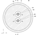
- FIG. 12 is a plan view showing the planar structure of the ground potential electrode section 4B.
- FIG. 13 is a plan view showing the planar structure of the bottom surface 21B of the metal casing 2B.
- An XYZ orthogonal coordinate system is shown in each of FIGS. 11 to 13.
- the DD cross section in FIG. 12 has the structure of the ground potential electrode portion 4B shown in FIG. 11, and the DD cross section in FIG. 13 has the structure of the metal casing 2B shown in FIG.
- the active gas generation device 53 of the third embodiment includes a metal casing 2B, an electrode structure, an AC power source 1, and shield dielectric films 8B1 and 8B2 as main components.
- the metal casing 2B is a casing that surrounds the internal casing space S2, and includes a casing bottom surface 21B and a casing side surface 22, the casing bottom surface 21B is a flat surface F2, and each is recessed in the depth direction from the flat surface F2. It has a bottom structure including two buffer spaces 9B1 and 9B2. The buffer spaces 9B1 and 9B2 are provided separated from each other across the flat surface F2 of the bottom surface 21B of the housing.
- the electrode structure is included as a main component of the high voltage application electrode section 3 and the ground potential electrode section 4B, and is arranged on the bottom surface 21B of the metal casing 2B so as to close the buffer spaces 9B1 and 9B2. has been done.
- the electrode structure includes a high voltage application electrode section 3 that is a first electrode component, and a ground potential electrode section 4B that is a second electrode component provided below the high voltage application electrode section 3. .
- the ground potential electrode part 4B which is the second electrode component, includes a second electrode dielectric film 40B, which is a second electrode dielectric film, and a second electrode dielectric film 40B, which is formed on the lower surface of the electrode dielectric film 40B. It includes an electrode conductive film 41B, which is a conductive film, and cover dielectric films 42B1 and 42B2.
- a cover dielectric film 42B1 which is a first cover dielectric film is provided on the lower surface of the electrode dielectric film 40B and the electrode conductive film 41B in the buffer space 9B1, and a cover dielectric film which is a second cover dielectric film is provided on the lower surface of the electrode dielectric film 40B and the electrode conductive film 41B in the buffer space 9B1.
- the body film 42B2 is provided on the lower surface of the electrode dielectric film 40B and the electrode conductive film 41B in the buffer space 9B2.
- the electrode dielectric film 40B and the cover dielectric films 42B1 and 42B2 are made of a dielectric, and the electrode conductive film 41B is made of a conductor such as metal.
- the electrode structure is arranged on the bottom surface of the metal casing 2B in such a manner that the electrode conductive film 41B and the flat surface F2 on the bottom surface 21B of the metal casing 2B are in contact with each other.
- the electrode dielectric film 40B has through holes 141 and 142, which are first and second dielectric through holes, and the through holes 141 and 142 are provided to penetrate the electrode dielectric film 40B.
- the through hole 141 overlaps with the buffer space 9B1 in plan view
- the through hole 142 overlaps with buffer space 9B2 in plan view.
- the cover dielectric film 42B1 which is the first cover dielectric film, has a through hole 151 in a region overlapping with the through hole 141 in plan view.
- a through hole 151 which is a first cover through hole, is provided to penetrate the cover dielectric film 42B1, and a through hole 152, which is a second cover through hole, is provided to penetrate the cover dielectric film 42B2.
- the through-hole 151 overlaps with the buffer space 9B1 in a plan view
- the through-hole 152 overlaps with the buffer space 9B2 in a plan view.
- the shield dielectric film 8B1 which is the first shield dielectric film, includes a region on the bottom surface of the buffer space 9B1 that overlaps with the through holes 141 and 151 in plan view, and includes the through holes 14, 15, and 151. Each opening 481 has a wider shape.
- the shield dielectric film 8B2, which is the second shield dielectric film includes a region on the bottom surface of the buffer space 9B2 that overlaps the through hole 142 and the through hole 152 in plan view, and The mouths 15 each have a wider shape.
- the bottom surface 21B of the metal casing 2B has two gas ejection ports 61 and 62 that are provided through the bottom surface of the buffer space 9B1 in the peripheral area of the shield dielectric film 8B1, which is the first shield dielectric film. are doing.
- the gas outlets 61 and 62 are both classified as first gas outlets provided at the bottom of the buffer space 9B1, which is the first buffer space.
- the bottom surface 21B of the metal casing 2B has two gas ejection ports 63 and 64 provided through the bottom surface of the buffer space 9B2 in the peripheral area of the shield dielectric film 8B2, which is the second shield dielectric film. are doing.
- the gas outlets 63 and 64 are both classified as second gas outlets provided at the bottom of the buffer space 9B2, which is the second buffer space.
- the gas ejection ports 61 and 62 both overlap with the cover dielectric film 42B1 in plan view, and do not overlap with the through holes 141 and 151 in plan view.
- the gas ejection ports 63 and 64 both overlap with the cover dielectric film 42B2 when viewed in plan, and do not overlap with the through holes 142 and 152 when viewed in plan.
- the combination of gas outlets 61 and 62 may be referred to as a "first gas outlet group”
- the combination of gas outlets 63 and 64 may be referred to as a "second gas outlet group”.
- An AC voltage is applied as an applied voltage from the AC power source 1 to the electrode conductive film 31, and the set potential, which is a reference potential, is applied to the second electrode conductive film through the housing bottom surface 21B of the metal housing 2B. It is applied to the film 41B.
- the space where the electrode dielectric film 30 and the electrode dielectric film 40B face each other is defined as a main dielectric space. Further, a space where the electrode dielectric film 30 and the shield dielectric film 8B1 face each other is defined as a first auxiliary dielectric space, and a space where the electrode dielectric film 30 and the shield dielectric film 8B2 face each other is defined as a first auxiliary dielectric space. 2 auxiliary dielectric space.
- a region where the electrode conductive films 31 and 41B overlap in plan view within the main dielectric space is defined as the main discharge space 50.
- a region including the through hole 141 and the through hole 151 within the first auxiliary dielectric space is defined as an auxiliary discharge space 581.
- This auxiliary discharge space 581 becomes the first auxiliary discharge space.
- a region including the through hole 142 and the through hole 152 within the second auxiliary dielectric space is defined as an auxiliary discharge space 582.
- This auxiliary discharge space 582 becomes a second auxiliary discharge space.
- Auxiliary discharge spaces 581 and 582, which are first and second auxiliary discharge spaces, are separated from each other.
- the auxiliary discharge space 581 further includes a part of the buffer space 9B1 above the shield dielectric film 8B1, and within the buffer space 9B1, the paths from the auxiliary discharge space 581 to each of the gas ejection ports 61 and 62 are first active. Defined as a gas distribution route. Therefore, the active gas G2 generated within the discharge space 5B is ejected from the gas ejection ports 61 and 62 toward the processing space 10 via the first active gas distribution path within the buffer space 9B1. As described above, the gas outlets 61 and 62 form the first gas outlet group.
- the auxiliary discharge space 582 further includes a part of the buffer space 9B2 above the shield dielectric film 8B2, and within the buffer space 9B2, the paths from the auxiliary discharge space 582 to each of the gas jet ports 63 and 64 are arranged as follows. It is defined as the active gas distribution route No. 2. Therefore, the active gas G2 generated within the discharge space 5B is ejected from the gas ejection ports 63 and 64 toward the processing space 10 via the second active gas distribution path within the buffer space 9B2. As described above, the gas outlets 63 and 64 form the first gas outlet group.
- the discharge space 5B in the active gas generation device 53 of the third embodiment includes the main discharge space 50, the auxiliary discharge space 581, and the auxiliary discharge space 582, and the first and second active gas distribution paths are completely separated from each other.
- the electrode dielectric film 40B and the electrode conductive film 41B each have a circular shape in plan view.
- the electrode dielectric film 40B has through holes 141 and 142 that are circular first and second dielectric through holes when viewed from above
- the electrode conductive film 41B has a circular shape when viewed from above. It has openings 481 and 482 that serve as first and second conductive film openings.
- the through-hole 141 and the opening 481 each overlap the buffer space 9B1 in plan view, and the opening 481 includes the through-hole 141 and has a wider shape than the through-hole 141 in plan view.
- the through-hole 142 and the opening 482 each overlap the buffer space 9B2 in plan view, and the opening 482 includes the through-hole 142 and has a wider shape than the through-hole 142 in plan view.
- the through holes 141 and 142 are arranged along the Y direction, and the through holes 151 and 152 are arranged surrounding the through holes 141 and 142 along the Y direction.
- the electrode conductive film 41B is provided on the lower surface of the electrode dielectric film 40B in such a manner that the center positions of the electrode dielectric film 40B and the electrode conductive film 41B are aligned.
- the diameter of the electrode conductive film 41B is set to be approximately the same as the diameter of the electrode dielectric film 40B, but since the openings 481 and 482 are wider than the through holes 141 and 142, the diameter of the electrode conductive film 41B is The formation area is smaller than the formation area of the electrode dielectric film 40B. Openings 481 and 482 become first and second conductor openings.
- the electrode boundary line 41L1 which is the circumferential outer circumference of the opening 481 that is the first conductive film opening, is the end of the electrode conductive film 41B on the through hole 141 side, and is the area inside the electrode boundary line 41L1.
- the electrode conductive film 41B is not formed on the electrode conductive film 41B.
- the electrode boundary line 41L2, which is the circumferential outer circumferential line of the opening 482, which is the second conductive film opening is the end of the electrode conductive film 41B on the through hole 142 side, and is closer to the electrode boundary line 41L2.
- the electrode conductive film 41B is not formed in the inner region.
- the electrode boundary lines 41L1 and 41L2 become the first and second electrode boundary lines.
- the cover dielectric film 42B1 has a circular shape extending from the lower surface of the electrode dielectric film 40B to the lower surface of the electrode conductive film 41B including the electrode boundary line 41L1, which is the first electrode boundary line. established in Therefore, the cover dielectric film 42B1 covers the electrode boundary line 41L1 of the electrode conductive film 41B. Further, the cover dielectric film 42B1 has a through hole 151, which includes all of the circular through hole 141 in plan view and is provided in a circular shape wider than the through hole 141.
- the cover dielectric film 42B2 is provided in a circular shape from the lower surface of the electrode dielectric film 40B to the lower surface of the electrode conductive film 41B including the electrode boundary line 41L2, which is the second electrode boundary line. Therefore, the cover dielectric film 42B2 covers the electrode boundary line 41L2 of the electrode conductive film 41B. Further, the cover dielectric film 42B2 has a through hole 152, which includes all of the circular through hole 142 in plan view and is provided in a circular shape that is wider than the through hole 142.
- the metal casing 2B has a circular casing bottom surface 21B and a casing side surface 22 erected in the height direction from the peripheral area of the casing bottom surface 21B. , each has two buffer spaces 9B1 and 9B2 recessed in the depth direction from the flat surface F2. Buffer spaces 9B1 and 9B2 are provided on the bottom surface 21B of the casing, separated from each other.
- the buffer spaces 9B1 and 9B2 and the shield dielectric films 8B1 and 8B2 each have a circular shape in plan view.
- the shield dielectric film 8B1 is provided on the bottom surface of the buffer space 9B1 in such a manner that the center positions of the buffer space 9B1 and the shield dielectric film 8B1 are aligned with each other. Since the diameter of the shield dielectric film 8B1 is shorter than the diameter of the buffer space 9B1, the formation area of the shield dielectric film 8B1 is narrower than the formation area of the bottom surface of the buffer space 9B1, and the peripheral area of the shield dielectric film 8B1 is smaller than the formation area of the bottom surface of the buffer space 9B1. This is the area where the bottom surface is exposed.
- the shield dielectric film 8B2 is provided on the bottom surface of the buffer space 9B2 in such a manner that the center positions of the buffer space 9B2 and the shield dielectric film 8B2 are aligned. Since the diameter of the shield dielectric film 8B2 is shorter than the diameter of the buffer space 9B2, the formation area of the shield dielectric film 8B2 is narrower than the formation area of the bottom surface of the buffer space 9B2, and the peripheral area of the shield dielectric film 8B2 is smaller than the formation area of the bottom surface of the buffer space 9B2. This is the area where the bottom surface is exposed.
- gas outlets 61 and 62 are provided in the peripheral region of the shield dielectric film 8B1 in the buffer space 9B1.
- gas outlets 63 and 64 are provided in the peripheral region of the shield dielectric film 8B2 in the buffer space 9B2.
- the gas outlets 61 and 62 are provided to penetrate the bottom surface of the buffer space 9B1, and the gas outlets 63 and 64 are provided to penetrate the bottom surface of the buffer space 9B2.
- Each of the gas ejection ports 61 to 64 has a vertical structure that extends vertically along the Z direction without tilting downward in the horizontal direction.
- the gas outlets 61 and 62 are provided symmetrically along the X direction with the shield dielectric film 8B1 in between, and the gas outlets 63 and 64 are provided symmetrically along the X direction with the shield dielectric film 8B2 in between. It will be done.
- Each of the gas outlets 61 to 64 functions as an orifice.
- the active gas generation device 53 of the third embodiment has the through holes 141 and 142 as the first and second dielectric through holes, and the through hole 151 as the first and second cover through holes. and 152, and has openings 481 and 482 as first and second conductive film openings.
- the active gas generation device 53 of the third embodiment has shield dielectric films 8B1 and 8B2 as the first and second shield dielectric films, and the gas jet ports 61 and 62 are included in the first gas jet port group.
- the gas ejection ports 63 and 64 are classified into the second gas ejection port group.
- the active gas generation device 53 of the third embodiment has buffer spaces 9B1 and 9B2 as the first and second buffer spaces, and cover dielectric films 42B1 and 42B2 as the first and second cover dielectric films. 42B2, and has shield dielectric films 8B1 and 8B2 as the first and second shield dielectric films.
- the electrode conductive film 41B of the active gas generation device 53 of Embodiment 3 has electrode boundary lines 41L1 and 41L2 as the first and second electrode boundary lines.
- the raw material gas G1 is supplied from the outside of the metal casing 2B into the interior space S2 of the casing through a supply port (not shown), as indicated by the broken line arrow in FIG. It is supplied to the discharge space 5B.
- the raw material gas G1 When the raw material gas G1 is supplied to the discharge space 5B where dielectric barrier discharge is occurring, the raw material gas G1 is activated and becomes an active gas G2, which passes through the through holes 141 and 151 and is introduced into the buffer space 9B1. and is introduced into the buffer space 9B2 through the through hole 142 and the through hole 152.
- the active gas G2 that has entered the buffer space 9B1 passes through gas outlets 61 and 62 that function as orifices provided at the bottom of the buffer space 9B1, and is supplied to the subsequent processing space 10.
- the active gas G2 that has entered the buffer space 9B2 passes through gas outlets 63 and 64 that function as orifices provided at the bottom of the buffer space 9B2, and is supplied to the subsequent processing space 10.
- discharge space 5B that generates the active gas G2 includes a main discharge space 50 and auxiliary discharge spaces 581 and 582.
- the shield dielectric film 8B1 is provided so that the bottom surface of the buffer space 9B1 in the metal case 2B and the auxiliary discharge space 581 are not in contact with each other, and the shield dielectric film 8B2 is provided so that the bottom surface of the buffer space 9B1 in the metal case 2B does not have a contact relationship with the buffer space 9B2 in the metal case 2B.
- the bottom surface of the auxiliary discharge space 582 is provided so as not to be in contact with the auxiliary discharge space 582.
- the bottom surfaces of the buffer spaces 9B1 and 9B2 are in contact with the auxiliary discharge spaces 581 and 582 with respect to the bottom surface 21B of the metal case 2B. This structure prevents metal ions from being mixed into the active gas G2.
- the active gas generation device 53 is configured to provide a cover dielectric film 42B1 covering the electrode boundary line 41L1 and a cover dielectric film 42B2 covering the electrode boundary line 41L2.
- 41L1 and 41L2 can be prevented from contacting the auxiliary discharge spaces 581 and 582.
- the active gas generation device 53 of Embodiment 3 adopts the electrode structure for dielectric barrier discharge as described above, so that in addition to the main discharge space 50, auxiliary discharge spaces 581 and 582 are formed, so that the discharge space is The volume of the discharge space 5B is expanded to extend the area of the discharge space 5B to a region relatively close to the gas jet ports 61 to 64 that function as orifices.
- the inactive state time until the active gas G2 generated in the discharge space 5B passes through the buffer spaces 9B1 and 9B2 outside the auxiliary discharge spaces 581 and 582 and is transferred to the gas jet ports 61 to 64 is shortened. can do. This is because the space volume of the first active gas flow path from the auxiliary discharge space 581 to the gas nozzles 61 and 62 is reduced, and the second active gas flow path from the auxiliary discharge space 582 to the gas nozzles 63 and 64 is reduced. This is because the spatial volume of the route can be reduced.
- the inactive state time is shortened, the possibility of gas collision deactivation due to collision between the source gas G1 and active gas G2 or collision/reaction between the active gases G2 can be suppressed.
- the active gas generating device 53 does not have a region in which each of the first and second active gas distribution paths is intentionally narrowed.
- the structure does not allow easy contact between the members constituting the generation device 53 and the first and second active gas flow paths. Therefore, in the active gas generation device 53 of the third embodiment, the possibility of surface deactivation can be suppressed to a low level.
- the active gas generation device 53 of Embodiment 3 includes auxiliary discharge spaces 581 and 582, which serve as first and second auxiliary discharge spaces, as part of the discharge space 5B.
- the auxiliary discharge space 581 includes the through hole 141 which is the first dielectric through hole, the through hole 151 which is the first cover through hole, and a part of the buffer space 9B1 which is the first buffer space.
- the auxiliary discharge space 582 includes the through hole 142 that is the second dielectric through hole, the through hole 152 that is the second cover through hole, and a part of the buffer space 9B2 that is the second buffer space.
- the cover dielectric film 42B1 of the ground potential electrode section 4B in the active gas generation device 53 of the third embodiment covers the electrode boundary line 41L1 in the buffer space 9B1, and also connects the gas jet ports 61 and 62 in plan view. Overlapping.
- the cover dielectric film 42B2 covers the electrode boundary line 41L2 in the buffer space 9B2, and overlaps with the gas jet ports 63 and 64 in plan view.
- the active gas generation device 53 of the third embodiment reliably avoids the surface deactivation phenomenon in which the active gas G2 in the buffer space 9B1 collides with the electrode conductive film 41B and the active gas G2 disappears. Can be done. In particular, the surface deactivation phenomenon of the active gas G2 above the gas jet ports 61 and 62 within the buffer space 9B1 can be reliably avoided.
- the surface deactivation phenomenon in which the active gas G2 in the buffer space 9B2 collides with the electrode conductive film 41B and the active gas G2 disappears can be reliably avoided.
- the surface deactivation phenomenon of the active gas G2 above the gas jet ports 63 and 64 within the buffer space 9B2 can be reliably avoided.
- the active gas generation device 53 of the third embodiment can supply highly concentrated active gas G2 from the gas jet ports 61 to 64 to the subsequent processing space 10. It is possible to exhibit the high concentration gas supply effect that can be achieved.
- the electrode structure in the active gas generation device 53 of the third embodiment does not have any conductive films other than the electrode conductive films 31 and 41B, the structure can be simplified as in the first embodiment. Can be done.
- the active gas G2 generated in the discharge space 5B is ejected from the gas ejection ports 61 and 62 via the above-mentioned first active gas distribution path, Further, the gas is ejected from the gas ejection ports 63 and 64 via the second active gas distribution path described above.
- the auxiliary discharge spaces 581 and 582 are provided separately from each other, the gas outlets 61 and 62 are classified into a first gas outlet group, and the gas outlets 63 and 64 are classified into a second gas outlet group. .
- the active gas generation device 53 of the third embodiment can operate the first gas outlet group (61, 62) and the second gas outlet group (63, 64) without reducing the concentration of the active gas G2. ) Since the active gas G2 can be ejected from each, the uniformity of the concentration of the supplied active gas can be improved.
- the gas jet ports 61 and 62 which are the first gas jet port group, are provided to penetrate the bottom surface of the buffer space 9B1, which is the first buffer space, and Gas jet ports 63 and 64, which are a group of gas jet ports, are provided to penetrate the bottom surface of the buffer space 9B2, which is a second buffer space.
- the buffer spaces 9B1 and 9B2 are provided separately from each other on the bottom surface 21B of the housing.
- the first active gas distribution path from the auxiliary discharge space 581 to the gas nozzles 61 and 62, and the second active gas distribution path from the auxiliary discharge space 582 to the gas nozzles 63 and 64, respectively, are completely closed. Can be separated.
- the active gas generation device 53 of Embodiment 3 ejects active gas G2 independent from each other from each of the first gas ejection port group (61, 62) and the second gas ejection port group (63, 64). be able to.
- the active gas generation device 53 of the third embodiment can supply the active gas G2 to the subsequent processing space 10 at a stable supply amount, similar to the active gas generation device 51 of the first embodiment.
- FIG. 14 is an explanatory diagram schematically showing a cross-sectional structure of an active gas generation device 54 according to Embodiment 4 of the present disclosure.
- FIG. 15 is a plan view showing the planar structure of the ground potential electrode section 4C.
- FIG. 16 is a plan view showing the planar structure of the bottom surface 22C of the metal casing 2C.
- An XYZ orthogonal coordinate system is shown in each of FIGS. 14 to 16.
- the EE cross section in FIG. 15 has the structure of the ground potential electrode portion 4C shown in FIG. 14, and the EE cross section in FIG. 16 has the structure of the metal casing 2C shown in FIG.
- the active gas generation device 54 of the fourth embodiment includes a metal casing 2C, an electrode structure, an AC power source 1, and a shield dielectric film 8C as main components.
- the metal housing 2C is a housing that surrounds the internal housing space S2, and includes a housing bottom surface 21C and a housing side surface 22.
- the housing bottom surface 21C includes a flat surface F2 and a buffer space 9C in the depth direction from the flat surface F2. It has a bottom structure that includes.
- the buffer space 9C becomes a common buffer space with a single structure.
- the electrode structure includes a high voltage application electrode section 3 and a ground potential electrode section 4C as main components, and is arranged on the bottom surface 21C of the metal casing 2C so as to close the buffer space 9C. There is.
- the electrode structure includes a high voltage application electrode section 3 that is a first electrode component and a ground potential electrode section 4C that is a second electrode component provided below the high voltage application electrode section 3. .
- the ground potential electrode part 4C which is the second electrode component, includes a second electrode dielectric film 40B, which is a second electrode dielectric film, and a second electrode dielectric film 40B, which is formed on the lower surface of the electrode dielectric film 40B. It includes an electrode conductive film 41C, which is a conductive film, and a cover dielectric film 42C.
- the cover dielectric film 42C is provided on the lower surface of the electrode dielectric film 40B and the electrode conductive film 41C in the buffer space 9C.
- the electrode conductive film 41C and the cover dielectric film 42C are made of a dielectric, and the electrode conductive film 41C is made of a conductor such as metal.
- the electrode structure is arranged on the bottom surface 21C of the metal casing 2C in such a manner that the conductive film 41C for the electrode of the electrode structure contacts the flat surface F2 on the bottom surface 21C of the metal casing 2C.
- the electrode dielectric film 40B which is the second electrode dielectric film, has first and second dielectric through holes penetrating the electrode dielectric film 40B in an area overlapping with the buffer space 9C in plan view. It has certain through holes 141 and 142.
- the cover dielectric film 42C which is a common cover dielectric film with a single structure, has a through hole 151, which is a first cover through hole, in a region overlapping with the through hole 141 when viewed from above, and has a through hole 151 that is a first cover through hole when viewed from above.
- a through hole 152 which is a second cover through hole, is provided in an area overlapping with 142. The through holes 151 and 152 are provided to penetrate the cover dielectric film 42C.
- the shield dielectric film 8C which is a common shield dielectric film with a single structure, overlaps the through holes 141 and 151 in a plan view on the bottom surface of the buffer space 9C, and overlaps the through holes 141 and 151 in a plan view. and is provided in an area overlapping with the through hole 152.
- the bottom surface 21C of the metal casing 2C has gas outlets 61 to 64 in the peripheral area of the shield dielectric film 8C, which is a common shield dielectric film.
- the gas outlets 61 and 62 are classified into a first gas outlet group, and the gas outlets 63 and 64 are classified into a second gas outlet group.
- Each of the gas jet ports 61 to 64 is provided to penetrate the bottom surface of the buffer space 9C.
- gas ejection ports 61 and 62 classified as the first gas ejection ports both overlap with the cover dielectric film 42C in plan view, and do not overlap with the through holes 141 and 151 in plan view.
- gas outlets 63 and 64 classified as second gas outlets overlap with cover dielectric film 42C in plan view, and do not overlap with through holes 142 and 152 in plan view. .
- An AC voltage is applied as an applied voltage from the AC power supply 1 to the electrode conductive film 31, which is the first electrode conductive film, and the set potential, which is the reference potential, is applied to the second electrode conductive film 31, which is the first electrode conductive film, through the housing bottom surface 21C of the metal housing 2C. It is applied to the conductive film for electrode 41C which is the conductive film for electrode.
- the space where the electrode dielectric film 30 and the electrode dielectric film 40B face each other is defined as the main dielectric space. Further, two spaces where the electrode dielectric film 30 and the shield dielectric film 8C face each other are defined as first and second auxiliary dielectric spaces.
- a region where the electrode conductive films 31 and 41 overlap in plan view within the main dielectric space is defined as the main discharge space 50.
- a region including the through hole 141 and the through hole 151 within the first auxiliary dielectric space is defined as an auxiliary discharge space 581.
- the auxiliary discharge space 581 becomes the first auxiliary discharge space.
- a region including the through hole 142 and the through hole 152 within the second auxiliary dielectric space is defined as an auxiliary discharge space 582.
- the auxiliary discharge space 582 becomes the second auxiliary discharge space.
- the auxiliary discharge space 581 includes the through hole 141, the through hole 151, and a part of the buffer space 9C below the through hole 151.
- a path from the auxiliary discharge space 581 to each of the gas jet ports 61 and 62 in the buffer space 9C is defined as a first active gas distribution path.
- the active gas G2 generated in the discharge space 5C is ejected from the gas ejection ports 61 and 62 toward the processing space 10 via the first active gas distribution path in the auxiliary discharge space 581 and the buffer space 9C. be done.
- the gas outlets 61 and 62 form the first gas outlet group.
- the auxiliary discharge space 582 includes the through hole 142, the through hole 152, and a part of the buffer space 9C below the through hole 152. Paths from the auxiliary discharge space 582 to the gas jet ports 63 and 64 in the buffer space 9C are defined as second active gas distribution paths.
- the active gas G2 generated in the discharge space 5C is ejected from the gas ejection ports 63 and 64 toward the processing space 10 via the auxiliary discharge space 582 and the second active gas distribution path in the buffer space 9C. be done.
- the gas outlets 63 and 64 form the second gas outlet group.
- the auxiliary discharge spatial distance between the auxiliary discharge spaces 581 and 582, and the distance between the gas nozzle groups between the gas nozzles 61 and 62 and the gas nozzles 63 and 64 are determined by the first active gas flow within the buffer space 9C, respectively.
- the length is set to such an extent that no interference occurs between the active gas G2 flowing through the path and the active gas G2 flowing through the second active gas distribution path.
- the auxiliary discharge spaces 581 and 582 both include a part of the buffer space 9C, the auxiliary discharge spaces 581 and 582 are provided separately from each other.
- the first gas outlet group (61, 62) and the second gas outlet group (63, 64) are provided through the bottom of the same buffer space 9C, but the first and second gas outlet groups (61, 62) are provided through the bottom surface of the same buffer space 9C.
- the gas ejection port groups are provided separately from each other.
- the discharge space 5C in the active gas generation device 54 of the fourth embodiment includes the main discharge space 50, the auxiliary discharge space 581, and the auxiliary discharge space 582.
- the electrode dielectric film 40B and the electrode conductive film 41C each have a circular shape in plan view.
- the electrode dielectric film 40B has through holes 141 and 142 which are circular first and second dielectric through holes when viewed from above
- the electrode conductive film 41C has a circular shape when viewed from above. It has openings 481 and 482 that serve as first and second conductive film openings.
- the through holes 141 and 142 and the openings 481 and 482 each overlap with the buffer space 9C in plan view, and the opening 481 includes the through hole 141 in plan view, has a wider shape than the through hole 141, and has a shape that is wider than the through hole 141.
- the portion 482 includes the through hole 142 in plan view and has a shape wider than the through hole 142.
- the through holes 141 and 142 are arranged along the Y direction, and the through holes 151 and 152 are arranged so as to be surrounded by the through holes 141 and 142 along the Y direction.
- a conductive film 41C for an electrode is provided on the lower surface of the dielectric film 40B for an electrode in such a manner that the center positions of the dielectric film 40B for an electrode and the conductive film 41C for an electrode are aligned.
- the diameter of the electrode conductive film 41C is set to be approximately the same as the diameter of the electrode dielectric film 40B, but since the openings 481 and 482 are wider than the through holes 141 and 142, the diameter of the electrode conductive film 41B is The formation area is smaller than the formation area of the electrode dielectric film 40C. Openings 481 and 482 become first and second conductor openings.
- the electrode boundary line 41L1 which is the circumferential outer circumference of the opening 481 that is the first conductive film opening, is the end of the electrode conductive film 41B on the through hole 141 side, and is the area inside the electrode boundary line 41L1. 41C of conductive films for electrodes are not formed.
- the electrode conductive film 41C is not formed in the inner region.
- the electrode boundary lines 41L1 and 41L2 become the first and second electrode boundary lines.
- the cover dielectric film 42C has a vertically elongated shape with semicircular ends at both ends in the Y direction when viewed from above.
- the first partial region on the +Y direction side from the center of the cover dielectric film 42C is provided from the lower surface of the electrode dielectric film 40B to the lower surface of the electrode conductive film 41B including the electrode boundary line 41L1. Therefore, the cover dielectric film 42C covers the electrode boundary line 41L1 of the electrode conductive film 41B.
- a second partial region on the ⁇ Y direction side from the center of the cover dielectric film 42C is provided from the lower surface of the electrode dielectric film 40B to the lower surface of the electrode conductive film 41B including the electrode boundary line 41L2. It will be done. Therefore, the cover dielectric film 42C covers the electrode boundary line 41L2 of the electrode conductive film 41B.
- the first partial region of the cover dielectric film 42C has a through hole 151, and this through hole 151 includes all of the circular through hole 141 in plan view and is provided in a circular shape wider than the through hole 141. It will be done.
- the second partial region of the cover dielectric film 42C has a through hole 152, which includes the entire circular through hole 142 in plan view and has a circular shape wider than the through hole 142. provided.
- the metal casing 2C has a circular casing bottom surface 21C and a casing side surface 22 erected in the height direction from the peripheral area of the casing bottom surface 21C. , it has a buffer space 9C recessed in the depth direction from the flat surface F2.
- the buffer space 9C and the shield dielectric film 8C each have a vertically elongated shape with semicircular ends at both ends in the Y direction when viewed from above.
- a shield dielectric film 8C is provided on the bottom surface of the buffer space 9C in such a manner that the centers of the buffer space 9C and the shield dielectric film 8C are aligned.
- the area where the shield dielectric film 8C is formed is smaller than the area where the bottom surface of the buffer space 9C is formed.
- gas outlets 61 to 64 are provided in the peripheral area of the shield dielectric film 8C on the bottom surface of the buffer space 9C.
- the gas outlets 61 and 62 are provided symmetrically along the X direction with the shield dielectric film 8C in between, and the gas outlets 63 and 64 are provided symmetrically along the X direction with the shield dielectric film 8C in between. It will be done.
- the gas outlets 61 to 64 are classified into a first gas outlet group, and the gas outlets 63 and 64 are classified into a second gas outlet group.
- the distance between the gas jet ports 61 and 62 and the gas jet ports 63 and 64 is set longer than the distance between the gas jet ports 61 and 62 and the distance between the gas jet ports 63 and 64.
- the active gas generation device 54 of the fourth embodiment has the through holes 141 and 142 as the first and second dielectric through holes, and the through hole 151 as the first and second cover through holes. and 152, and has openings 481 and 482 as first and second conductive film openings.
- the gas outlets 61 and 62 are classified into the first gas outlet group, and the gas outlets 63 and 64 are classified into the second gas outlet group.
- the active gas generation device 54 of the fourth embodiment has a buffer space 9C as a common buffer space, a shield dielectric film 8C as a common cover dielectric film, and a shield dielectric film as a common shield dielectric film. It has a membrane 8C.
- the electrode conductive film 41C of the active gas generation device 54 of Embodiment 4 has electrode boundary lines 41L1 and 41L2 as the first and second electrode boundary lines.
- the raw material gas G1 is supplied from the outside of the metal casing 2C into the interior space S2 of the casing through a supply port (not shown), as indicated by the broken line arrow in FIG. It is supplied to the discharge space 5C.
- the raw material gas G1 When the raw material gas G1 is supplied to the discharge space 5C where dielectric barrier discharge is occurring, the raw material gas G1 is activated and becomes an active gas G2, which passes through the through holes 141 and 151 and is introduced into the buffer space 9C. and is introduced into the buffer space 9C through the through holes 142 and 152.
- the active gas G2 that has entered the buffer space 9C passes through gas outlets 61 to 64 that function as orifices provided at the bottom of the buffer space 9C, and is supplied to the subsequent processing space 10.
- discharge space 5C that generates the active gas G2 includes a main discharge space 50 and auxiliary discharge spaces 581 and 582.
- the shield dielectric film 8C is provided so that the bottom surface of the buffer space 9C in the metal casing 2C and the auxiliary discharge spaces 581 and 582 are not in contact with each other.
- the bottom surface of the buffer space 9C does not touch the auxiliary discharge spaces 581 and 582 with respect to the bottom surface 21C of the metal case 2C. This prevents metal ions from being mixed into the active gas G2.
- the electric field strength tends to increase at the electrode boundary lines 41L1 and 41L2, which are the outer peripheries of the openings 481 and 482 of the electrode conductive film 41C of the ground potential electrode section 4C, and in the vicinity thereof. Therefore, by providing the cover dielectric film 42C to cover the electrode boundary lines 41L1 and 41L2, it is possible to prevent the electrode boundary lines 41L1 and 41L2 of the electrode conductive film 41C from coming into contact with the auxiliary discharge spaces 581 and 582.
- the active gas generation device 54 of Embodiment 4 adopts the electrode structure for dielectric barrier discharge as described above, so that in addition to the main discharge space 50, auxiliary discharge spaces 581 and 582 are formed, so that the discharge space is The volume of the discharge space 5C is expanded to extend the area of the discharge space 5C to a region relatively close to the gas jet ports 61 to 64 that function as orifices.
- the active gas G2 generated in the discharge space 5C passes through the buffer space 9C outside the auxiliary discharge spaces 581 and 582,
- the inactive state time until being transferred to the jet ports 61 to 64 can be shortened.
- the inactive state time is shortened, the possibility of gas collision deactivation due to collision between the source gas G1 and active gas G2 or collision/reaction between the active gases G2 can be suppressed.
- the active gas generating device 54 does not have a region in which each of the first and second active gas distribution paths is intentionally narrowed, so that the active gas
- the structure does not allow easy contact between the members constituting the generation device 54 and the first and second active gas flow paths. Therefore, in the active gas generation device 54 of the fourth embodiment, the possibility of surface deactivation can be suppressed to a low level.
- the auxiliary discharge space 581 that is a part of the discharge space 5C has a through hole 141 that is a first dielectric through hole and a through hole 151 that is a first cover through hole. It also includes a part of the buffer space 9C which is a common buffer space. Similarly, the auxiliary discharge space 582 includes the through hole 142 which is the second dielectric through hole, the through hole 152 which is the second cover through hole, and a part of the buffer space 9C.
- cover dielectric film 42C of the ground potential electrode section 4C in the active gas generation device 54 of the fourth embodiment covers the electrode boundary lines 41L1 and 41L2 in the buffer space 9C, and also covers the gas jet ports 61 to 41L2 in the buffer space 9C. It overlaps with 64.
- the active gas generation device 54 of the fourth embodiment reliably avoids the surface deactivation phenomenon in which the active gas G2 in the buffer space 9C collides with the electrode conductive film 41C and the active gas G2 disappears. Can be done. In particular, the surface deactivation phenomenon of the active gas G2 above the gas jet ports 61 to 64 in the buffer space 9C can be reliably avoided.
- the active gas generation device 54 of the fourth embodiment like the active gas generation device 51 of the first embodiment, supplies highly concentrated active gas G2 from the gas jet ports 61 to 64 to the subsequent processing space 10. It is possible to exhibit the high concentration gas supply effect that can be achieved.
- the electrode structure in the active gas generation device 54 of the fourth embodiment does not have any conductive films other than the electrode conductive films 31 and 41B, it exhibits the effect of simplifying the structure as in the first embodiment. Can be done.
- the active gas G2 generated in the discharge space 5C is ejected from the gas ejection ports 61 and 62 via the above-described first active gas distribution path, In addition, the gas is ejected from the gas ejection ports 63 and 64 via the second active gas distribution path described above.
- the auxiliary discharge spaces 581 and 582 are provided separately from each other, the gas outlets 61 and 62 are classified into a first gas outlet group, and the gas outlets 63 and 64 are classified into a second gas outlet group. .
- the active gas generation device 54 of the fourth embodiment can improve the uniformity of the concentration of the supplied active gas, similar to the third embodiment.
- the active gas generation device 54 of the fourth embodiment includes a buffer space 9C that is a common buffer space with a single structure, a cover dielectric film 42C that is a common cover dielectric film with a single structure, and a common shield dielectric with a single structure. It includes a shield dielectric film 8C which is a film.
- the gas outlets 61 to 64 are provided to penetrate the bottom surface of the buffer space 9C, and the shield dielectric film 8C is provided on the bottom surface of the buffer space 9C.
- the buffer space 9C, the cover dielectric film 42C, and the shield dielectric film 8C have a single structure, compared to the active gas generation device 53 of the third embodiment. The number of parts can be reduced.
- the active gas generation device 54 of Embodiment 4 ejects the active gas G2 from the first gas ejection port group (61, 62) and the second gas ejection port group (63, 64) which are separated from each other. , it is possible to improve the uniformity of the concentration of the active gas G2.
- the quantity ratio N is increased from “2" to "4" compared to the first to third embodiments, so that the active gas generation device 54 is more effective.
- the active gas G2 can be supplied to the subsequent processing space 10 at a stable supply amount.
- the embodiments of the present disclosure can be freely combined, and the embodiments can be modified or omitted as appropriate.
- the gas ejection ports 61 to 64 of the active gas generation device 53 of the third embodiment and the active gas generation device 54 of the fourth embodiment may be changed from the vertical structure to the gas ejection ports of the active gas generation device 52 of the second embodiment.
- the structure may be changed to a diagonal structure like 71 and 72.
- the third embodiment shows a structure in which two dielectric through holes, an auxiliary discharge space, a buffer space, a cover dielectric film, a shield dielectric film, etc. are provided
- the active gas generation device 53 of the third embodiment is expanded.
- three or more dielectric through holes, auxiliary discharge spaces, buffer spaces, cover dielectric films, shield dielectric films, etc. may be provided.
- the active gas generation device 53 of Embodiment 4 can be expanded to include dielectric through holes, auxiliary discharge spaces, etc. "3" or more may be provided.
Landscapes
- Physics & Mathematics (AREA)
- Engineering & Computer Science (AREA)
- Plasma & Fusion (AREA)
- Chemical & Material Sciences (AREA)
- Analytical Chemistry (AREA)
- Spectroscopy & Molecular Physics (AREA)
- Plasma Technology (AREA)
Priority Applications (7)
| Application Number | Priority Date | Filing Date | Title |
|---|---|---|---|
| PCT/JP2022/020652 WO2023223454A1 (ja) | 2022-05-18 | 2022-05-18 | 活性ガス生成装置 |
| JP2022564749A JP7297399B1 (ja) | 2022-05-18 | 2022-05-18 | 活性ガス生成装置 |
| US18/570,654 US12424418B2 (en) | 2022-05-18 | 2022-05-18 | Active gas generation apparatus |
| KR1020237040733A KR102805775B1 (ko) | 2022-05-18 | 2022-05-18 | 활성 가스 생성 장치 |
| CN202280037972.0A CN117426143A (zh) | 2022-05-18 | 2022-05-18 | 活性气体生成装置 |
| EP22942659.8A EP4340548B1 (en) | 2022-05-18 | 2022-05-18 | Active-gas-generating apparatus |
| TW112105618A TWI841245B (zh) | 2022-05-18 | 2023-02-16 | 活性氣體生成裝置 |
Applications Claiming Priority (1)
| Application Number | Priority Date | Filing Date | Title |
|---|---|---|---|
| PCT/JP2022/020652 WO2023223454A1 (ja) | 2022-05-18 | 2022-05-18 | 活性ガス生成装置 |
Publications (1)
| Publication Number | Publication Date |
|---|---|
| WO2023223454A1 true WO2023223454A1 (ja) | 2023-11-23 |
Family
ID=86900451
Family Applications (1)
| Application Number | Title | Priority Date | Filing Date |
|---|---|---|---|
| PCT/JP2022/020652 Ceased WO2023223454A1 (ja) | 2022-05-18 | 2022-05-18 | 活性ガス生成装置 |
Country Status (7)
| Country | Link |
|---|---|
| US (1) | US12424418B2 (https=) |
| EP (1) | EP4340548B1 (https=) |
| JP (1) | JP7297399B1 (https=) |
| KR (1) | KR102805775B1 (https=) |
| CN (1) | CN117426143A (https=) |
| TW (1) | TWI841245B (https=) |
| WO (1) | WO2023223454A1 (https=) |
Cited By (1)
| Publication number | Priority date | Publication date | Assignee | Title |
|---|---|---|---|---|
| JP7493905B1 (ja) * | 2023-05-01 | 2024-06-03 | 株式会社Tmeic | 活性ガス生成装置 |
Families Citing this family (3)
| Publication number | Priority date | Publication date | Assignee | Title |
|---|---|---|---|---|
| CN114916255B (zh) * | 2020-12-07 | 2025-09-23 | 株式会社Tmeic | 活性气体生成装置 |
| EP4340548B1 (en) * | 2022-05-18 | 2025-10-15 | TMEIC Corporation | Active-gas-generating apparatus |
| WO2024084640A1 (ja) * | 2022-10-20 | 2024-04-25 | 東芝三菱電機産業システム株式会社 | 活性ガス生成装置 |
Citations (5)
| Publication number | Priority date | Publication date | Assignee | Title |
|---|---|---|---|---|
| JP2016085935A (ja) * | 2014-10-29 | 2016-05-19 | 東芝三菱電機産業システム株式会社 | 窒素ラジカル生成システム |
| WO2018104988A1 (ja) * | 2016-12-05 | 2018-06-14 | 東芝三菱電機産業システム株式会社 | 活性ガス生成装置 |
| WO2019229873A1 (ja) * | 2018-05-30 | 2019-12-05 | 東芝三菱電機産業システム株式会社 | 活性ガス生成装置 |
| JP6873588B1 (ja) | 2019-11-12 | 2021-05-19 | 東芝三菱電機産業システム株式会社 | 活性ガス生成装置 |
| WO2021106100A1 (ja) * | 2019-11-27 | 2021-06-03 | 東芝三菱電機産業システム株式会社 | 活性ガス生成装置 |
Family Cites Families (24)
| Publication number | Priority date | Publication date | Assignee | Title |
|---|---|---|---|---|
| US5605637A (en) * | 1994-12-15 | 1997-02-25 | Applied Materials Inc. | Adjustable dc bias control in a plasma reactor |
| US5982100A (en) * | 1997-07-28 | 1999-11-09 | Pars, Inc. | Inductively coupled plasma reactor |
| US9490106B2 (en) * | 2011-04-28 | 2016-11-08 | Lam Research Corporation | Internal Faraday shield having distributed chevron patterns and correlated positioning relative to external inner and outer TCP coil |
| US10573496B2 (en) * | 2014-12-09 | 2020-02-25 | Applied Materials, Inc. | Direct outlet toroidal plasma source |
| US20160225652A1 (en) * | 2015-02-03 | 2016-08-04 | Applied Materials, Inc. | Low temperature chuck for plasma processing systems |
| CN104812154A (zh) * | 2015-04-22 | 2015-07-29 | 西安交通大学 | 一种三电极介质阻挡放电等离子体发生装置 |
| US10504754B2 (en) * | 2016-05-19 | 2019-12-10 | Applied Materials, Inc. | Systems and methods for improved semiconductor etching and component protection |
| US10522371B2 (en) * | 2016-05-19 | 2019-12-31 | Applied Materials, Inc. | Systems and methods for improved semiconductor etching and component protection |
| WO2019049230A1 (ja) * | 2017-09-06 | 2019-03-14 | 東芝三菱電機産業システム株式会社 | 活性ガス生成装置 |
| US10854426B2 (en) * | 2018-01-08 | 2020-12-01 | Applied Materials, Inc. | Metal recess for semiconductor structures |
| WO2019138456A1 (ja) * | 2018-01-10 | 2019-07-18 | 東芝三菱電機産業システム株式会社 | 活性ガス生成装置 |
| US10593560B2 (en) * | 2018-03-01 | 2020-03-17 | Applied Materials, Inc. | Magnetic induction plasma source for semiconductor processes and equipment |
| JP2019160714A (ja) * | 2018-03-16 | 2019-09-19 | 株式会社日立ハイテクノロジーズ | プラズマ処理装置 |
| KR102510329B1 (ko) * | 2018-06-25 | 2023-03-17 | 도시바 미쓰비시덴키 산교시스템 가부시키가이샤 | 활성 가스 생성 장치 및 성막 처리 장치 |
| US10892198B2 (en) * | 2018-09-14 | 2021-01-12 | Applied Materials, Inc. | Systems and methods for improved performance in semiconductor processing |
| JP6844937B2 (ja) * | 2019-02-13 | 2021-03-17 | 東芝三菱電機産業システム株式会社 | 活性ガス生成装置 |
| US12295089B2 (en) * | 2020-02-27 | 2025-05-06 | Tmeic Corporation | Active gas generation apparatus |
| JP7351245B2 (ja) * | 2020-03-13 | 2023-09-27 | ウシオ電機株式会社 | 誘電体バリア式プラズマ発生装置、及び、誘電体バリア式プラズマ発生装置のプラズマ放電開始方法 |
| US12512304B2 (en) * | 2020-07-23 | 2025-12-30 | Applied Materials, Inc. | Plasma source for semiconductor processing |
| JP2022049503A (ja) * | 2020-09-16 | 2022-03-29 | 株式会社東芝 | 誘電体バリア放電電極及び誘電体バリア放電装置 |
| KR102606837B1 (ko) * | 2021-11-02 | 2023-11-29 | 피에스케이 주식회사 | 상부 전극 유닛, 그리고 이를 포함하는 기판 처리 장치 |
| US12080516B2 (en) * | 2021-11-23 | 2024-09-03 | Applied Materials, Inc. | High density plasma enhanced process chamber |
| EP4340548B1 (en) * | 2022-05-18 | 2025-10-15 | TMEIC Corporation | Active-gas-generating apparatus |
| WO2024084640A1 (ja) * | 2022-10-20 | 2024-04-25 | 東芝三菱電機産業システム株式会社 | 活性ガス生成装置 |
-
2022
- 2022-05-18 EP EP22942659.8A patent/EP4340548B1/en active Active
- 2022-05-18 KR KR1020237040733A patent/KR102805775B1/ko active Active
- 2022-05-18 US US18/570,654 patent/US12424418B2/en active Active
- 2022-05-18 WO PCT/JP2022/020652 patent/WO2023223454A1/ja not_active Ceased
- 2022-05-18 JP JP2022564749A patent/JP7297399B1/ja active Active
- 2022-05-18 CN CN202280037972.0A patent/CN117426143A/zh active Pending
-
2023
- 2023-02-16 TW TW112105618A patent/TWI841245B/zh active
Patent Citations (6)
| Publication number | Priority date | Publication date | Assignee | Title |
|---|---|---|---|---|
| JP2016085935A (ja) * | 2014-10-29 | 2016-05-19 | 東芝三菱電機産業システム株式会社 | 窒素ラジカル生成システム |
| WO2018104988A1 (ja) * | 2016-12-05 | 2018-06-14 | 東芝三菱電機産業システム株式会社 | 活性ガス生成装置 |
| WO2019229873A1 (ja) * | 2018-05-30 | 2019-12-05 | 東芝三菱電機産業システム株式会社 | 活性ガス生成装置 |
| JP6873588B1 (ja) | 2019-11-12 | 2021-05-19 | 東芝三菱電機産業システム株式会社 | 活性ガス生成装置 |
| WO2021095120A1 (ja) * | 2019-11-12 | 2021-05-20 | 東芝三菱電機産業システム株式会社 | 活性ガス生成装置 |
| WO2021106100A1 (ja) * | 2019-11-27 | 2021-06-03 | 東芝三菱電機産業システム株式会社 | 活性ガス生成装置 |
Non-Patent Citations (1)
| Title |
|---|
| See also references of EP4340548A4 |
Cited By (1)
| Publication number | Priority date | Publication date | Assignee | Title |
|---|---|---|---|---|
| JP7493905B1 (ja) * | 2023-05-01 | 2024-06-03 | 株式会社Tmeic | 活性ガス生成装置 |
Also Published As
| Publication number | Publication date |
|---|---|
| JPWO2023223454A1 (https=) | 2023-11-23 |
| CN117426143A (zh) | 2024-01-19 |
| US20240297024A1 (en) | 2024-09-05 |
| TWI841245B (zh) | 2024-05-01 |
| JP7297399B1 (ja) | 2023-06-26 |
| EP4340548A1 (en) | 2024-03-20 |
| TW202405233A (zh) | 2024-02-01 |
| EP4340548B1 (en) | 2025-10-15 |
| US12424418B2 (en) | 2025-09-23 |
| KR20240004639A (ko) | 2024-01-11 |
| KR102805775B1 (ko) | 2025-05-14 |
| EP4340548A4 (en) | 2025-04-16 |
Similar Documents
| Publication | Publication Date | Title |
|---|---|---|
| WO2023223454A1 (ja) | 活性ガス生成装置 | |
| KR101245433B1 (ko) | 이온 발생 장치 및 전기 기기 | |
| KR102545951B1 (ko) | 활성 가스 생성 장치 | |
| JP6851706B2 (ja) | 活性ガス生成装置 | |
| KR20210087531A (ko) | 활성 가스 생성 장치 | |
| US10971338B2 (en) | Active gas generating apparatus | |
| KR880009539A (ko) | 이온 발생 장치 | |
| JP6678232B2 (ja) | プラズマ発生装置 | |
| US7706121B2 (en) | Ion generator | |
| JP2010539373A (ja) | 高電圧絶縁装置および、当該高電圧絶縁装置を備えたイオン加速装置 | |
| EP3609302B1 (en) | Plasma-generating device | |
| US7532450B2 (en) | Surge suppressor | |
| US4378511A (en) | Tube socket assembly with corona disrupter | |
| JP2014121424A (ja) | 放電ユニットおよびこれを用いた空気清浄装置 | |
| JP2004139978A (ja) | 画像表示装置及び情報表示装置 | |
| JP7493905B1 (ja) | 活性ガス生成装置 | |
| KR20250090329A (ko) | 활성 가스 생성 장치 | |
| JP4629394B2 (ja) | 蒸着源と蒸着装置 | |
| CN120111760A (zh) | 等离子体放电装置及其控制方法 | |
| CN110506453B (zh) | 等离子体发生装置 | |
| JP5382776B2 (ja) | パルス発生装置 | |
| JP2002220209A (ja) | オゾン発生装置 | |
| JP2010238487A (ja) | 負イオン源 |
Legal Events
| Date | Code | Title | Description |
|---|---|---|---|
| ENP | Entry into the national phase |
Ref document number: 2022564749 Country of ref document: JP Kind code of ref document: A |
|
| ENP | Entry into the national phase |
Ref document number: 20237040733 Country of ref document: KR Kind code of ref document: A |
|
| WWE | Wipo information: entry into national phase |
Ref document number: 202280037972.0 Country of ref document: CN |
|
| WWE | Wipo information: entry into national phase |
Ref document number: 2022942659 Country of ref document: EP |
|
| ENP | Entry into the national phase |
Ref document number: 2022942659 Country of ref document: EP Effective date: 20231215 |
|
| 121 | Ep: the epo has been informed by wipo that ep was designated in this application |
Ref document number: 22942659 Country of ref document: EP Kind code of ref document: A1 |
|
| NENP | Non-entry into the national phase |
Ref country code: DE |
|
| WWG | Wipo information: grant in national office |
Ref document number: 18570654 Country of ref document: US |
|
| WWG | Wipo information: grant in national office |
Ref document number: 2022942659 Country of ref document: EP |